

What is Time-Domain Reflectometry (TDR)?
Time-Domain Reflectometry (TDR) is a valuable technique for diverse applications such as evaluating power distribution networks and ensuring signal path integrity.
Time-Domain Reflectometry (TDR) has evolved from being a simple fault-locating tool to an indispensable technique for modern electrical engineers. Along with fault detection, today’s TDR systems offer sophisticated analysis capabilities that provide valuable insights to help optimize power and signal integrity across various applications -- from evaluating power rails on PCBs to ensuring cable integrity.
As a time-domain technique, TDR employs oscilloscopes for precise signal measurement and analysis. Sampling oscilloscopes, known for their excellent time and voltage resolution, are particularly suited for repetitive waveforms. However, real-time oscilloscopes, which capture and analyze single-shot events, are more common on engineering benches. Despite the different sampling techniques, the underlying theory of TDR remains the same. A typical TDR measurement setup includes an oscilloscope, a pulse/step generator with fast edges, high-quality cables, and power splitters. Dedicated TDR step generators are also available, integrating a step generator and power splitter to streamline the measurement process. This primer focuses on TDR measurement techniques with the use of general-purpose, real-time oscilloscopes in combination with a dedicated TDR step generator.
This primer:
- Describes applications for time domain reflectometry (TDR)
- Explains the theory behind TDR
- Explains how TDR works in practice
- Describes types of TDR measurements
- Explains how to set up TDR measurements with a real-time oscilloscope
- Gives TDR measurement examples
Although TDR is often performed with sampling oscilloscopes, it can also be employed with real-time oscilloscopes. The theory behind TDR is the same, regardless of the acquisition technology used in the scope. High bandwidth is desirable since it translates into the ability to discern impedance discontinuities. In this primer, a 10 GHz 6 Series B MSO is used with a Picotest PerfectPulse® step source. The oscilloscope is equipped with Option 6-TDR, which automates setup and measurements. Similar options are available for the 5 Series MSO (Option 5-TDR) and 4 Series MSO (Option 4-TDR) at lower bandwidth points.
Applications of TDR
TDR is invaluable for ensuring the integrity of signal paths and power distribution networks. Maintaining uniform impedance minimizes voltage fluctuations and noise on signal paths and power rails. By analyzing impedance waveforms, engineers can identify discontinuities and mismatches. Opens and shorts may be considered special cases of impedances. As such, TDR is an ideal tool for identifying and locating opens and shorts.
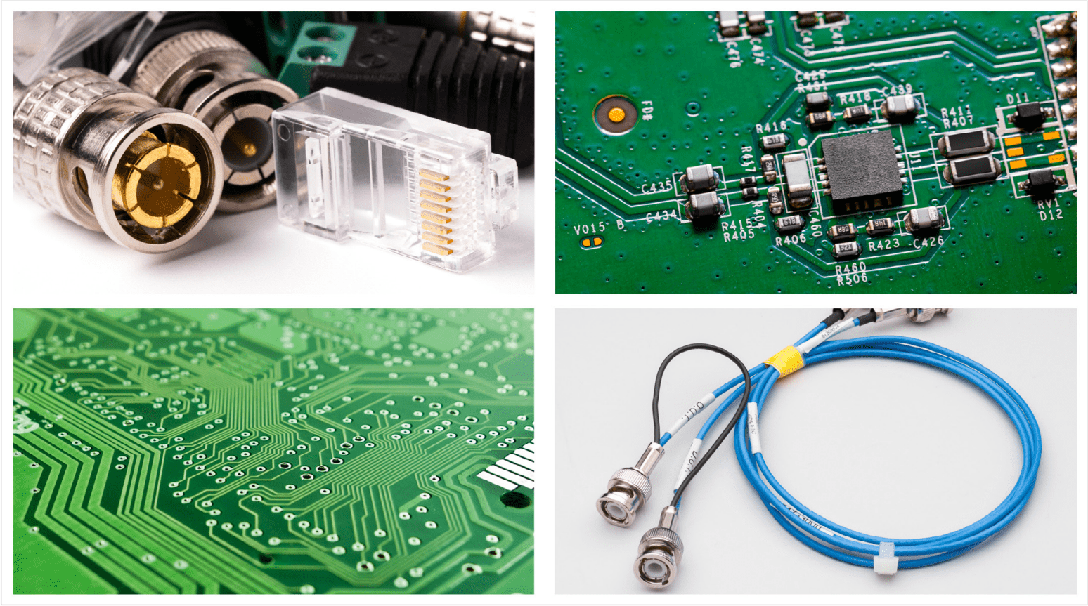
TDR can be applied to any area that behaves like a transmission line. Some examples are shown in Figure 1.
- Printed circuit board traces, vias, and power planes. TDR is often used to check PCB test coupons for critical impedances.
- Looking “through” lower impedance assembled PCB passive series components and non-blocking shunt components
- Solder joints connecting components to PCBs
- Connectors
- Cables
- Power plane decoupling capacitor placement
The theory of time domain reflectometry
Time domain reflectometry (TDR) can be defined as a measure of high-speed reflection characteristics of an unknown device, relative to a known impedance, measured in time domain.
It works by sending step electrical pulses down the line and measuring the reflections caused by impedance mismatches, faults, or discontinuities. These reflections provide insights into the integrity and characteristics of the transmission line.
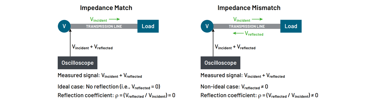
TDR operates based on the principle of electromagnetic wave propagation. Figure 2 illustrates the basic principles. In an ideal scenario, no reflection occurs when an electrical signal travels along a transmission path, ensuring that all signal energy reaches its intended destination without interference. This ideal condition occurs when the impedance of the entire transmission path and the line termination match the output impedance of the signal source. However, even a slight change in the impedance or discontinuity along the path will cause some portion of the incident signal to be reflected back toward the source. The amount of energy reflected is a function of the transmitted energy and the magnitude of the disturbance or impedance change. By analyzing the time taken by these reflections to return and their amplitude, TDR can also determine the location and nature of impedance mismatches or faults.
Transmission lines and characteristic impedance
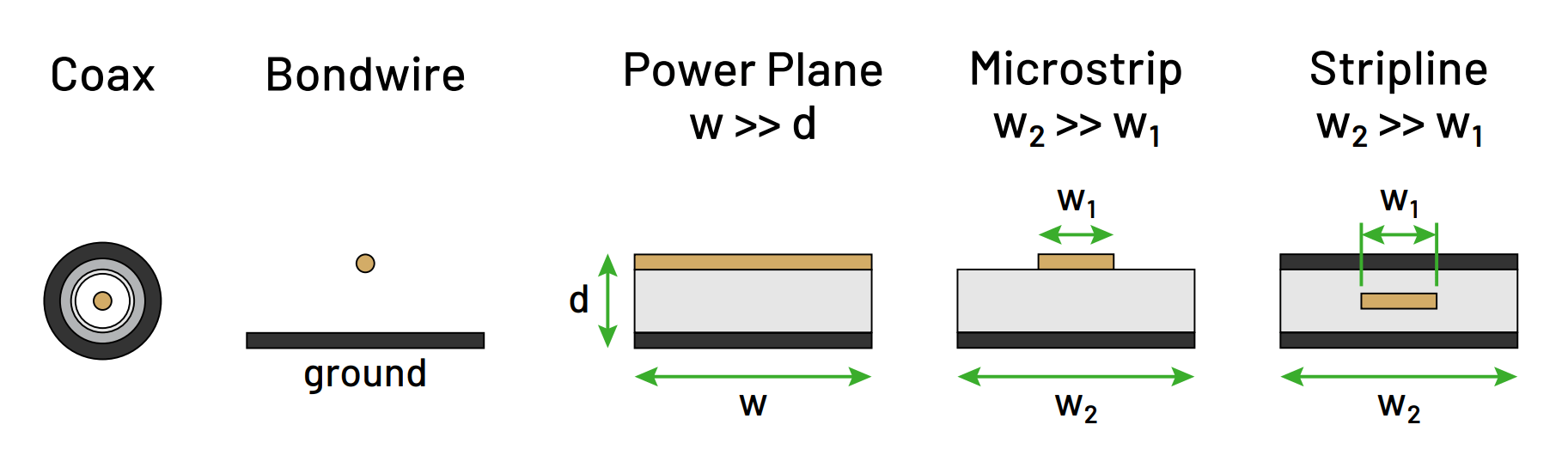
Transmission lines are specialized structures designed to carry electrical signals with minimal loss and distortion. They can take many forms, including PCB traces and vias, cables, connectors, and even on-chip interconnects. Examples of transmission lines are shown in Figure 3.
A transmission line can be first-order modeled by lumped elements such as those shown in Figure 4. Here, the resistance (R), conductance (G), inductance (L), and capacitance (C) are not lumped at a single point but are distributed continuously along the line.
- The series resistance (R) accounts for the Ohmic losses in the conductor
- The dielectric shunt conductance (G) accounts for PCB dielectric loss
- The series inductance (L) represents the magnetic field generated by current flow
- The shunt capacitance (C) represents the electric field generated by the voltages imposed between conductors.
These distributed elements collectively determine the characteristic impedance (Z0) of the transmission line, which influences the signal propagation and signal integrity.
The ideal transmission line does not exhibit losses associated with conductors and dielectrics. Thus, an ideal (lossless) transmission line can be described as a distributed parameter network consisting of capacitors and inductors alone to represent interactions due to electric and magnetic fields. However, real interconnects represent a non-ideal transmission line and exhibit losses. Conductor and dielectric losses are frequency-dependent and normally increase if operational frequency increases. In typical interconnects, the conductor loss dominates at the lower frequencies while the dielectric loss becomes more pronounced at the higher frequencies.
To prevent reflections, transmission lines must be properly terminated. Termination involves matching the impedance of the line to the impedance of the load. Proper termination ensures that the signal is absorbed by the load rather than being reflected along the line, which could cause interference and signal degradation.
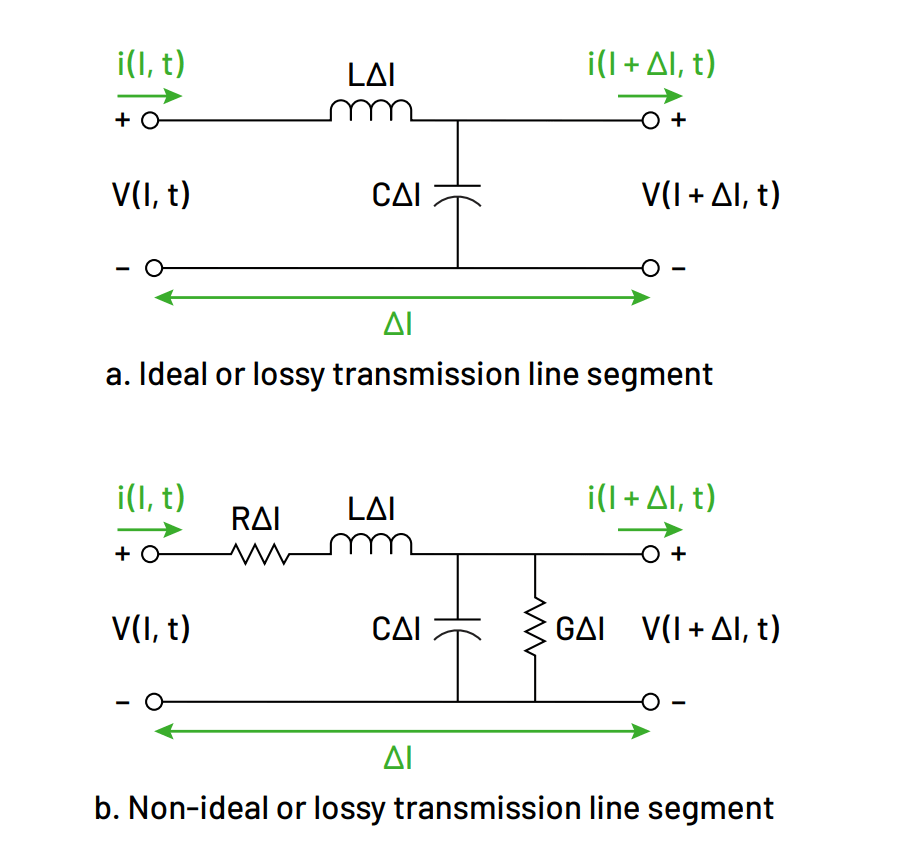
A short sub-segment of the ideal and non-ideal transmission line can be modelled using the circuits shown in Figure 4. Circuit representation of the transmission line allows deriving partial differential equations which are generally called telegrapher’s equations. A solution of these equations in terms for propagating voltages and currents, allows deriving important characteristics of the ideal transmission line, such as characteristic impedance and time delay.
For the single lossless ideal conductor, the characteristic impedance, Z0, is described by the following formula:

And the time delay td per unit length is described by:

For a single lossy conductor, the characteristic impedance, Z0, is described by the following formula:

And the time delay td per unit length is described by:

where
R = series conductor resistance
G= shunt dielectric conductance
L = series inductance
C = shunt capacitance of the transmission line per unit length
ω = angular frequency, given by ω = 2πf, where f is the frequency in hertz
j = the imaginary unit, representing a 90° phase shift
How TDR Works

As noted above and in Figure 5, a TDR system incorporates an inline pulse generator with a fast edge or step. Other architectures using a terminated step source with a power divider are also common; this matters little as long as the signal path is clean.
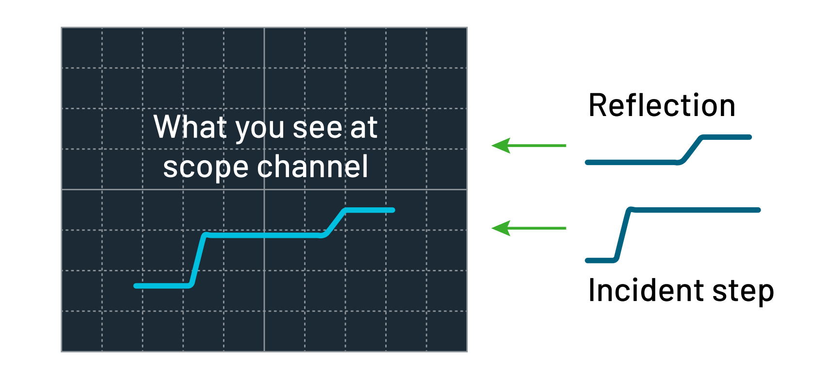
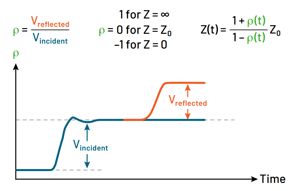
At t=0 the step source produces a step which is sent down the transmission line (DUT) and also to the oscilloscope. The characteristic impedance of the source and cables is generally 50 Ω. Since the oscilloscope is terminated in 50 Ω it causes no reflections. Impedance discontinuities in the DUT, however, will cause reflections. The oscilloscope “sees” both the superimposed combination of the incident voltage (coming from the generator) and the reflected voltage (returning from the DUT) as shown in Figure 6. By analyzing the shape and amplitude of the reflected signal, as compared to incident pulse amplitude, we can determine the magnitude and nature (resistive, inductive, or capacitive) of discontinuities or impedance mismatches. The position of the discontinuity can be determined by measuring the time it takes for the reflected wave to arrive at the oscilloscope and propagation velocity of the pulse within the DUT. It is important to note that time measurements of reflections relative to incident step represent the time required to cover the distance from the source to the discontinuity, and back.
The relationships between the reflected voltage (Vreflected) and the incident voltage (Vincident) can be used to calculate the impedance of the transmission line over its length. The ratio of Vreflected to Vincident is called the reflection coefficient, ρ, where the voltages and ρ are all functions of time:

Note that ρ is dimensionless, and if the DUT is linear, the voltages and step polarities involved with this expression don’t really matter.
If the characteristic impedance of the measurement system is known, the actual impedance of the DUT can be found from the reflection coefficient as a function of time:
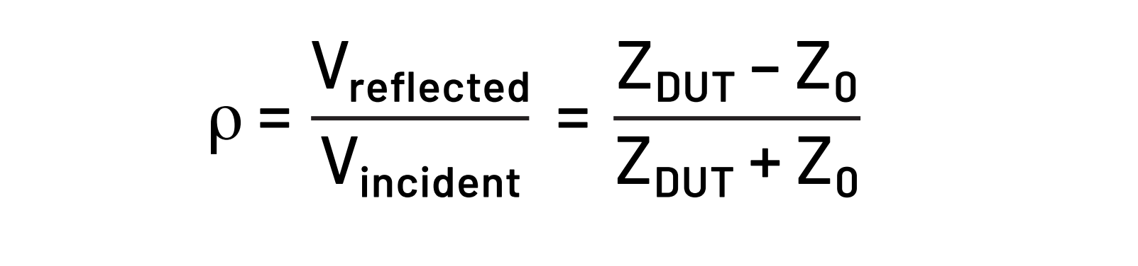
This can be rewritten to find ZDUT based on ρ:

The reflection coefficient (ρ) ranges from -1 to 1 for passive DUTs. A non-zero reflection coefficient indicates an impedance mismatch, which can lead to signal degradation or power integrity issues. A positive ρ indicates a high impedance discontinuity, while a negative ρ indicates a low impedance discontinuity.
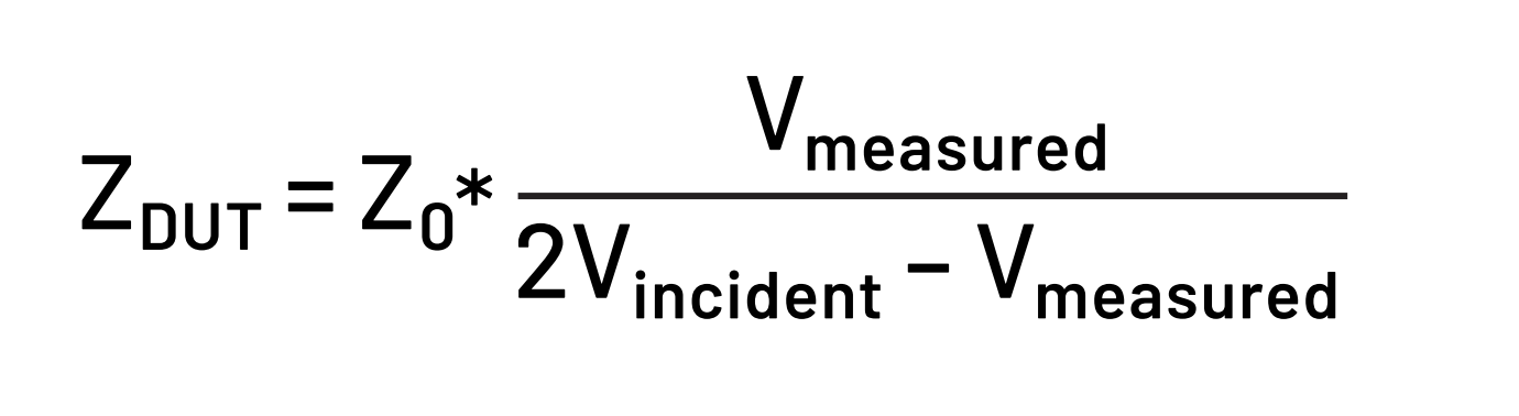
ZDUT can also be expressed in terms of incident and reflected voltages:

Since the voltage measured on the oscilloscope is Vincident + Vreflected, we can express the impedance versus time as:
Opens, Shorts and Mismatches
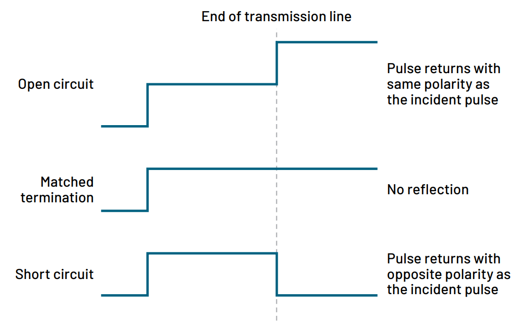
It is helpful to examine a few special cases and note how the reflected voltage, reflection coefficient and impedances behave. The waveforms are shown in Figure 7 and the corresponding scenarios for ρ are shown in Figure 8.
-
Open Circuit: When the transmission line is unterminated, it appears as a complete reflection with maximum amplitude.
Vreflected = +Vincident
Hence, ρ = Vreflected / Vincident = 1
The impedance at the end of the transmission line is practically infinite (open).
-
Matched Impedance: The transmission line is terminated in its characteristic impedance Z0
Vreflected = 0
Hence, ρ = Vreflected / Vincident = 0
The impedance at the end of the transmission line is Z0.
-
Short Circuit: When the transmission line is shorted, it appears as a complete reflection with opposite polarity compared to an open circuit.
Vreflected = - Vincident
Hence, ρ = Vreflected / Vincident = -1
The impedance at the end of the cable is 0 (shorted).
Measuring capacitance and inductance
As previously stated, transmission lines exhibit distributed capacitance and inductance along their length which affect the propagation of electrical signals through the line. TDR techniques can be used to measure capacitance and inductance by analyzing the transmission line’s response to electrical pulses.
When a TDR pulse is sent down a transmission line, changes in capacitance and inductance affect the speed at which the pulse travels along the line and the magnitude of reflections, as manifested by variations in the pulse shape and amplitude.
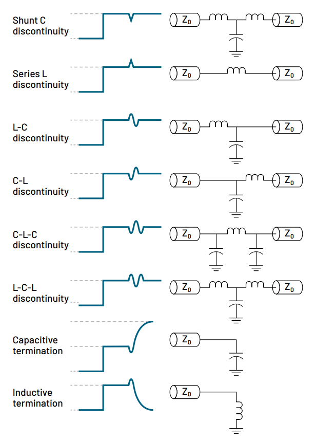
By analyzing the shape, amplitude, and polarity of the reflected signal relative to the incident pulse, engineers can distinguish between capacitive and inductive variations. Figure 9 shows the effects of inductive and capacitive discontinuities. Capacitive variations typically result in downward deflections with faster rise times and lower amplitudes, while inductive variations result in upward deflections with slower rise times and higher amplitudes.
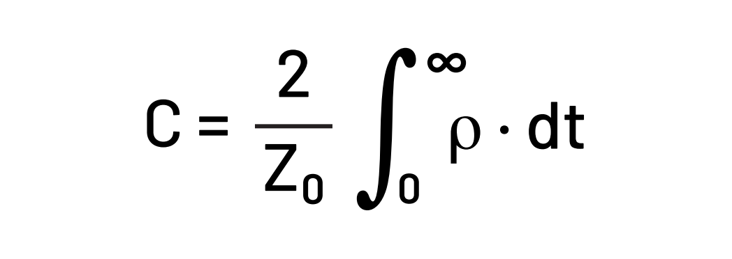
Inline shunt capacitance can be determined from the reflection coefficient ρ, using the equation:
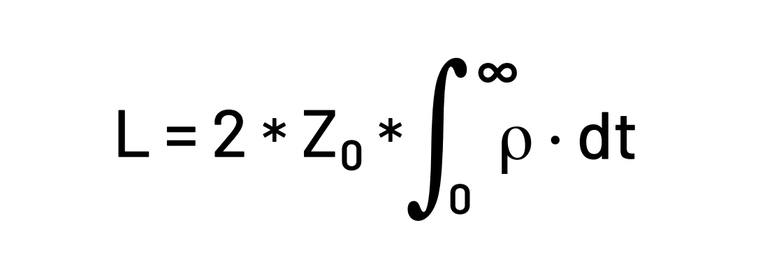
Similarly, inline series inductance may be calculated using this equation:
Making TDR measurements on 4, 5 or 6 Series MSO oscilloscopes
As the name suggests, TDR is a time-domain technique and employs oscilloscopes for signal measurement and analysis. Sampling scopes are often used, since they have excellent time resolution. However, real-time oscilloscopes are more commonly used in debugging and validation, so it is valuable to be able to apply TDR techniques using these “everyday” oscilloscopes.
The available 10 GHz bandwidth on the 6 Series MSO makes it a good choice for TDR. (See “Appendix A. The Effect of Bandwidth on TDR” to better understand the relationship between measurement system rise times and TDR resolution.)
For the stimulus, a pulse/step generator is needed. A single source is used for single-ended measurements and a dual source is used for differential measurements. The ideal generator can produce very fast edges (i.e., small rise and fall time). To avoid measurement system artifacts highquality cables and power splitters are needed. The Picotest J2154A TDR source has a built-in splitter and supports both single-ended and differential TDR measurements.
Application software on the oscilloscope facilitates calibration, setups and measurements.
For this primer, the following instruments are used:
- Tektronix 6 Series B MSO with 10 GHz bandwidth, equipped with Option 6-TDR Time Domain Reflectometry Measurement and Analysis software
- Picotest J2154A PerfectPulse® Differential TDR with integrated step generator
- Matched 50 Ω cables
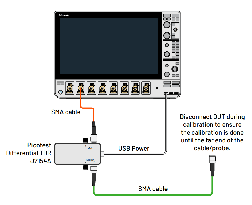
A typical TDR setup utilizing a DUT, Picotest TDR unit J2154A and 6 Series MSO real-time oscilloscope from Tektronix is shown in Figure 10.
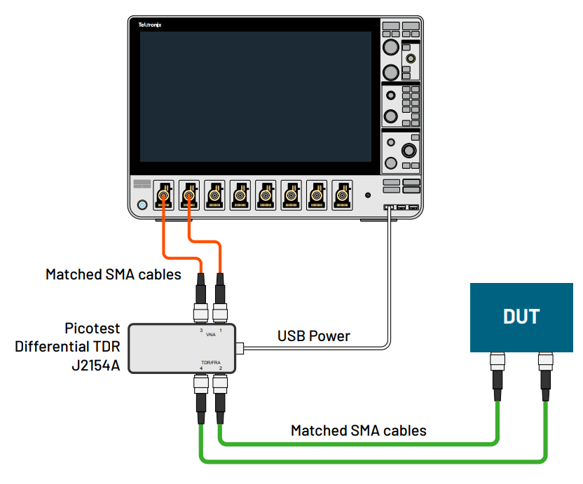
When conducting TDR measurements with an oscilloscope, engineers can choose between single-ended and differential probing techniques. Single-ended probing involves connecting one probe to the signal line, while differential probing requires two probes to measure the voltage across a differential pair. A differential impedance measurement enables engineers to analyze various aspects of signal integrity, such as common-mode noise rejection. In addition, differential TDR is very useful for two-port characterization, whether it is crosstalk between two single-ended traces or coupling between differential pairs.
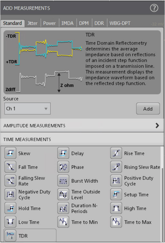
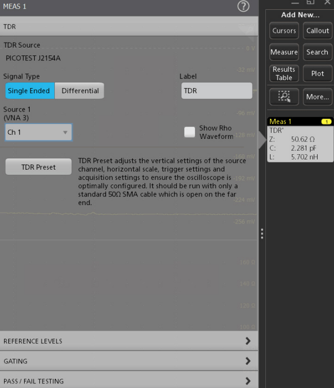
The 6 Series MSO can be equipped with Option 6-TDR Time Domain Reflectometry Measurement and Analysis software. This software facilitates configuration, calibration, calculations and scaling. It also produces measurements. Once installed, the TDR measurements appear as part of the Time Measurements group, as shown in Figure 12. Once the TDR measurement is added, double-tapping on the measurement badge brings up the configuration shown in Figure 13. The software supports both single-ended and differential TDR measurements using the Picotest J2154A as a pulse generator.
Preparing to Make TDR Measurements: Preset and Calibration
Configuring the oscilloscope and normalization are important steps before performing actual measurements.
The entire system, up to the probe tip or cable end must be calibrated to remove measurement system effects to focus only on impedance changes in the DUT. Traditionally, TDR systems have been calibrated with open, load, and short connections. However, the TDR Measurement and Analysis software on Tektronix MSOs allows compensation in a single step, using information gathered from the incident and reflected waveform. The TDR Preset function in the TDR Measurement and Analysis software automatically configures the oscilloscope settings and normalizes the rho waveform.
Configuring the Oscilloscope
Before performing actual calibration, one must set the scope channel to 50 Ω termination, and make sure the horizontal scale and sample rate are set to capture the best signal. Also, the vertical scale must be set to make sure the signal is acquired with the best accuracy. Waveform averaging helps to improve vertical resolution and the software configures the scope to average 20 TDR waveforms per test. All these steps are performed by clicking on the TDR Preset button. Once the oscilloscope is configured, the preset function normalizes the reflection coefficient (ρ) waveform.
TDR Normalization
TDR normalization is an important step before performing the TDR measurement. During normalization, any signal offsets and amplitude errors are corrected.
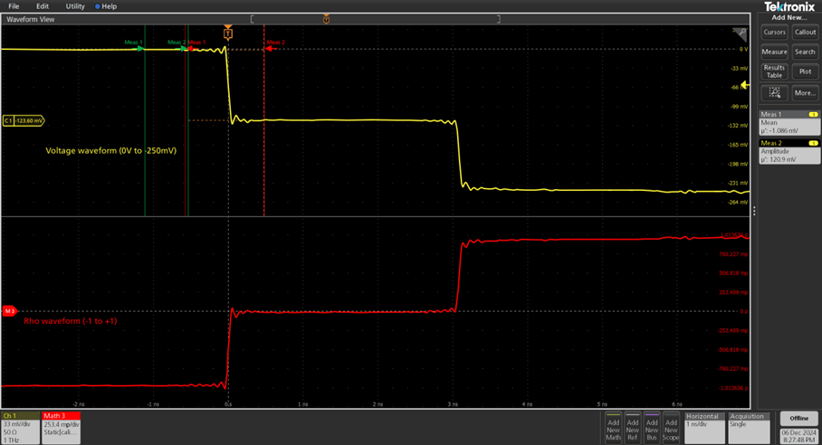
The equation to calculate the ρ waveform from the voltage waveform is: ρ(t) = ( v(t) – Vmean ) / Vamp
where:
v(t) = the voltage samples from the incident + reflected waveform
Vmean = the mean value of the voltage waveform before 1st reflection.
Vmean is measured in the Z0 region indicated by Meas1 in Figure 15.
Vamp = the amplitude of the incident step voltage waveform. Vamp is the amplitude of the waveform as described by Meas2 annotations in Figure 15.
Note that the incident voltage waveform from the Picotest J2154A pulse generator is a negative pulse. The calculations are made accordingly.
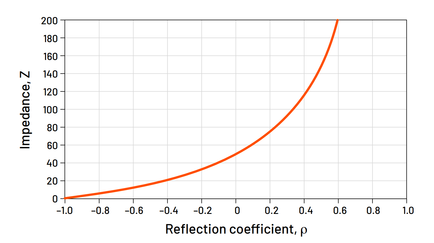
Due to the inherently non-linear relationship between ρand impedance (Z), shown in Figure 16, even minor errors in the ρ waveform can lead to significant inaccuracies in the resulting impedance waveform. Hence proper normalization is a must.
After normalization, the Rho waveform ρ(t) is created as shown in the lower waveform in Figure 15. The input signal will be a negative step starting from 0 V (short) to –125 mV (load) and –250 mV (open circuit). On the Rho scale, these waveforms are transformed to a –1 to +1 range, where –1 ρ represents a short circuit, 0 ρ represents a 50 Ω load, and +1 ρ represents an open circuit.
TDR Examples and Application Areas
These examples have all been developed using a 6 Series B MSO with 10 GHz bandwidth.
Example 1: Measuring a 50 Ω microstrip with correction
The microstrip shown in Figure 17 was designed to hit a target of 50 Ω.
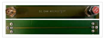
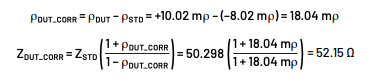
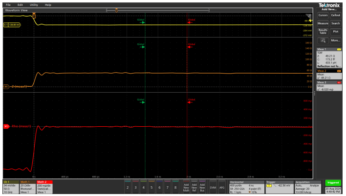
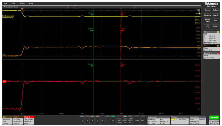
In this example, the average impedance of such a constant-width microstrip line is measured employing a correction technique against a standard reference that is outlined in IPC-TM-650, method 2.5.5.7 subsection 5.2.1 [6]. This technique may be used to improve the accuracy of a 50 Ω microstrip. The nominal 50 Ω standard reference was first verified to be ZSTD_TRACE = 50.298 Ω when checked with a traceable DVM. Both the 50 Ω standard reference and the microstrip were checked using TDR and employing a mean measurement over exactly the same gated measurement zone, as required by subsection 5.2.1 of the IPC standard. The following values were measured over the 30%–70% reflection zone of the line:
standard reference: ZSTD = 49.21 Ω and ρSTD = -8.020 mρ (see Figure 18)
microstrip line: ZDUT = 51.02 Ω and ρDUT +10.02 mρ (see Figure 19)
Using these values as outlined in subsection 5.2.1 of the IPC standard, the corrected characteristic impedance of the microstrip is 52.15 Ω:
Example 2: Finding Impedance Discontinuities using TDR
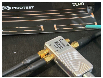
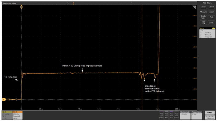
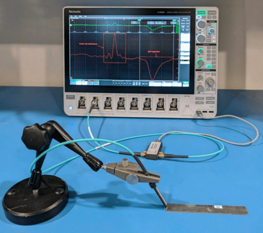
One can see the 50 Ω trace associated with the P2105A probe after the first reflection. Minor glitches at the beginning and end of the cable indicate contact impedance mismatches.
To the right of the probe connection, two impedance discontinuities are visible in the impedance waveform. The two negative blips correspond exactly to wider sections in the PCB traces. By enabling the measurement cursors and placing the cursors across these blips, we can measure the impedance of these locations. PCB trace designers usually aim to make trace width consistent and can use TDR measurements to find unexpected discontinuities.
In addition, one can determine the distance between these discontinuities by measuring the timing difference between these points and using the dielectric constant of the trace.
Example 3: Measuring a 1 pF shunt capacitor
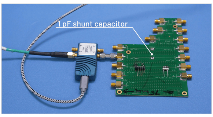
Figure 22 shows a PCB with a trace on which a 1 pF shunt capacitor is soldered. We want to measure the impedance of the entire trace and look at the effect of the capacitor in the path. Figure 23 shows this measurement. There is a negative blip on the impedance trace due to the capacitor in the path.
We can easily measure the capacitance value by integrating the area within the blip in rho-seconds and dividing by the reference impedance (Z0) as:
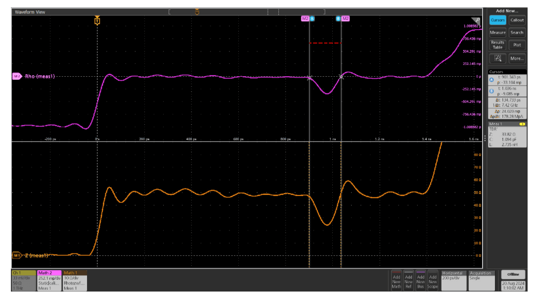
The TDR measurement in the badge does this automatically as we enable cursor gating for the measurement and place the cursors across the capacitive region on the trace. The inductive blip after the capacitor is due to the parasitic inductance in the capacitor. To accurately measure the capacitance, one must carefully place the cursors in the correct region. One easy way to set the region is by choosing those locations where the rho waveform crosses zero value on both the sides, which will gate just the capacitive region, ignoring the inductive region after the capacitive region. This measurement gives a value of 1.094 pF which is very close to the nominal value of 1 pF.
PCB designers use capacitance measurements to characterize losses across the PCB trace due to capacitive and inductive regions along the trace.
Example 4: Measuring a Series Inductor
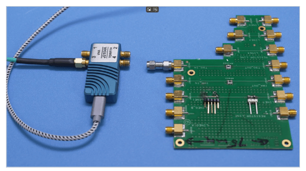
Like the capacitance measurement, inductance can also be measured from the TDR waveform. On the same board used in the previous example, we have a 2.6 nH inductor soldered in series with the PCB trace path at the halfway point between the connector launches as shown in Figure 24.
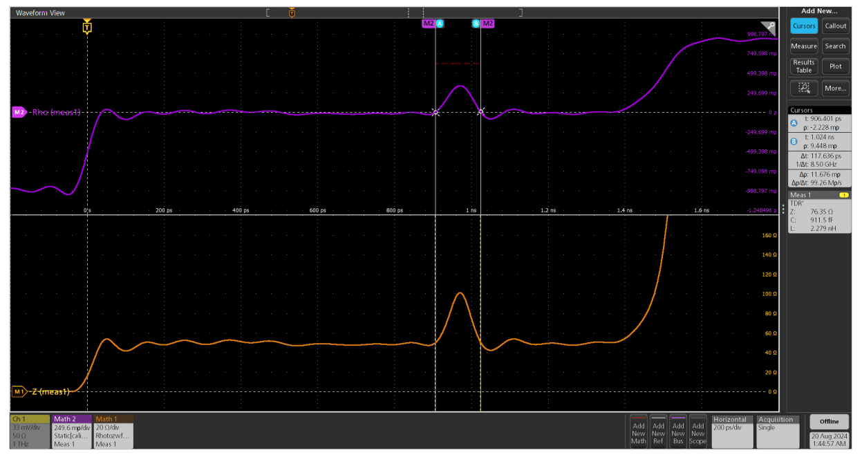
Figure 25 shows the impedance trace measured on the scope. You can see a positive blip due to the inductor in between the cursors. The inductance value can be computed by integrating the area within the blip in rhoseconds and multiplying by reference Impedance (Z0) as below:

The inductance value is automatically calculated in the TDR measurement based on the placement of cursors across the inductive region. We are measuring a value of 2.279 nH, and we expected 2.6 nH of inductance value based on the manufacturer’s value for the part. The reason for seeing less inductance here is the parasitic capacitance effects of both end plates to ground, as well as bridging capacitance around the part. While these won’t contribute significantly at the low frequency impedance bridge measurements used by the part manufacturer, it does matter to the fast TDR edge used in this test — which better represents the actual environment experienced by real signals with higher edge rates. At some frequency, in fact, the capacitive parasitics will cause a self-resonance within the part, rendering the part ineffective as an inductor.
Example 5: Using TDR to Measure the Impedance of an IC Output
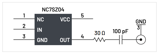
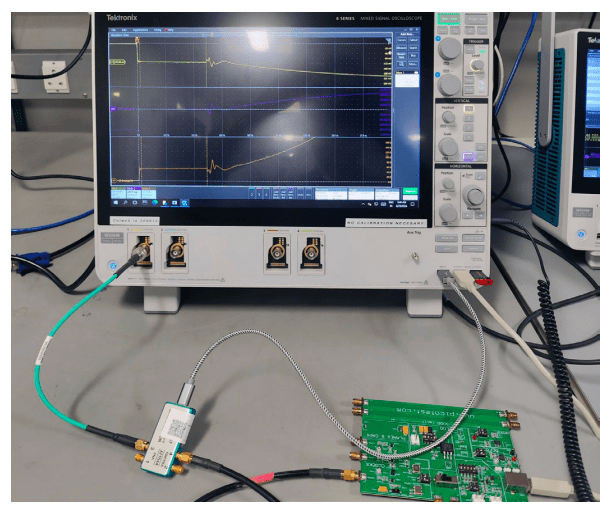
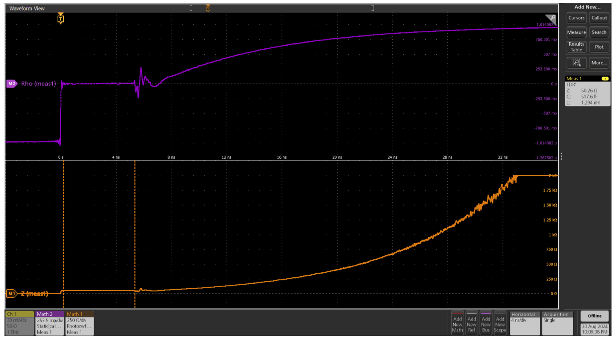
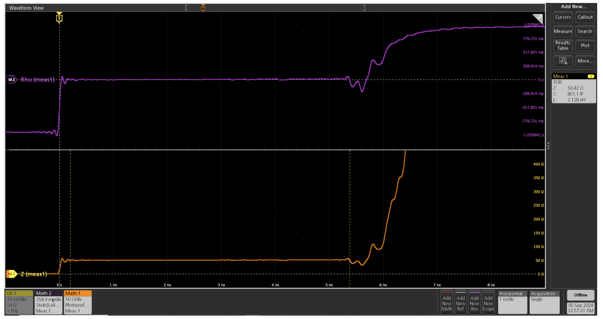
In the first test, the IC is powered but its input is not being driven. As seen from the impedance trace in Figure 28, the 30 Ω resistor and the 100 pF in series with the TDR system’s 50 Ω impedance, produces an approximately 8 ns RC time constant. This can be estimated by observing the time to reach a Rho value of 1-e–1 = 63.2%, or r = 0.632.
The nominal value of the RC time constant is calculated as below:

Now, with the clock output switched OFF, the measured TDR signal is shown in Figure 29. As we see from the TDR signal, the gate’s loading effect is merely a shunt capacitance only. This is because the output impedance of the inverter will be very high and it acts like an open circuit along with the series 30 Ω resistor.
Summary
TDR is a valuable tool for analyzing and characterizing transmission lines. From assessing power rails on PCBs to analyzing cable integrity, TDR impedance measurements provide engineers with critical insights to optimize their PCB designs.
While sampling oscilloscopes are often used for TDR, general-purpose, real-time oscilloscopes are more broadly available and are effective instruments for performing TDR analysis along with an appropriate step source and analysis software.
Appendix A. TDR Resolution on a Real-Time Oscilloscope
Vertical Resolution
Vertical TDR resolution is the measure of how small an impedance variation one can measure. The maximum sensitivity of J2154A with 6 Series MSO can be derived as below:
Resolution of reflection coefficient and impedance per division at 10 mV/div scale:
Since the J2154A is a 250 mV step generator, the voltage scale ranges from -125 mV to +125 mV. On the rho scale, this corresponds to -1 to +1. Hence, the vertical sensitivity at 10 mV/div corresponds to 80 mρ /div on the reflection coefficient scale. Most impedance measurements are around 50 Ω. Due to the nonlinear relationship between impedance and ρ (refer to Figure 16 above), an 80 mρ/div sensitivity in ρ corresponds to 8 Ω/div near 50 Ω.
Maximum vertical resolution at 50mV/div scale:
At 50 mV/div vertical scale, which is the most common scale for TDR measurements, the maximum vertical resolution with the 12-bit analog-to-digital converter (in High Res mode) in the 6 Series B MSO can be calculated:
- With 12 bits resolution and 50 mV/div, full scale is 500 mVpp which is represented by 4096 ADC levels.
- One LSB in Volts is therefore 500 mV/4096 = 125 µV/LSB (rounding a bit to keep this simple).
- A TDR incident edge is 125 mV on the Picotest J2154A.
- This is scaled to 1000 mρ.
- One LSB in Rho is therefore (1000 mρ / 125 mV) * 125 µV/ LSB = 1 mρ/ LSB.
Hence, we can say that the maximum resolution at 50 mV/div scale is 1 mρ/LSB, or 0.1 Ω/LSB at around 50 Ω. Resolution improves to 62.5 μρ/LSB, or 6.25 μΩ/LSB near 50 Ω operation if we use high resolution mode, which provides 16 bits. But we have to decrease the sample rate to 125 MS/s to achieve 16 bits of ADC resolution.
Resolution with Averaging:
Another way to improve the resolution is by using waveform averaging. Performing 16 waveform averages effectively improves the resolution by 2 bits which in turn reduces random noise and improves accuracy.
In summary, both the ρ and Z waveforms are math traces and can be set up to resolve differences below 1 mρ or 0.1 Ω.
TDR horizontal resolution
TDR resolution determines the detail available in impedance discontinuities. TDR gives a measure of impedance versus time, and time is directly proportional to physical distance. We can convert the x-axis to distance and view the impedance versus distance curve, which gives us a clear indication of the location of impedance mismatches. This helps in finding the length of a cable, distance to a cable fault, or the location of a discontinuity on a trace.
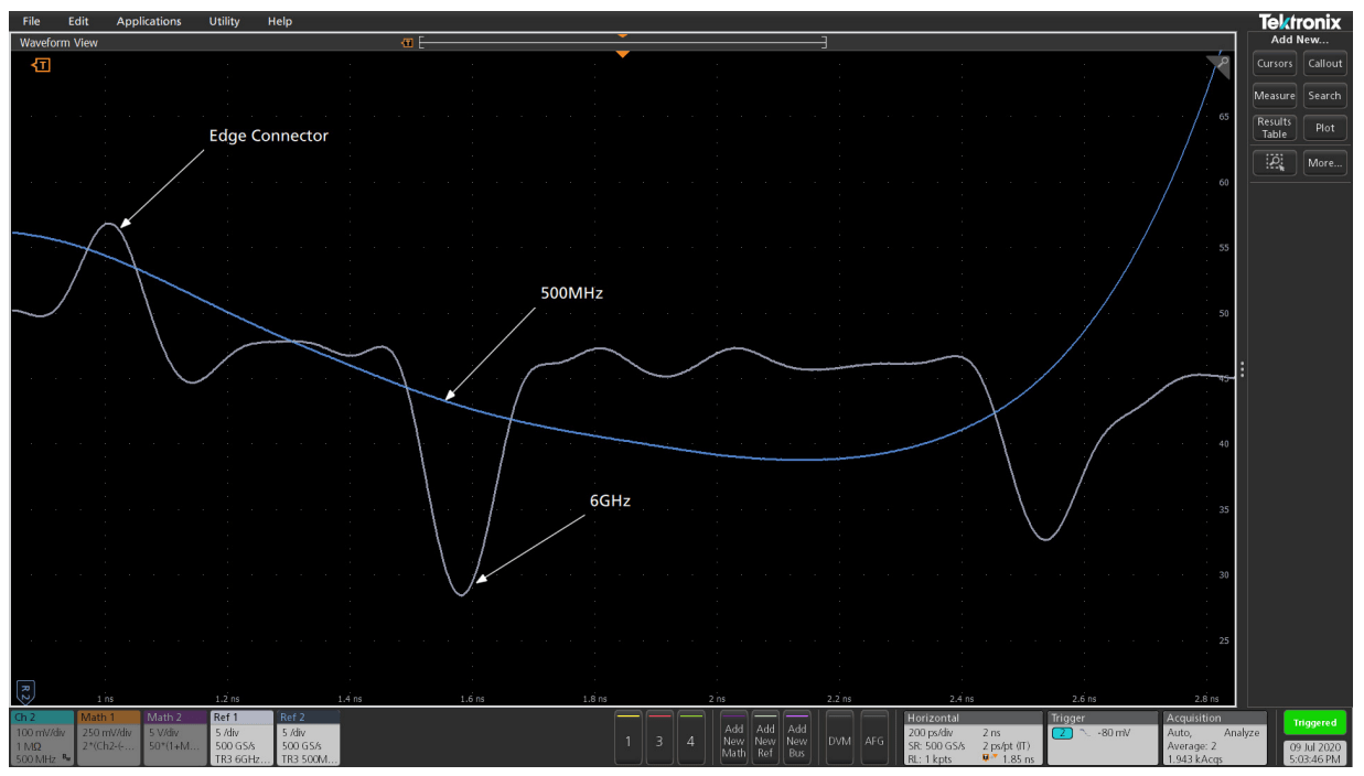
TDR resolution depends on the system bandwidth, which determines the minimum rise-time the measurement system can resolve. This is illustrated in Figure 30, in which TDR measurements are taken using systems with 500 MHz and 6 GHz bandwidths. The lower bandwidth system is not able to resolve impedance discontinuities that are clearly visible on the higher bandwidth system. System rise-time and the transmission line’s velocity of propagation can be used to find the minimum resolvable distance.
TDR signal propagation delay:
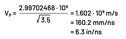
The speed of electrical signal in air is same as speed of light, but in a medium it depends on the effective Dk of the medium.
Speed of light in vacuum is c = 2.99792468 * 108 m/s
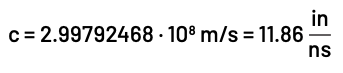
The velocity/speed of electrical signal (Vp) in a medium is:
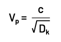
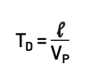
The propagation delay (tD) for the signal to travel a distance L will be:
For a PCB trace, with a dielectric constant (Dk) of 3.5:
So for a PCB trace, the time delay for 1 mm will be:
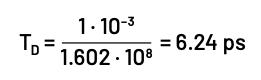
The propagation delay seen by the scope will be a round-trip delay, which will be 2 * 6.24 ps = 12.48 ps.
TDR System Bandwidth:
Note that the TDR system bandwidth depends not only on the oscilloscope. The step generator and TDR probes or cables will also contribute to the system risetime. As the system risetime increases, the minimum TDR resolution will also increase. Total system risetime is:

where:
trTDR = the TDR step generator rise time or fall time, 10% to 90%
trscope = the oscilloscope rise time or fall time, 10% to 90%
trprobe = the probe rise time or fall time, 10% to 90%
Using the system rise time, we can easily find the resolution limit.
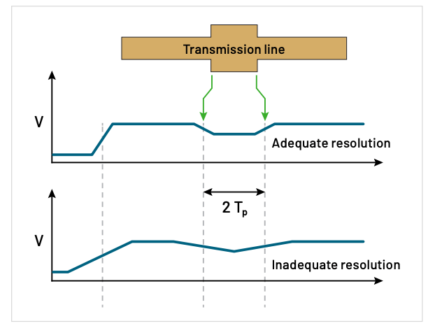
As per IPC-TM-650 Test Methods Manual [6], the TDR resolution limit is defined as:

TDR Resolution Example
Assuming a transmission line has a dielectric constant, Dk = 3.5, the velocity of propagation VP will be 6.33 in/ns. The P2105A probe has a bandwidth of 16.5 GHz. We can calculate the probe’s rise time as 0.35/bandwidth = 0.35/16.5 GHz = 21.21ps. For the J2154A TDR, trTDR = 30 ps. For the 6 Series MSO scope, trscope = 40 ps.
For the P2105A TDR probe, trprobe = 21.21 ps. So system rise time will be:


Note: This resolution can be achieved in the ideal case with 3.5 as a dielectric constant(Dk). But in practical cases, the effective dielectric constant of the conductor would be lower than 3.5 as energy flows on the outer surface of the conductor. Hence an effective value needs to be considered for practical calculations. Refer to the Picotest application note [1] in the References section.