
Introduction
Semiconductor materials used in power electronics are transitioning from silicon to wide bandgap semiconductors such as silicon carbide (SiC) and gallium nitride (GaN) due to their superior performance in many applications. Wide bandgap switching devices enable smaller, faster and more efficient designs. The power-density advantages of smaller and lighter designs are particularly evident in space constrained and mobile products such as electric vehicles, but compact power electronics are desirable across a wide range of products. At the same time, efficiency is increasingly important as governments introduce financial incentives and more stringent energy-efficiency regulations.
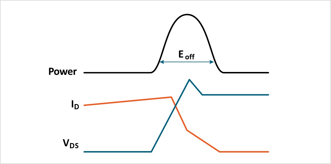
When designing power converters, a 0% power loss is ideal as illustrated in Figure 1. However, switching losses are inevitable. So, the goal is to minimize the losses through design optimization, and design parameters related to efficiency must be rigorously measured.
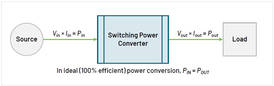
A traditional silicon-based converter might have an efficiency of about 87% to 90%, meaning that 10% to 13% of the input power is dissipated within the converter, mostly as waste heat. A significant portion of this loss is dissipated in the switching devices such as MOSFETs or IGBTs. [2]
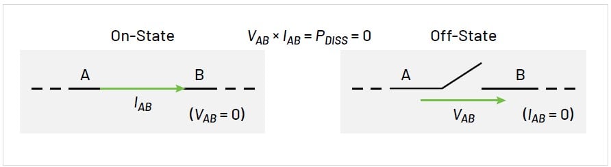
Ideally, the switching device is either “on” or “off” as shown in Figure 2 and instantaneously switches between these states. In the “on” state, the impedance of the switch is zero ohms and no power is dissipated in the switch, regardless of how much current is flowing through it. In the “off” state, the impedance of the switch is infinite, and zero current is flowing, so no power is dissipated.
In practice, power is dissipated during the transition between “on” and “off” (turn-off) and between “off” and “on” (turn-on). These non-ideal behaviors occur because of parasitic elements in the circuit. The parasitic capacitances on the device , shown in Figure 3, slow the switching speed of the device, extending the turn-on and turn-off times. [2] In order to keep the switching losses at minimum and thus design more efficient converters, design engineers simulate and measure switch timing and associated energy losses.

Engineers also measure energy loss due to reverse recovery. This loss is caused by a transient current flowing into the switching device as the diode feeding it switches from being forward-biased to reverse-biased.
The preferred test method to measure the switching parameters of MOSFETs or IGBTs is the “Double Pulse Test” method. The test methods are described in JEDEC and IEC standards, including JEP182 [3], JESD24-10, IEC 60747-9, IEC 60747-8 and IEC 60747-9.
This application note will describe double pulse testing and how it’s implemented using instrumentation. It will cover switching loss and reverse recovery measurements. In particular, it will explain how to generate pulses with the Tektronix AFG31000 Arbitrary Function Generator and measure important parameters with a 4, 5 or 6 Series MSO oscilloscope and probes.
What is the Double Pulse Test?
Double pulse testing (DPT) is a method to measure the switching parameters and evaluate the dynamic behaviors of power devices. It enables engineers to test switching devices under controlled voltage, current and temperature conditions. Pulses are used to limit self-heating of the DUT and maintain a stable junction temperature. This test is performed to:
- Guarantee specifications of power devices like MOSFETs and IGBTs.
- Confirm actual value or deviation of power devices or power modules.
- Measure switching parameters under various load conditions and validate performance across many devices. [3]
The goals of this testing are typically to measure the following switching parameters: [4][5]
- Turn-on Parameters:
- Turn-on delay, td(on)
- VDS fall time, tf
- Turn-on time, ton
- Max drain current, ID
- dv/dt
- di/dt
- Turn-on energy, Eon
- Dynamic RDS(on)
- Turn-off Parameters:
- Turn-off delay, td(off)
- VDS rise time, tr
- Turn-off time, toff
- Max drain to source voltage, VDSM
- dv/dt
- di/dt
- Turn-off energy, Eoff
- Output charge, Qoss
- Reverse Recovery Parameters:
- Reverse recovery time, trr
- Reverse recovery current, Irr
- Reverse recovery charge, Qrr
- Reverse recovery energy, Err
- di/dt
- Forward on voltage, VSD
A typical Double Pulse Test circuit is shown in Figure 4.
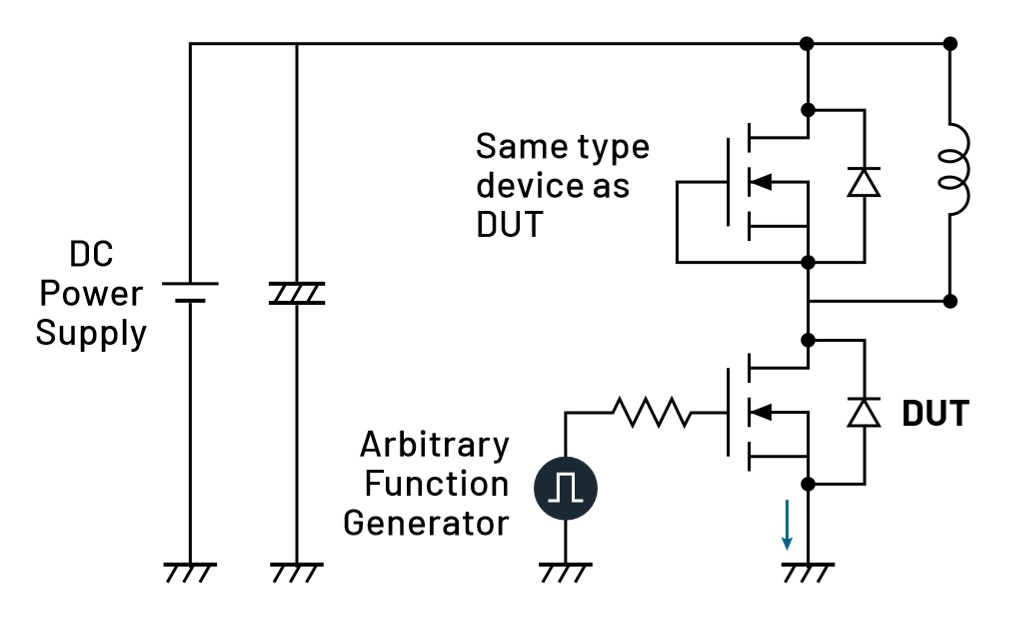
The test is most often performed with an inductive load and a power supply, although the exact circuit may vary depending on the intended application of the power devices under test. [3] The inductor is used to replicate circuit conditions in a converter design. The power supply is used to provide voltage to the inductor. An arbitrary/function generator is used to generate pulses to trigger the gate of the MOSFET to turn it on and off.
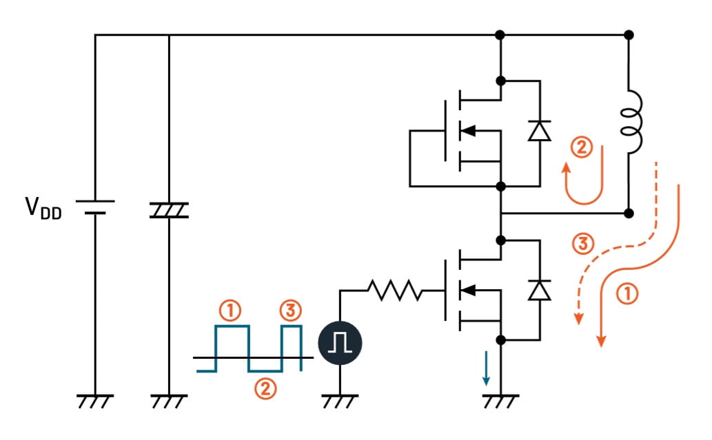
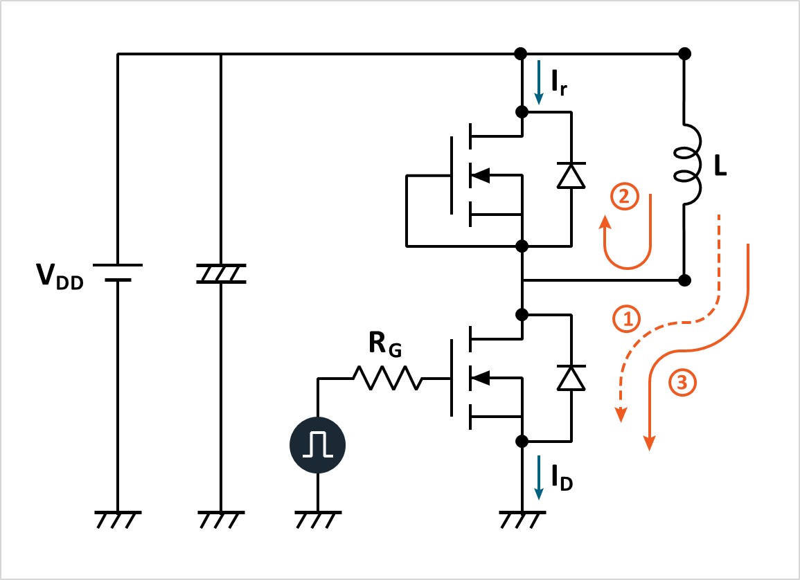
Figure 5 shows the current flow within the different stages of the test for a DPT with MOSFETs. The same current flow would apply when testing IGBTs as shown in Figure 6.
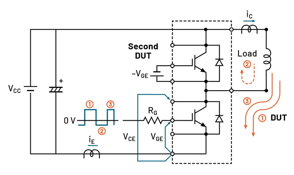
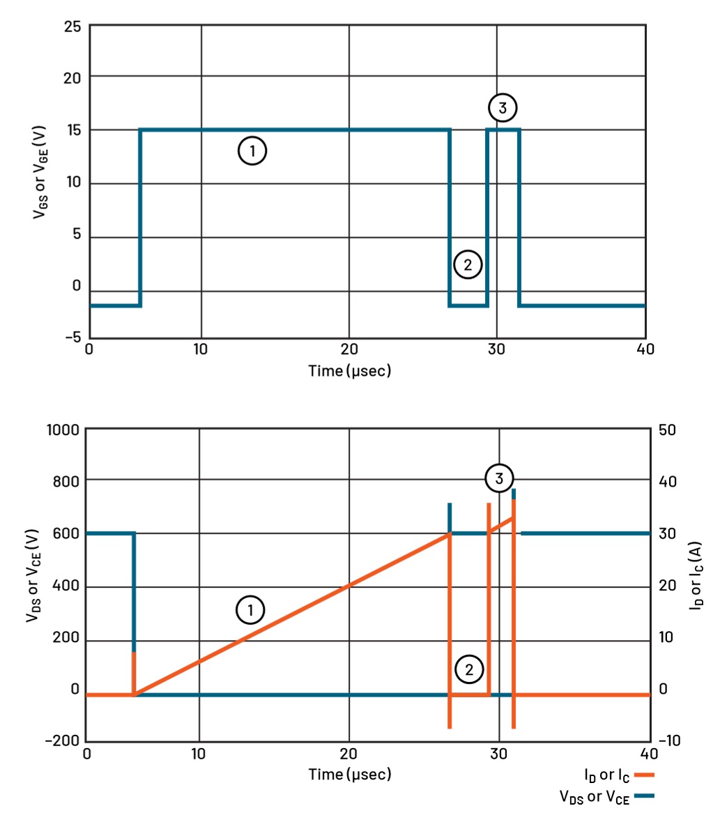
Figure 7 shows typical double pulse test waveforms for a low-side MOSFET or IGBT. There are three important stages of a typical DPT. These stages are represented in Figures 5, 6 and 7 and described here:
- Establish the target test current (Id). The width of the first pulse is adjusted to deliver the desired test current through the load inductor.
- Turn-off of the first pulse and turn-off measurements. At this point ID has reached the desired test current and drops to zero as the power device turns off. Turn-off delay (td(off)), fall time (tf), turn-off time (toff), Off Energy (Eoff), dv/dt and di/dt. A load current flows from the load inductor through the free-wheeling diode. The turnoff period is kept short to keep the load current to the target ID.
- Turn-on of the second pulse and turn-on measurements. This is where turn-on measurements are taken as the target ID starts to resume its flow into the power device. The current overshoot during this turn-on is due to temporary excess current during the reverse recovery of the free-wheeling diode. The second pulse width is kept just long enough to ensure stable measurements while avoiding excessive heating.
Turn-off and Turn-on Measurement Definitions
In order to calculate turn-on and turn-off parameters, we focus on the first turn-off of the switching device and the subsequent turn-on. At these points ID should be at the target current level for the test.
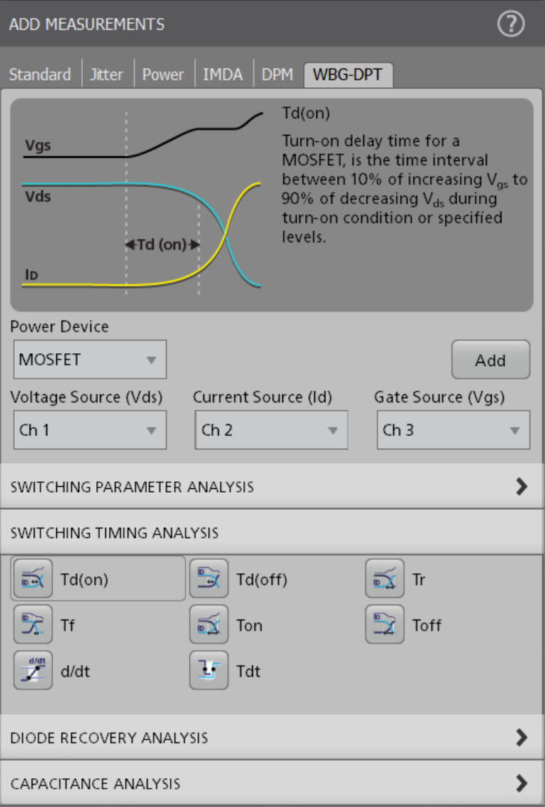
The industry standard definitions for turn-on and turn-off timing parameters are illustrated in Figure 8.
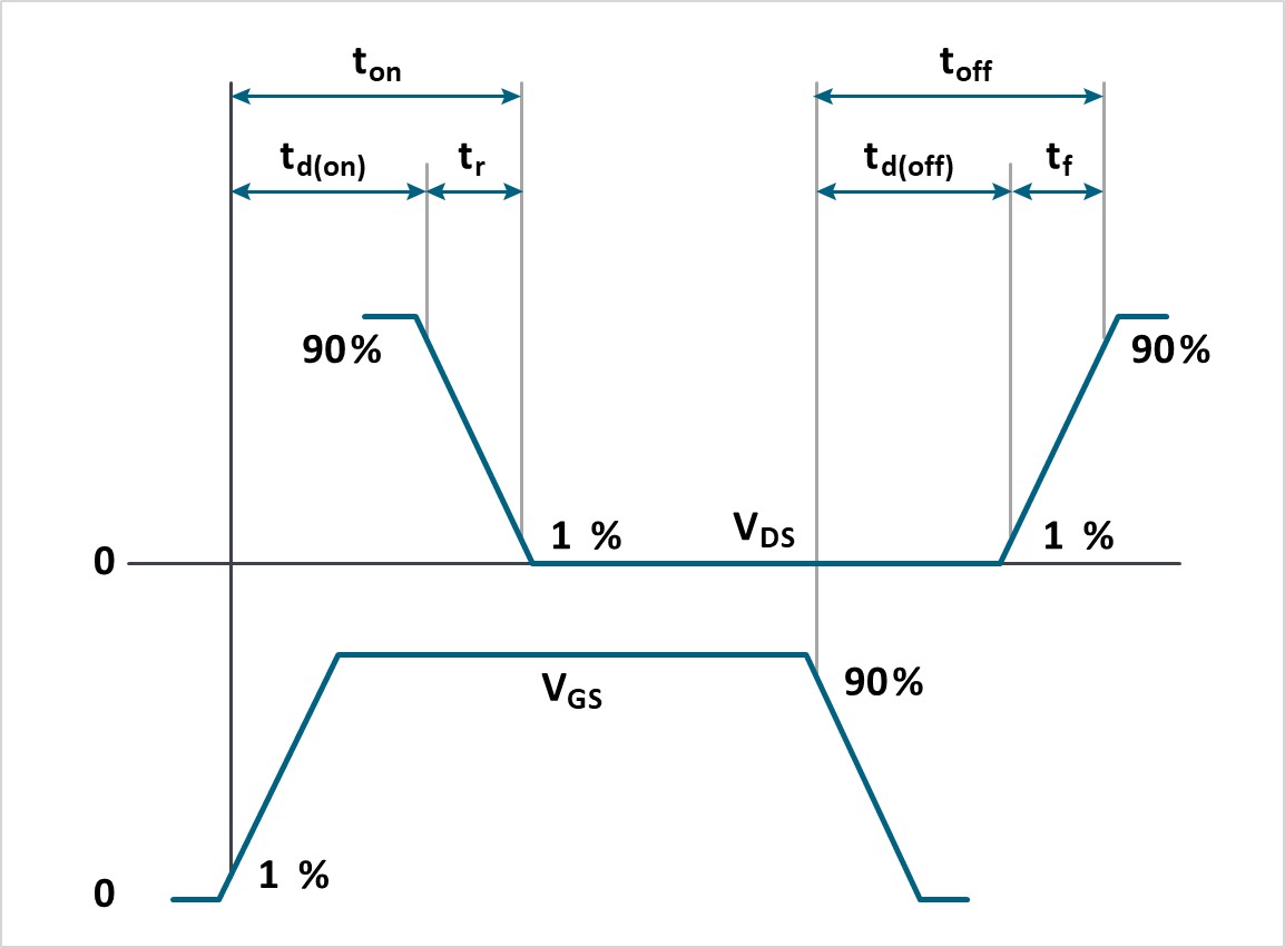
- td(on): Time interval between VGS at 10% of its peak and VDS at 90% of its peak amplitude.
- tr: Time interval between VDS at 90% and 10% of its peak amplitude. Note that tr is measured when the device turns on, thus on the falling edge of VDS.
- td(off): Time interval between VGS at 90% of its peak and VDS at 10% of its peak amplitude.
- tf: Time interval between VDS at 10% and 90% of its peak amplitude. Note that tf is measured when the device turns off, thus on the rising edge of VDS
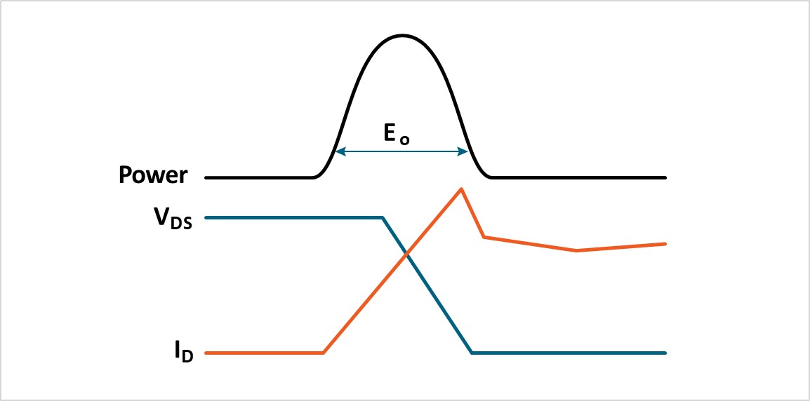
To calculate energy loss, instantaneous power is calculated and then integrated to find energy. Turn-on loss is measured by integrating power dissipation during turn-on (Figure 9, Equation 1):

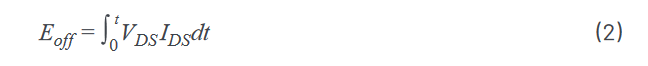
The same approach is used to calculate energy losses during the turn-off transition (Figure 10, Equation 2):
The math for these calculations can be performed on the oscilloscope by combining waveform math to multiply the VDS and ID waveforms to build a power waveform and then using an area (integration) measurement to find energy, gated to measure during turn-on and turn-off. The calculations can also be performed on waveform data by using math software such as MATLAB. In this app note, calculations will be performed using measurement algorithms built into the WBG-DPT oscilloscope application.
Reverse Recovery Measurements
In addition to turn-on and turn-off losses, it is also important to understand losses associated with diode reverse recovery. Reverse recovery current flows through a diode for a short duration, whenever the diode switches from forward biased (on) to reverse biased (off).
The reverse recovery measurement is performed on the free-wheeling diode in the test setup. In Figure 11, the high-side diode is free-wheeling when the low-side diode is turned off during Stage 2. As the low-side MOSFET turns on again and Stage 3 begins, the high-side diode would ideally block reverse current immediately. However, a real diode conducts briefly before turning off. The reverse recovery current translates into energy loss, which impacts the efficiency of the power converter.
Reverse recovery parameters are shown in Figure 12 and include Trr (reverse recovery time), Irr (reverse recovery current), Qrr (reverse recovery charge), Err (reverse recovery energy), di/dt, and Vsd (forward on voltage).
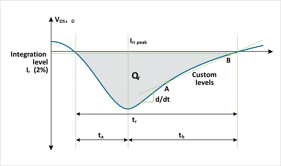
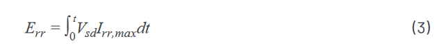
Equation 3 is used to calculate the energy losses during the transition:
Double Pulse Test Setup
Warning! Since power semiconductor tests can involve lethal voltages and currents, it is vital that appropriate enclosures with safety interlocks and personal protective equipment be used!
An example of the instrumentation for double pulse testing is shown in Figure 13. The general setup includes:
- A signal source to provide gate drive signals, usually through an isolated gate driver. The widths of each pulse must be independently variable. Because of this an arbitrary/function generator (AFG) is commonly used and special DPT software is valuable for setting up the stimulus. The AFG may be a standalone instrument such as the AFG31000 Series or built into the oscilloscope such as those available on 4, 5 and 6 Series MSOs.
- A DC power supply to deliver sufficient drain voltage (VDD) and drain current (ID) for testing. Examples include the EA-PSI 10000 programmable power supply for testing at up to 2 kV and 30 kW, the Keithley 2657A High Voltage Source Meter Unit (SMU) for testing up to 3 kV, or the Keithley 2260B-800-2, programmable DC power supply for testing up to 800 V.
- A DC power supply for any supporting electronics such as gate drive ICs. Examples include the Keithley Series 2230 or Series 2280S DC power supply.
- A multi-channel digital oscilloscope to acquire and measure VDS, VGS, and ID. This application note describes testing with a Tektronix 5 Series B MSO, but a 4 Series B MSO and 6 Series B MSO operate the same albeit with different specifications.
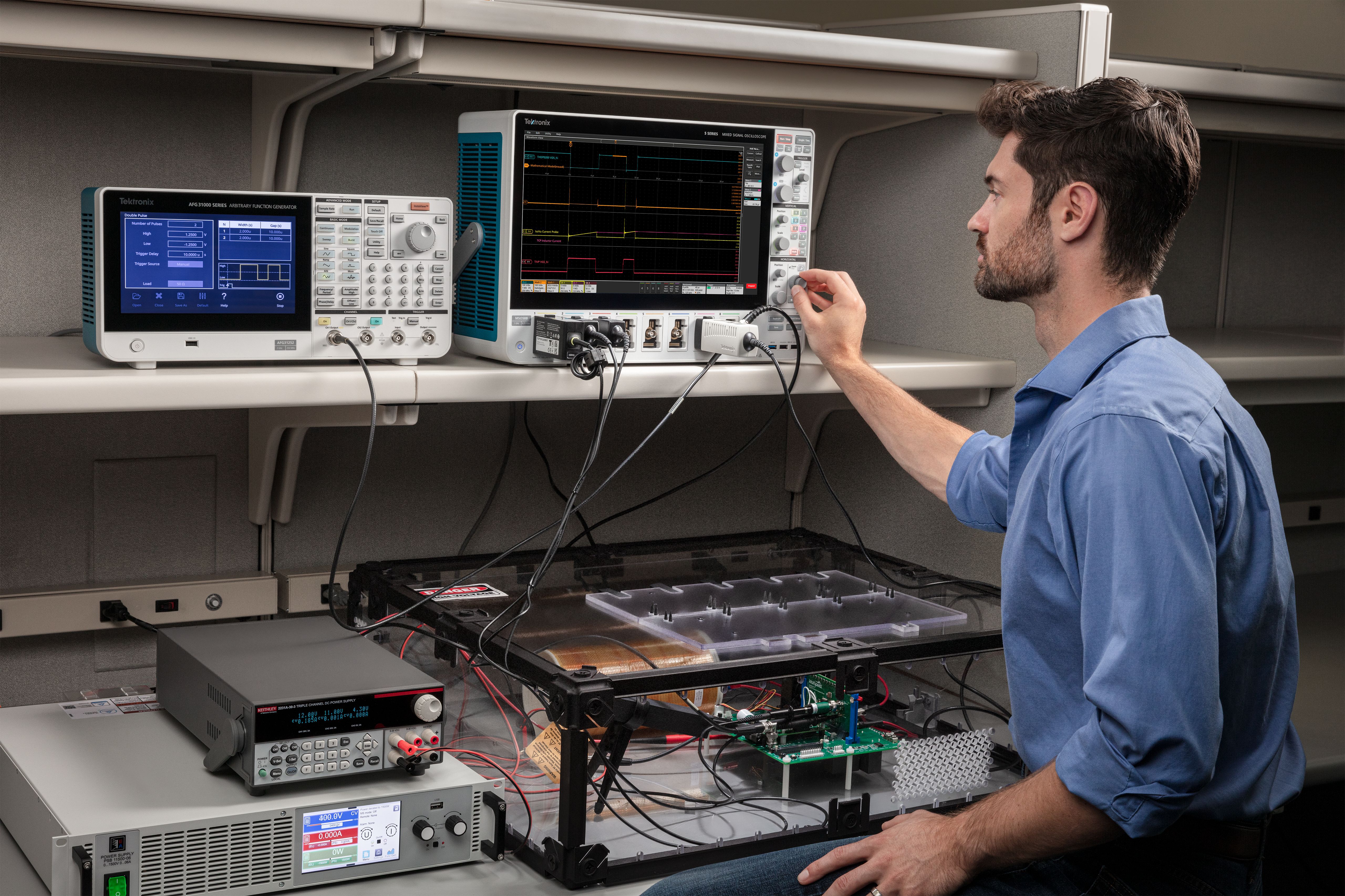
- The oscilloscope must be equipped with appropriate probes. Probe selection is critical for getting valid results and will be covered in the next section.
- Double pulse testing application software on the oscilloscope facilitates making repeatable measurements. This application note describes testing using Double Pulse Test Software Opt. WBG- DPT for 4, 5 and 6 Series B MSOs.
Double Pulse Test Software on the 4/5/6 Series MSO
The measurements associated with double pulse testing can be performed using the built-in capabilities of the 4, 5 and 6 Series MSO oscilloscopes, since these oscilloscopes include the multiplication, differentiation and integration functions as well as adjustable gating and reference levels. However, the Wide Bandgap Double Pulse Test (WBG-DPT) application (Figure 14) which is available for these instruments automates double pulse measurements without the need for any custom programming. Automated measurements can offer greater repeatability and faster results compared to manual setups and measurements.
This application note covers the math behind the measurements, but the automated DPT tools will be used in the measurement examples.
Especially when compared to manual test methods or custom code, the on-scope software provides:
- Repeatable measurements, even on signals with ringing
- Measurements per JEDEC and IEC standards or using custom parameters
- Ability to generate double pulse gate drive signal from an AFG31000 Series Arbitrary/Function Generator
- A preset feature to facilitate oscilloscope setup
- A unique deskew capability that can be performed postacquisition, without special fixtures
- Easy navigation between pulses and annotation
- Summarized measurements in results tables
- Pass/Fail testing with configurable limits and actions to be taken on failures
- Reports, session files and waveforms to help document results
- Full programmatic interface for test automation In addition to switching loss, timing and reverse recovery, the WBG-DPT application also supports automated:
- Deadtime measurements
- Dynamic RDS(on) measurements, without external clamping
These parameters can be measured using a setup similar to double pulse testing, but different probes and connections will be required.
For more information about the WBG-DPT app, please refer to the Option 4-WBG-DPT, 5-WBG-DPT, 6-WBG-DPT Application Datasheet.
Gate Drive Signal Source
DPT requires a gate drive signal source capable of providing multiple pulses with independently adjustable widths. Pulses may be generated by using a microcontroller board with custom software, but off-the-shelf signal generators can generally provide predictable performance and finer control of pulse parameters. Arbitrary/function generators (AFGs) are a cost-effective category of signal sources for this application. This can be a standalone generator or can be built into the oscilloscope. For example:
- AFG31000 Series Arbitrary/Function Generators offer a Double Pulse Test Application on the unit to quickly generate pulses with varying pulse widths. The next section gives a description of this feature. The AFG31000 Series is available with dual outputs and can serve as general-purpose function generators, independent of an oscilloscope. In this application note the AFG 31000 is controlled from its front panel, however the AFG31000 can also be connected via LAN and controlled from within the WBG-DPT Double Pulse Testing application software on the 4, 5 or 6 Series MSOs. The configuration menu for contolling a LANconnected AFG is shown in Figure 15.
- 4, 5 and 6 Series MSO oscilloscopes offer an optional built-in AFG. This AFG has many of the same capabilities of a standalone generator, but is tightly integrated into the oscilloscope, sharing the same user interface. The built-in AFG cannot be controlled by the DPT application software, but may be controlled with custom software running on Windows on the 5 or 6 Series MSO (see Double Pulse Testing Power Semiconductor Devices with a 5 or 6 Series MSO with Built-in Arbitrary Function Generator).
Generating Double Pulse Gate Signals on the AFG31000
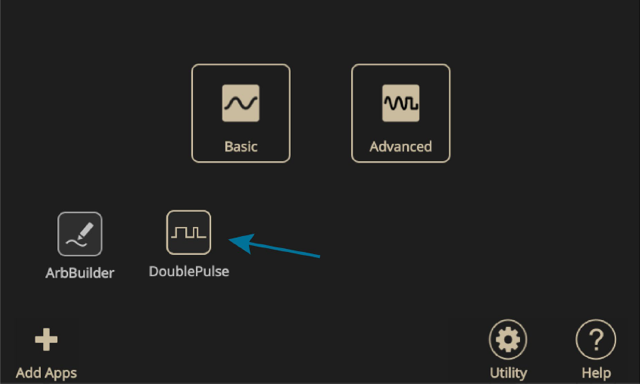
The AFG31000 Double Pulse Test Application can be downloaded directly from the tek.com website and installed onto the AFG31000. Figure 16 shows the Double Pulse Test icon on the home screen of the AFG31000 after the application is downloaded and installed on the unit.
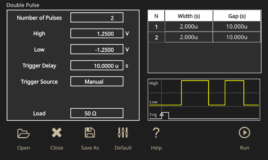
The Double Pulse Test Application lets the user create multiple pulses with varying pulse widths from the front panel of the generator. The application is intuitive and quick to set up. The first pulse width is adjusted to get the desired switching current value. The second pulse width can be adjusted independently and is usually shorter to limit heating in the DUT. The time between the pulses is also configurable.
Figure 17 shows the Double Pulse Test application window. Here the user can set the:
- Number of pulses: 2 to 30 pulses
- High and low voltage magnitude (V)
- Trigger delay (s)
- Trigger source – manual, external, or timer
- Load – 50 Ω or high Z
Oscilloscope Probing for Double Pulse Testing
The reliability of double pulse measurements depends on the choice of appropriate voltage and current probes, as well as adherence to best practices. A comprehensive discussion of probing is outside the scope of this application note, but some high-level considerations for probing in double pulse tests are included here.
First and foremost, probes and accessories must always have sufficient ratings to handle the maximum voltage or current expected in testing. This is especially true in power converter measurements since current and voltage levels tend to be higher than general electronics applications. Also, extra thought and planning must be dedicated to grounding, insulation and isolation to avoid damage or injury.
Voltage Probes
Single-ended, passive voltage probes are simpler and less expensive than differential probes, but their application in power converters is limited. This is because their reference leads are tied to earth ground through the oscilloscope. When using passive probes keep ground leads short and shield connections if possible. MMCX connectors, for example, offer high bandwidth and shielding.
Differential voltage probes are more versatile in power applications, since they are not directly connected to earth ground. They are designed for making floating measurements. Differential probes with appropriate voltage ratings are commonly used for measuring drain-tosource voltages.
Note that traditional differential probes face limitations in common mode rejection. This can impact high-side gate measurements (VGS) in which a relatively small voltage is “riding on” a high common mode signal. When making high-side VGS measurements, an isolated voltage probe is recommended as they greatly reduce common mode noise in measurements.
Current Probes
Clamp-on AC/DC oscilloscope current probes incorporate Hall effect sensors as well as coils, and are often used for measuring power converter circuits. Passive current transformers (CTs) may also be used for measurements but cannot measure DC. High-quality AC/DC probes and AC-only CTs roll off at around 100 MHz, and it is important to note their insertion inductance. This inductance, which is inherent in coil-based designs will impact the circuit under test, especially those with fast rise-time signals that occur in SiC and GaN FETs.
Rogowski current clamps are convenient for their flexibility and wide current ranges. However, they are not able to measure DC and bandwidth limitations in tens of megahertz make them of limited use in DPT.
To achieve the high bandwidth and low insertion inductance required for double pulse testing wide bandgap devices, designers often turn to shunt resistors or current viewing resistors (CVRs). Unlike general-purpose differential probes, shunt probes such as the Tektronix TICP IsoVu™ Isolated Current Probe are special voltage probes designed specifically to measure low-level signals across shunt resistors.
|
Model |
Type |
Side |
Max Current |
Bandwidth |
Rise-time |
Notes |
|
TCP0030A |
Clamp-on AC/DC |
LS, HS |
50A (peak) 30 A (rms) |
120 MHz |
<2.92 ns |
|
|
Coaxial Shunt |
CVR |
LS, HS |
100+ Amps |
2000 MHz |
0.18 ns |
|
|
Current Monitor |
CT |
LS |
100 A (peak) 2.5 A (rms) |
200 MHz |
2 ns |
|
|
Current Monitor |
CT |
LS |
5 kA (peak) 50 A (rms) |
20 MHz |
20 ns |
|
|
Current Transformer |
CT |
LS |
10 kA (peak) 35 A (rms) |
50 MHz |
7 ns |
|
|
CWT |
Rogowski Coil |
LS |
300 A (peak) |
15 MHz |
25 ns |
Probe Connections
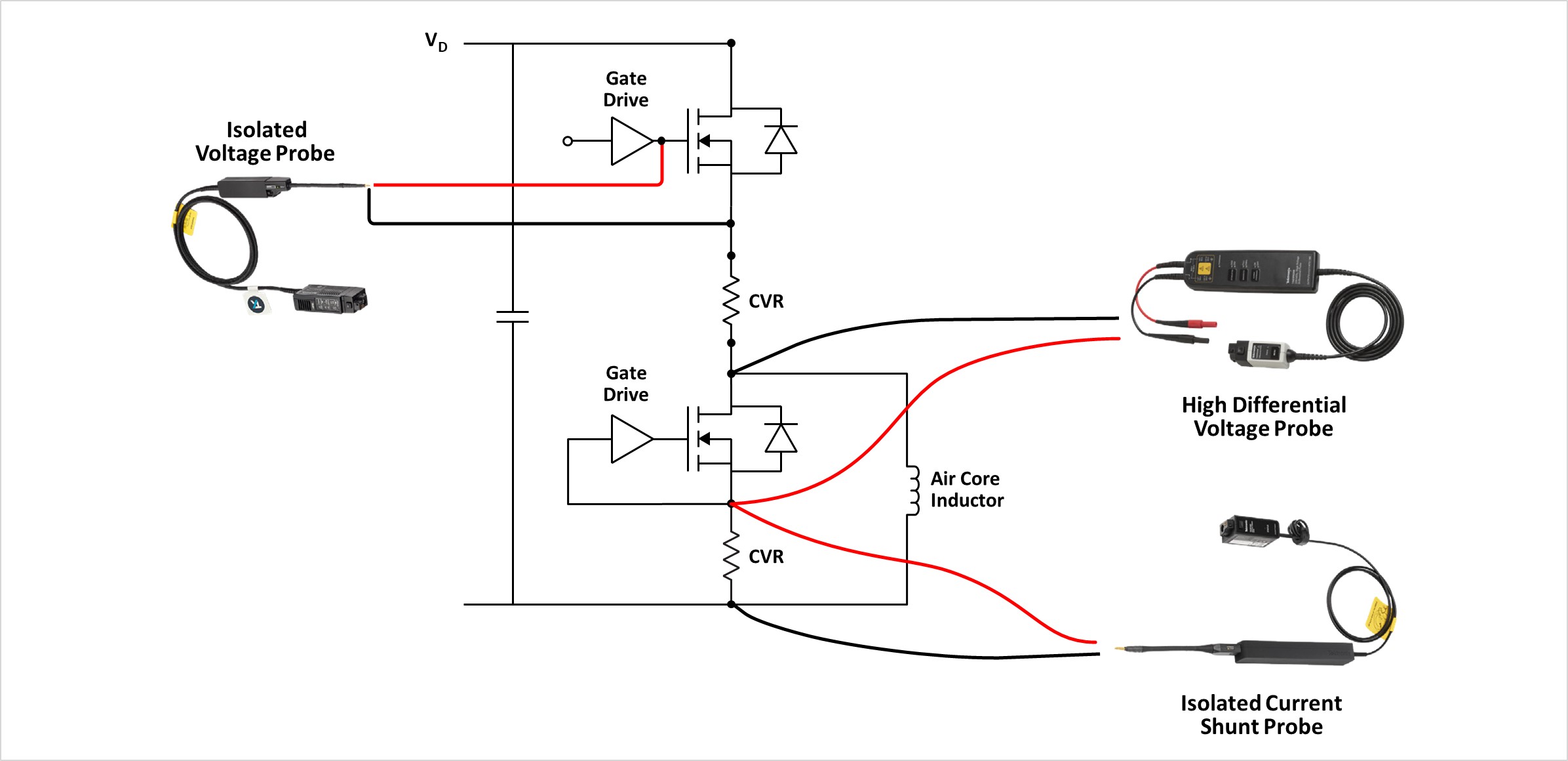
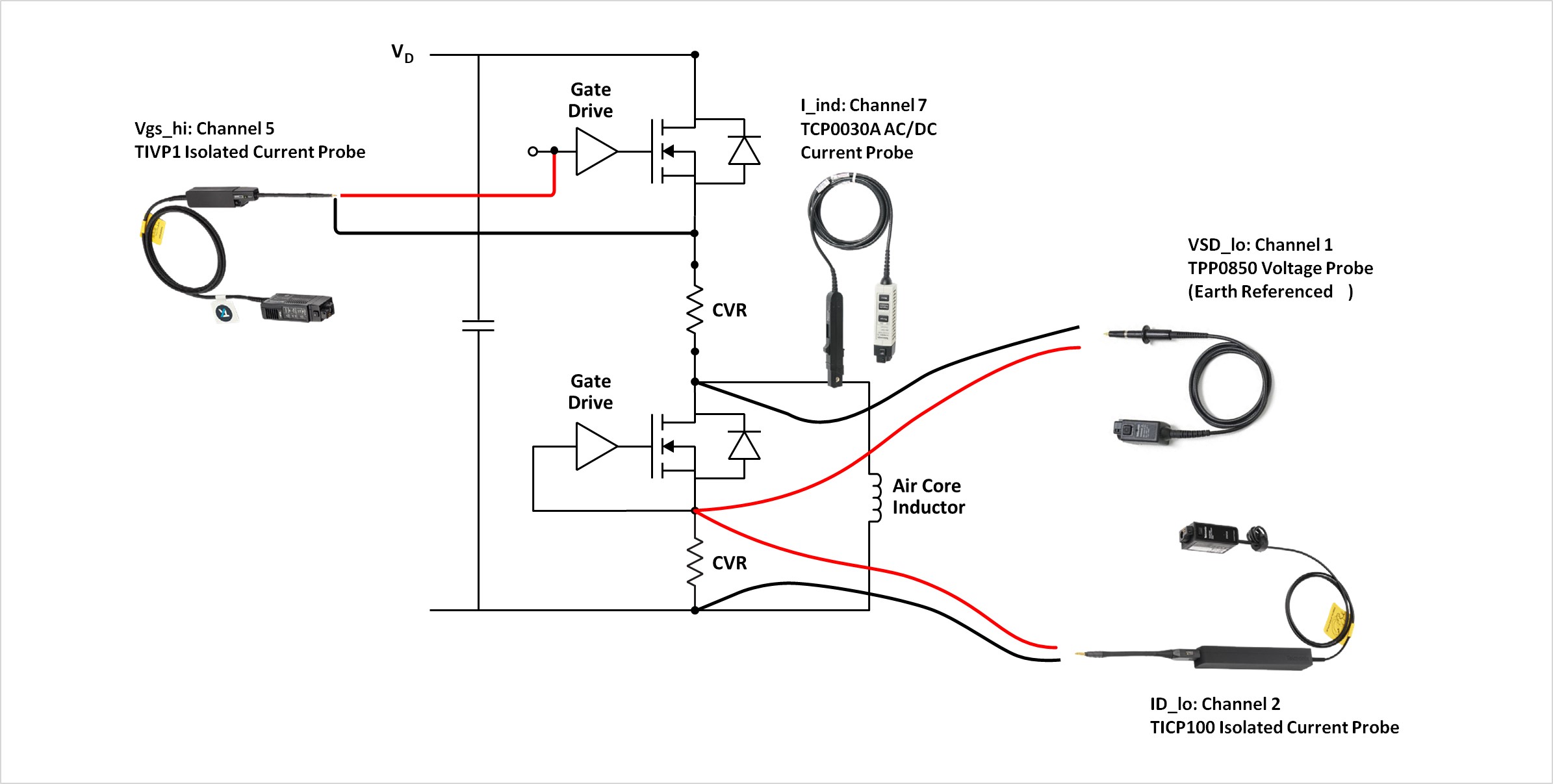
This section covers probe recommendations and connections for switching measurements. A common DPT approach is to measure switching loss on the low-side switch. Although some designers carefully drive both the high and low switches during testing, it is a common simplification to force the high-side switch off by shorting the gate to source. This is shown in Figure 18.
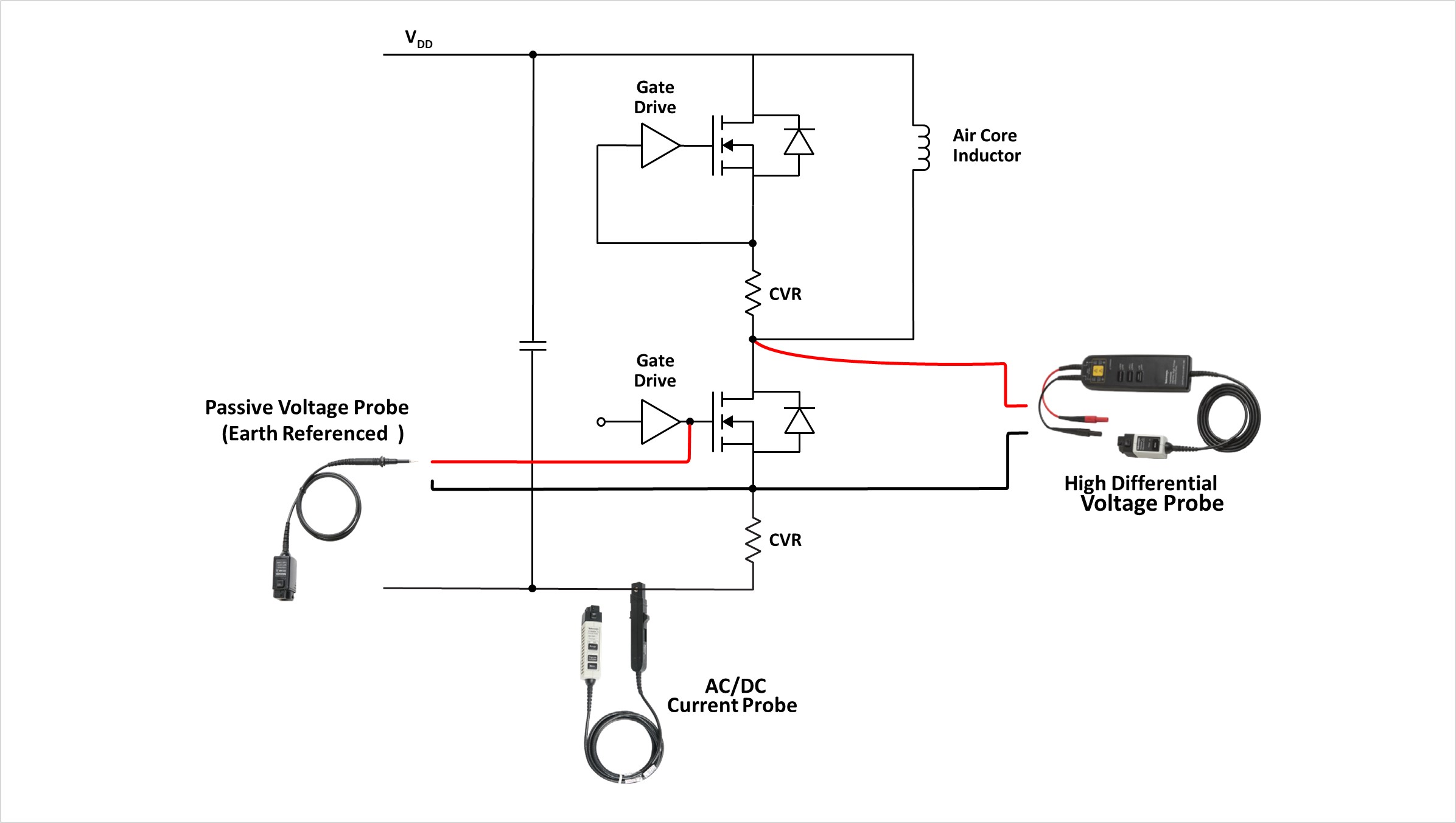
For low-side device switching testing shown in Figure 18, these probes represent a good starting configuration for most applications.
- VGS-Lo - TPP Series 10X passive probes offer an effective solution and are included with 4, 5 and 6 Series MSOs. In this case the source of the FET will be grounded through the oscilloscope. Installing an MMCX connector across the gate makes a high-bandwidth test point and optional MMCX cartridges are available for TPP1000 probes.
- VDS-Lo – High voltage passive probes are a good solution if the low-side source node can be grounded. The TPP0850 is a 50X attenuating probe rated for 1000 VRMS CAT II applications. If the source node must not be grounded, a THDP/TMDP Series differential voltage probe is recommended.
- ID-Lo - TCP Series current probe. If insertion inductance is a concern and bandwidth higher than 120 MHz is needed, then a TICP Series IsoVu Isolated Current Probe is recommended along with a high-performance shunt resistor or CVR.
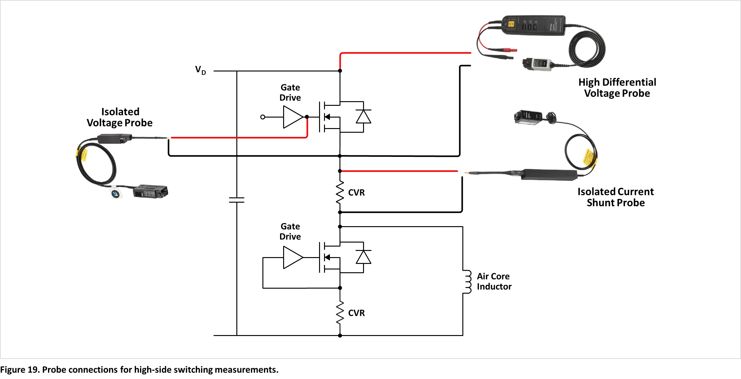
For testing switching loss on a high-side FET, as shown in Figure 19, the low-side FET is forced off, and the high-side FET is driven. These probes represent a good starting point for making measurements:
- VGS-Hi - TIVP IsoVu Isolated Voltage Probe
- VDS-Hi - THDP/TMDP Series differential voltage probe
- ID-Hi - TICP Series IsoVu Isolated Current Probe is recommended along with a high-performance shunt resistor or CVR.
An example probe configuration for testing reverse recovery of a low-side diode is shown in Figure 20. The probes in this example are:
- VGS-Hi - TIVP IsoVu Isolated Voltage Probe
- VSD-Lo - THDP/TMDP Series differential voltage probe. In Figure 20 the probe is connected across the body diode in the forward direction.
- ID-Lo - TICP Series IsoVu Isolated Current Probe is recommended along with a high-performance shunt resistor or CVR. A clamp on current probe such as a TCP Series may also be used if access is available.
Double Pulse Test Measurement Example
In this section actual measurements will be configured, taken and explained. Using an example setup, switching loss and timing will be measured on the low-side switch, and the test circuit with be reconfigured to measure reverse recovery loss on the low-side diode. Testing of the SiC FETs will be performed at 400 VDC.
The Example Test Setup
For this case study, measurements are taken on a Wolfspeed SpeedVal Kit™ Half-Bridge Motherboard with SpeedVal Kit TOLL Power Daughter Card [13]. The daughter card includes two 650 V SiC MOSFETs in a half-bridge configuration. The setup uses 1 mH air core load, and the source of the low-side FET is tied to earth ground through a shunt resistor. The test setup is shown, configured for lowside switching measurements, in Figure 21.
Instrumentation used in the examples includes:
- Tektronix AFG31252 arbitrary/function generator with Double Pulse Testing Application
- Elektro-Automatik PSB 11500-06 1.5 kW DC power supply to provide VDD
- Keithley 2231A-30-3 triple-output DC power supply (3 A at 30 V max) to power gate drivers and other low-voltage electronics
- Tektronix 5 Series B MSO oscilloscope (4 or 6 Series B
MSOs may also be used) with WBG-DPT Double Pulse
Testing application software and the following probes:
- TPP1000 300 V, 1 GHz ground-referenced probe for low-side VGS
- TIVP1 2.5 kV, 1 GHz IsoVu isolated voltage probe for high-side VGS
- TPP0850 1000 V, 800 MHz high voltage ground-referenced probe for low-side VDS measurements
- TMDP0200 750 V, 200 MHz high voltage differential probe for high-side VDS measurements
- TICP0100 1 GHz IsoVu isolated current probe for measuring drain current via shunts
- TCP0030A 30 A, 120 MHz clamp-on current probe for load inductor current
Configuring the Gate Drive Signal
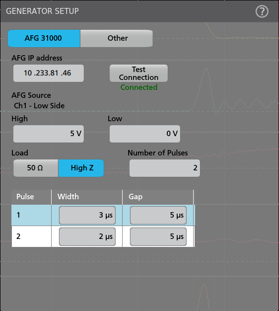
The double pulse stimulus was set on the AFG31000 as shown in the screen capture in Figure 22.
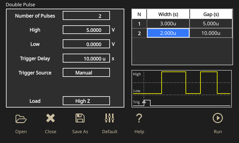
The amplitude of the pulses was set to 5 V into high impedance. The pulse width for the first pulse was set to 3 μs, the gap was set to 5 μs and the second pulse was set to 2 μs. The trigger was set to manual.
Probe Configuration for Low-Side Switching Measurements
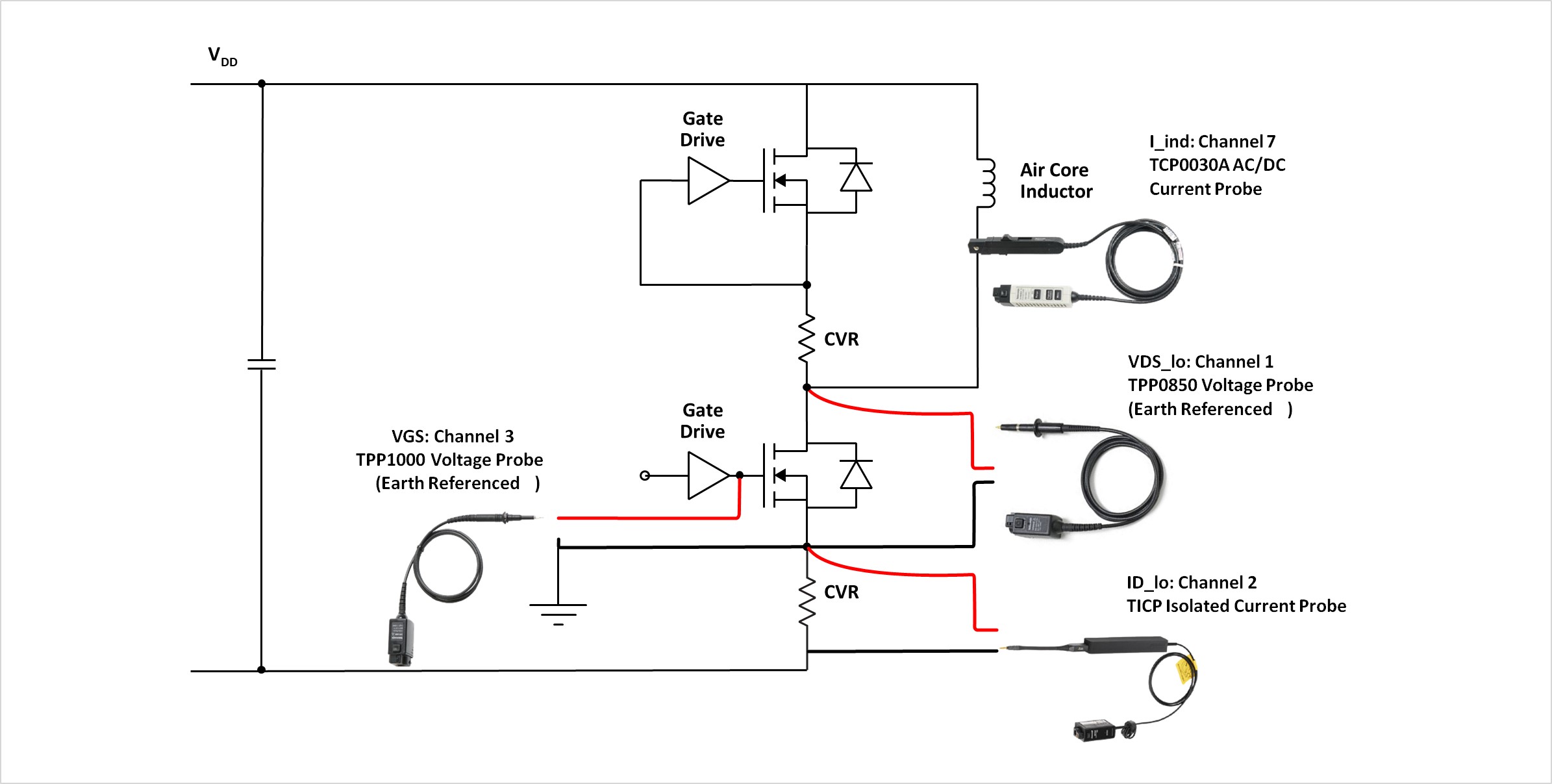
Before making any connections, always double-check to make sure circuits are de-energized!The first measurements taken were low-side switching measurements. For these measurements, the oscilloscope probes were connected as shown in Figure 23. In addition, the signal from the AFG was routed into Channel 4 for triggering.
Deskewing Voltage and Current Signals
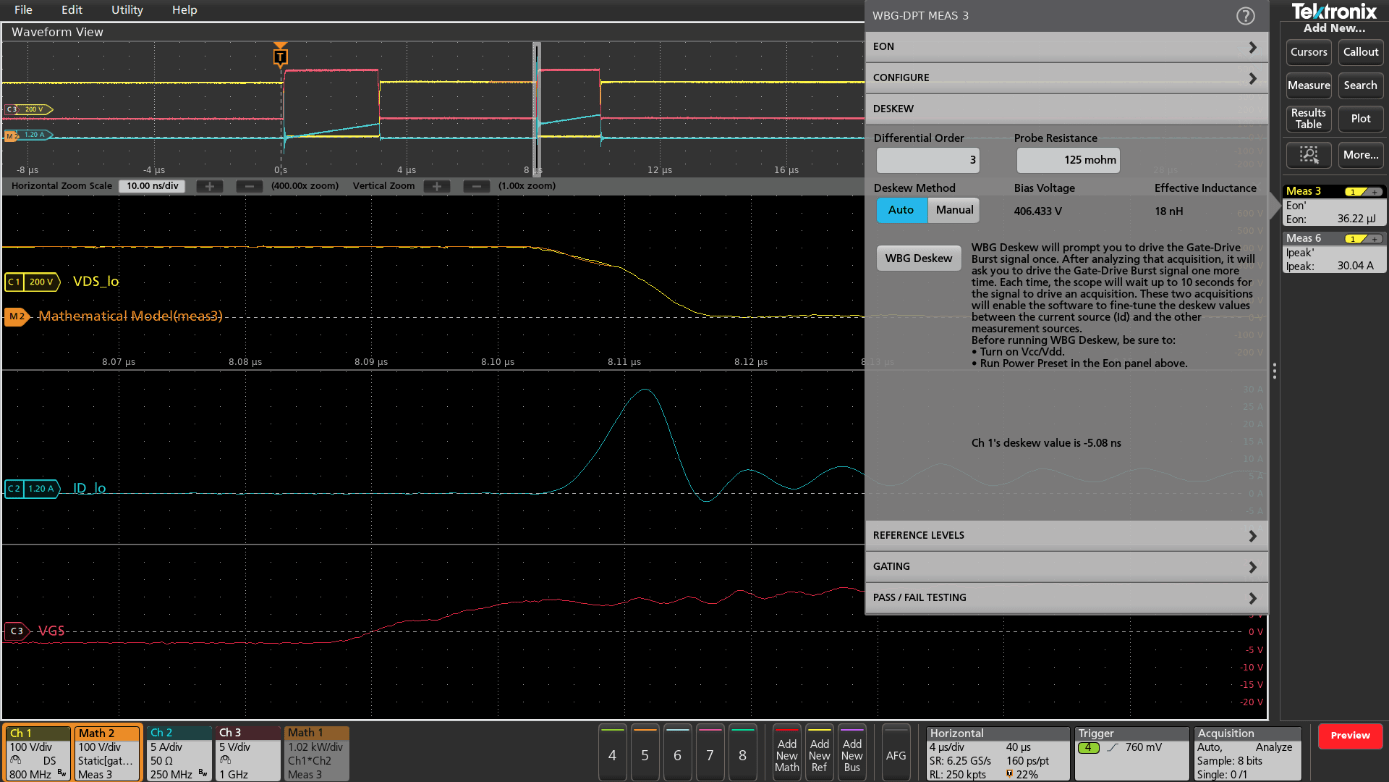
For accurate power measurements, it is critical to correct for the different delays in current and voltage probes, especially between VDS and ID. Any delays between the probes will introduce error in any power and energy measurements. In a traditional test procedure, one must perform deskew of the voltage and current probes before connecting to the DUT. However, this approach can be difficult in high-power setups, since this approach requires the use of special fixtures and/or replacing the load inductor with a resistive load.
However, in the WBG-DPT application software, the skew of the measurement system is performed as a postacquisition operation and does not require any special fixtures or signal sources [12]. The WBG Deskew function built into the WBG-DPT application software (Figure 24) calculates and corrects for the skew between VDS and ID or VCE and IC when the power device is a MOSFET or an IGBT respectively. The skew value is then applied to the VDS or VCE signal to align it with the drain or emitter current.
For the measurements that follow, the probes were deskewed by following this procedure.
Measuring Low-Side Switching Timing and Energy Losses
Switching timing measurements can be made using cursors, but care must be taken to position the cursors precisely and assign them to the correct channels, since industry standard measurements are made between edges on VGS and VDS (see Figure 8.) In this example, measurements will be defined by the WBG-DPT application on the oscilloscope to facilitate the assignment of channels and setting reference levels.
Similarly, energy losses during switching can be determined using channel math to multiply voltage and current to generate a power waveform, and using an area measurement (integration) to determine energy. To simplify this, the WBG-DPT app provides Eon and Eoff measurements under the Switching Parameter Analysis group. This measurement performs the necessary math and quickly displays the result.
Making Switching Loss Measurements with the WBG-DPT Application
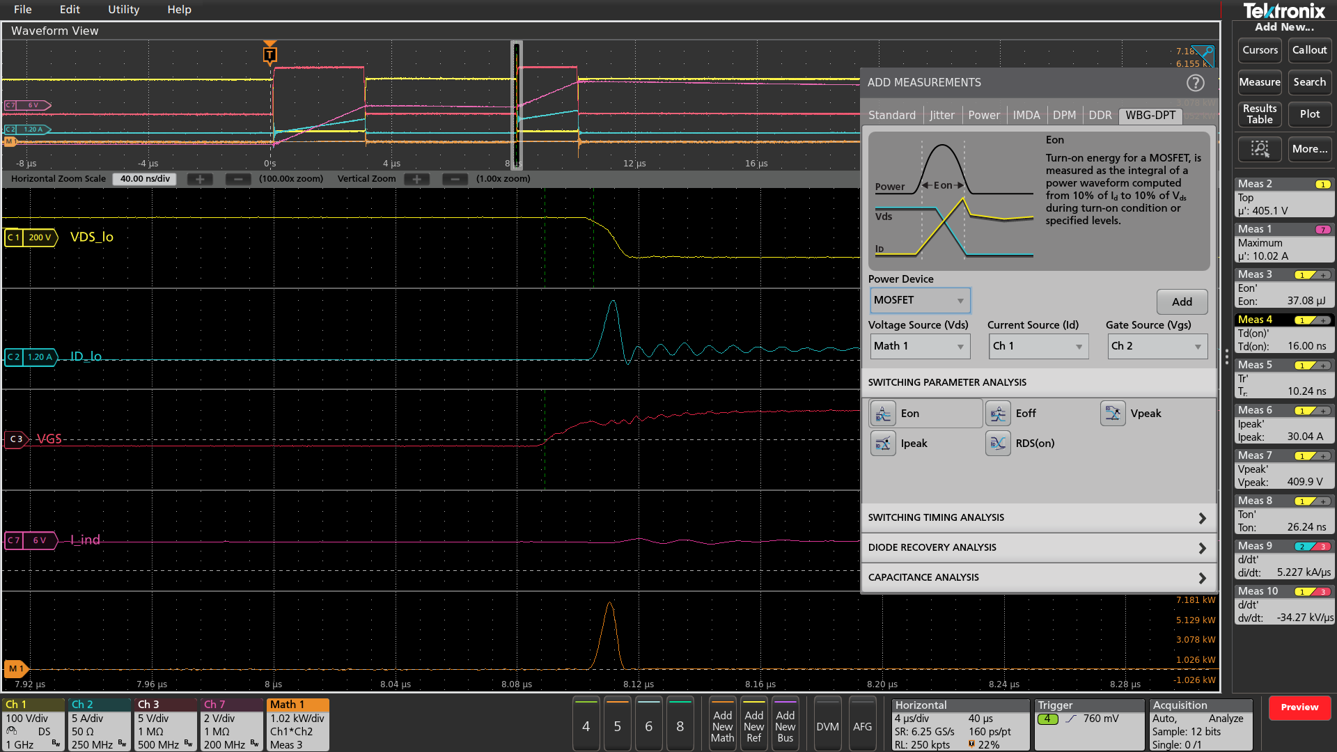
As with all measurements on the 4, 5 and 6 Series MSOs, the WBG-DPT application controls are accessed through the Measure button in the upper right corner of the touchscreen. For this example, the Power Device type was set to MOSFET. The VDS, ID, and VGS sources were set to Channels 1, 2 and 3 as shown in Figure 25.
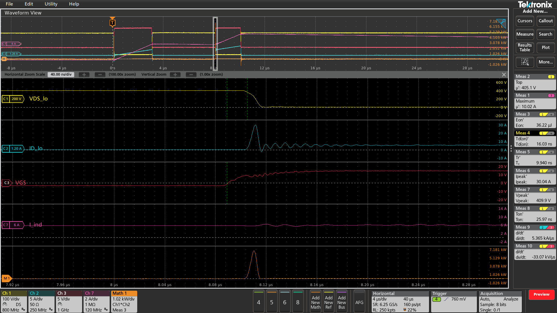
Measuring Turn-off Parameters
To measure turn-off characteristics several measurements were selected:
- “Top” amplitude measurement on VDS for monitoring
- Maximum current through the inductor for monitoring
- Turn off delay, Td(off)
- Fall time, Tf
- Peak VDS, Vpeak
- Turn-off time, Toff
- Current slew rate, d/dt
- Voltage slew rate, d/dt
- Output charge, Qoss
Each measurement can be individually configured as shown in the example for the turn-off energy measurement (Eoff) shown Figures 26 and 27.
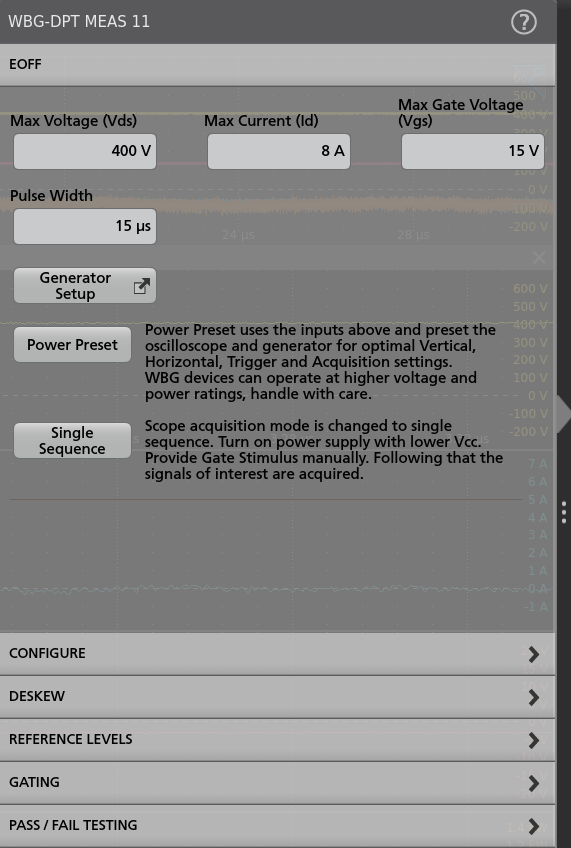
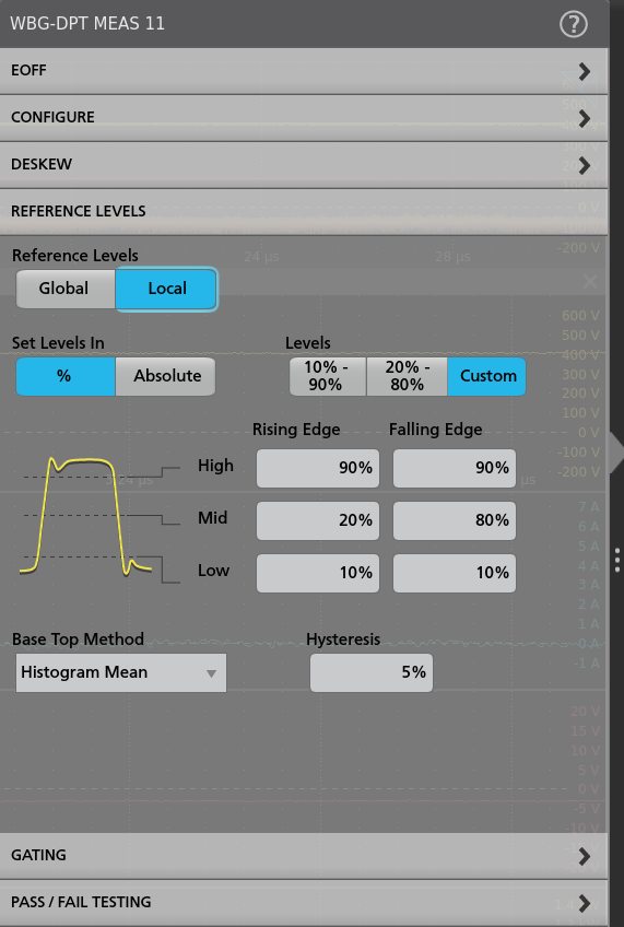
The WBG-DPT application software defaults to the industry standard 10% and 90% threshold values shown in Figure 27. It also supports custom threshold settings. The default levels are used in this example.
After double-checking connections and power supply settings, and sealing the safety enclosure, power-up of the system was started.
- First, power was applied to the gate drive electronics by activating the lower-voltage power supply.
- Power was applied to VDD by activating the high-voltage power supply. At this point the circuit high voltage was present!
- The oscilloscope was armed for an acquisition.
- The AFG31000 was triggered to generate the gate drive pulses.
- The high-voltage supply for VDD was turned off
- The low-voltage supply for gate drivers was put in standby
The resulting waveforms were captured and measurements were displayed on the oscilloscope. Data and settings were stored as a “session” to document the measurements. The screen capture in Figure 28 shows the detail of the turn-off event at the end of the first VGS pulse, after ID has risen to the target value.
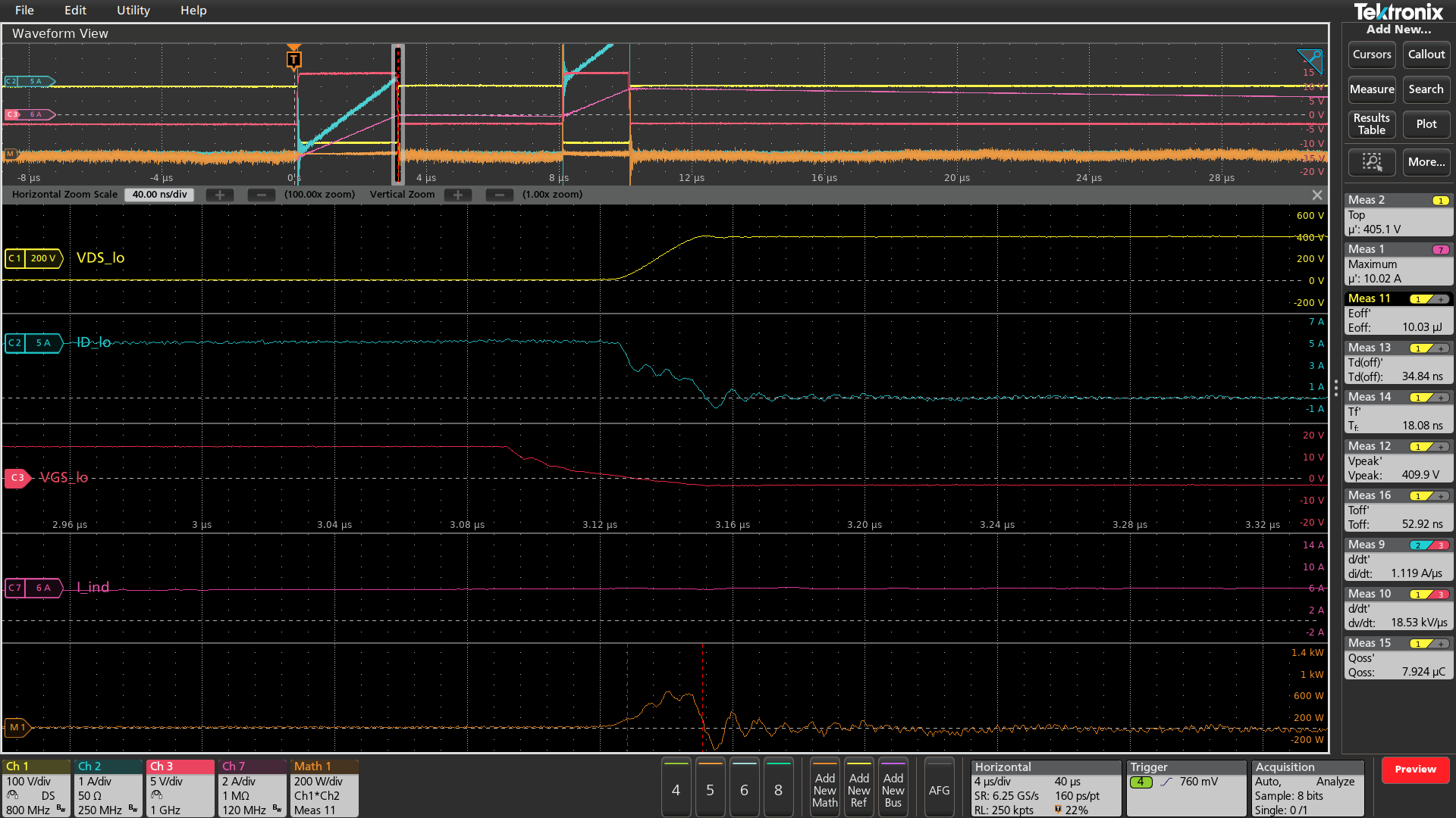
A second set of measurements were configured to document turn-on. Figure 29 shows the detail of the turn-on event at the beginning of the second VGS pulse.
Measuring Reverse Recovery
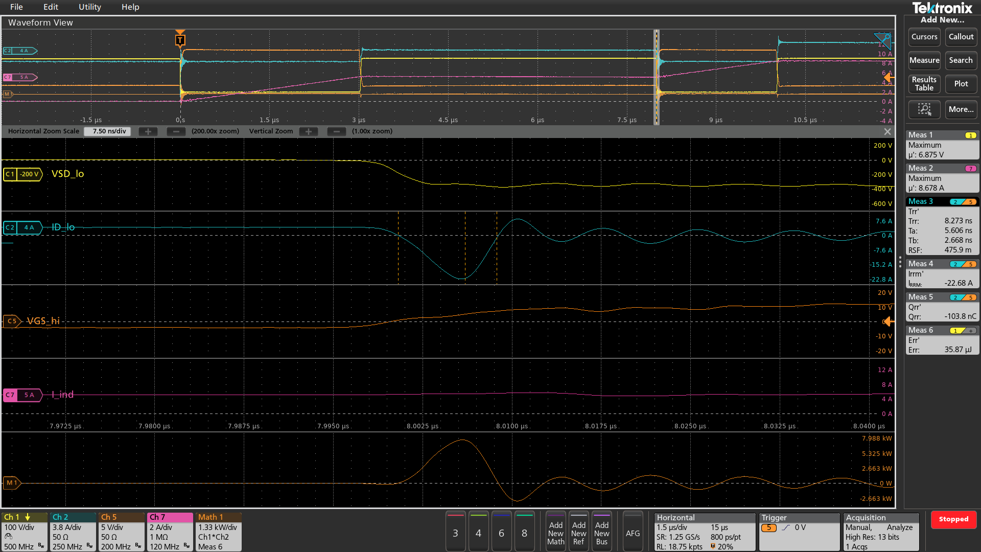
The reverse recovery characteristics of the free-wheeling diodes can be measured on the low-side or high-side devices. For this example, the diode on the low-side was measured, since the device under test provides easy access to a shunt on the low-side source, through a shielded, high-bandwidth MMCX connector. To measure the low-side diode, the load inductor must be placed across the low-side switch, and the high-side FET is pulsed. The low-side diode behaves as s free-wheeling diode, conducting inductor current when the high-side FET is turned off. Reverse recovery current will flow briefly when the high-side FET turns back on, and the low-side diode is reverse-biased.
The following measurements, found in the WBG-DPT application in the Diode Reverse Recovery group, were set up for this test:
- Peak VDS
- Maximum inductor current
- Reverse recovery time, Trr
- Minimum reverse recovery current, Irrm
- Reverse recovery charge, Qrr
- Reverse recovery energy, Err
Probe connections are shown in Figure 30. Note that the voltage probe on Channel 1 is connected in the forward direction across the low-side diode (VSD instead of VDS). The waveforms and captured measurements are shown in Figure 31.
The WBG-DPT application also allows multiple Trr measurements to be taken over more than one pulse. These measurements can be displayed in an overlapped plot to observe changes in trr over multiple pulses.
Conclusion
Double pulse testing is the preferred method for measuring switching parameters of power devices under a controlled junction temperature. This application note has covered the application of instrumentation, probes and application software to achieve high-quality, repeatable results.
Tektronix offers a wide range of instruments, probes and software to address double pulse testing applications.
Elektro-Automatik and Keithley power supplies provide precise, reliable power without taking up unnecessary space.
The AFG31000 with its Double Pulse Test application is quick and easy to set up, allowing engineers to focus on gathering data.
The WBG-DPT double pulse application on the 4, 5 or 6 Series B MSO is fully-integrated into the oscilloscope measurement system and automates testing with a wide range of measurements, the ability to control an arbitrary function generator, and innovative deskew approach. tests to analyze power devices’ behavior while saving time compared to manual testing. It defaults to industrystandard measurements but can be customized as well.
Lastly, a range of oscilloscope probes, such as low-noise isolated voltage and current probes deliver high-fidelity signals to the oscilloscope.
As explained in this application note, these elements can be combined to greatly reduce test times and achieve faster time to market for designers of next generation power converters.
References
- https://www.tek.com/document/technical-brief/evolving-materials-and-testing-emerginggenerations-power-electronics
- https://www.tek.com/document/application-note/measuring-power-supply-switching-loss-oscilloscope
- “Test Method for Continuous-Switching Evaluation of Gallium Nitride Power Conversion Devices”, JEDEC Standard JEP182, Version 1.0, January 2021
- Infineon: Double Pulse Test for IGBT & FWD – Principle https://u.dianyuan.com/upload/space/2011/07/29/1311925659-501009.pdf
- https://training.ti.com/understanding-mosfetdatasheets-switching-parameters
- https://www.mouser.com/datasheet/2/389/stfh10n60m2-974335.pdf
- https://www.st.com/resource/en/data_brief/eval6498l.pdf
- https://www.tek.com/datasheet/advanced-powermeasurement-and-analysis
- https://www.tek.com/document/application-note/measuring-vgs-wide-bandgap-semiconductors
- https://www.tek.com/en/how-to/double-pulse-testing- --energy-loss-measurements
- https://www.tek.com/en/products/referencesolutions/ wide-bandgap-double-pulse
- https://www.tek.com/en/blog/a-new-softwaredeskew- approach-accelerates-double-pulse-testing
- https://www.wolfspeed.com/products/power/ evaluation-kits/speedval-kit-modular-evaluationplatform/