Oscilloscopes
Application Notes
Solution Briefs
Probe Selection Guide
3/11/2025Videos
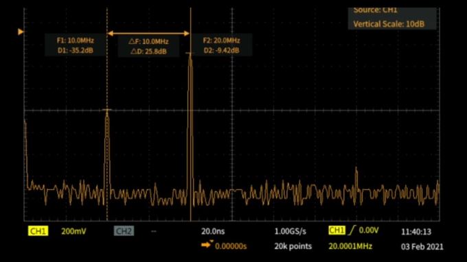
What is Fast Fourier Transform
4/2/2021Webinars
Case Studies
Download
Download Manuals, Datasheets, Software and more:
Contact us
Call us at
Available 6:00 AM – 5:00 PM (PST) Business Days