Introduction
Manufacturers of transistor devices tend to start their design prototype evaluations to yield characteristic information, while still working in their research and design labs. While straight DC testing is the norm in most cases, some of these devices are expected to be operated with a pulsed or brieflyon (switched) stimulus to yield a certain behavior or outcome. The test setups may seem simple on the surface but learning and understanding how to use the instrumentation involved in said tests can often require a steep learning curve. Even after learning to physically operate the equipment, generating the code to automate the testing process can also come with its own challenges as well as a time investment. Ideally, there would be some sort of existing software that can intuitively simplify as much of the testing and automation process as possible.
This document will first introduce the reasons why pulsebased testing might be beneficial for a semiconductor device. Further details are supplied that specifically indicate the application of pulsed test for MOSFET transistors. Additionally, specifics are provided to help guide the reader in using the Keithley KickStart Software to establish automated tests for these devices and generate both tabular and graphical representations of their data.
Benefits of Pulse Testing
The most common reason for using pulsed measurements is to reduce joule heating (i.e., device self-heating). When a test signal is applied to a device under test (DUT), the device consumes power and turns it into heat, increasing the device’s temperature. The longer that power is applied, the hotter the device becomes, which affects its electrical characteristics. If a DUT’s temperature can’t be kept constant, it can’t be characterized accurately. However, with pulsed testing, power is only applied to the DUT briefly, minimizing self-heating. Duty cycles of one percent or less are recommended to reduce the average power dissipated by the device over time. Pulsed measurements are designed to minimize the power applied to the device so much that its internal temperature rise is nearly zero, so heating will have little or no effect on the measurements
Because they minimize joule heating, pulsed measurements are widely used in nanotechnology research, where it is necessary to characterize delicate materials and structures like CNT FETs, semiconductor nanowires, graphene-based devices, molecular-based electronics, and MEMs structures. The heat produced with traditional DC measurement techniques could easily alter or destroy them.
To survive high levels of continuous DC power, devices like MOSFETs and IGBTs require packaging with a solid metal backing and even heat-sinking. However, during the early stages of device development, packaging these experimental devices would be much too costly and time consuming, so early testing is performed at the wafer level. Because pulsed testing minimizes the power applied to a device, it allows for complete characterization of these devices on the probe station, reducing the cost of test.
The reduction in joule heating that pulsed testing allows also simplifies the process of characterizing devices at varying temperatures.
Semiconductor devices are typically so small that it is impossible to measure their temperature directly with a probe. With pulsed measurements, however, the selfheating of the device can be made so insignificant that its internal temperature can be assumed to be equal to the surrounding ambient temperature. To characterize the device at a specific temperature, simply change the surrounding ambient temperature with a thermal chamber or temperaturecontrolled heat sink. Once the device has reached thermal equilibrium at the new ambient temperature, repeat the pulsed measurements to characterize the device at the new temperature.
Pulsed measurements are also useful for extending instruments’ operating boundaries. A growing number of power semiconductor devices are capable of operating at 100 A or higher but building an instrument capable of sourcing this much DC current would be prohibitive. However, when delivering pulse mode power, these high-power outputs are only needed for very short intervals, which can be done by storing the required energy from a smaller power supply within capacitors and delivering it all in one short burst. This allows instruments like a high-power source measure unit (SMU) to source high current (or voltage) levels with precision current and voltage measurements.
Measuring I-V Curves of a MOSFET
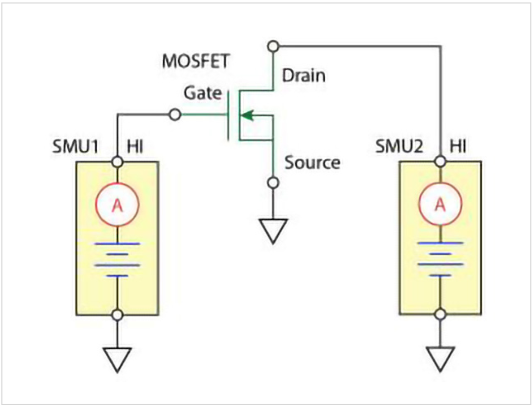
Semiconductor devices (e.g., transistors) are the foundation of electronic products. Most devices need to be electrically characterized in various settings of the research and development process: research labs, fabs, universities, device manufacturers, etc. Keithley is the industry leader in I-V characterization of transistors. Using SMU instruments for semiconductor characterization is ideal because of their ability to both source and measure, especially low currents. Testing devices that have more than two terminals usually requires more than one SMU.
However, a two-channel SMU can perform most characterizations on a single field effect transistor (FET).
Figure 1 shows two SMUs in use for I-V characterization of a MOSFET.
Examples of common measurements made in I-V characterization of transistors are as follows:
- Drain Voltage (VD) - The voltage appearing at the drain terminal of a FET is called the drain voltage.
- Drain Current (ID) - The current taken from the voltage source by the drain terminal is called the drain current. Drain current can yield a lot of insight on the device’s operation and efficiency.
Other common measurements include:
- Gate Voltage (VG)
- Gate Current (IG)
- Threshold Voltage (VTH)
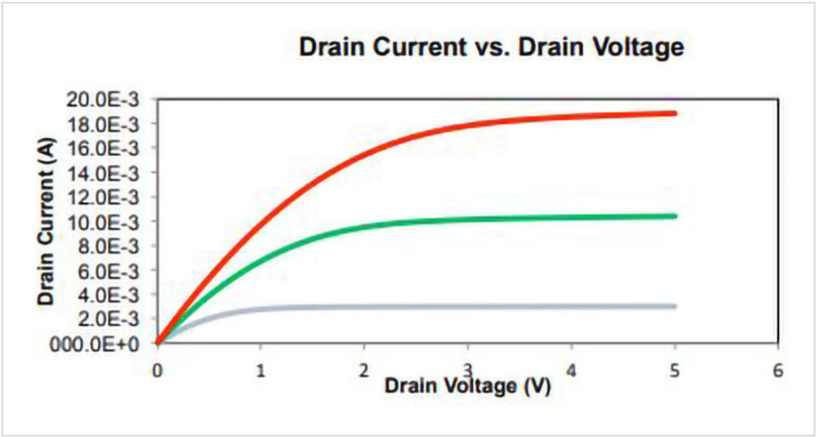
Figure 2 shows a MOSFET drain family of curves generated by using a dual-channel Keithley SourceMeter® SMU instrument.
Pulsed I-V characterization (as alluded to previously, wherein voltages and currents are applied for a very short time and at a limited duty cycle) is another common way to measure I-V curves and can be accomplished using the KickStart Software. Pulsed I-V measurements can reduce test times and allow for MOSFET characterization without exceeding its safe operating area or causing the device to self-heat and its parameters to shift.
Two pulsed I-V channels are typically used to measure these MOSFET I-V curves with one channel connected to the gate and the other to the drain. The ground of each channel is connected to the MOSFET source pin.
To construct the transistor curves, the gate channel first applies voltage to the gate, then the drain channel sweeps VDS through a range of values, measuring the resulting current at each point. Next, the gate channel applies a different voltage to the gate and the process repeats, constructing the next MOSFET I-V curve in the set.
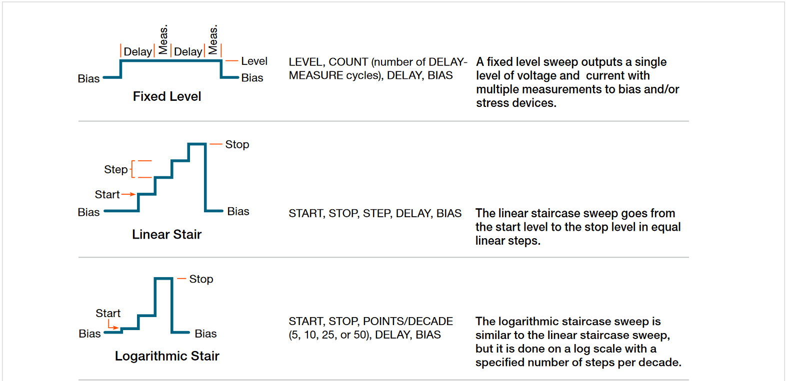
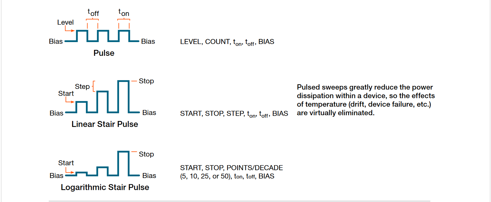
A SMU can simplify this process with built-in pulsed and DC sweeps, including linear staircase, logarithmic staircase, and custom sweeps (Figure 3). All sweep configurations can be programmed for single-event or continuous operation.

Measuring Pulsed I-V Characteristics of FETs in KickStart
This example application demonstrates how to use a Series 2636B SMU instrument to perform pulsed I-V characterization of FETs. The 2636B is a good choice for semiconductor device testing because it can quickly and accurately source and measure both current and voltage.
Determining the I-V parameters of FETs helps you ensure that they function properly in their intended applications, and that they meet specifications. There are many I-V tests that you can perform with the 2636B, including gate leakage, breakdown voltage, threshold voltage, transfer characteristics, and drain current. The number of 2636B instruments required for testing depends on the number of FET terminals that must be biased and measured.
This application shows you how to perform a drain family of curves (Vds-Id) on a three-terminal MOSFET. The MOSFET is the most commonly used FET because it is the basis for digital integrated circuits.
Equipment and Software Required
- One 2636B SourceMeter SMU Instrument
- Keithley KickStart Startup Software version 2.6.0 or later, installed on your computer; you can download the KickStart software from tek.com/keithley-kickstart.
- Four triaxial cables (Keithley 7078-TRX-10)
- A metal-shielded test fixture or probe station with female triaxial connectors
- A triaxial tee connector (Keithley 237-TRX-T)
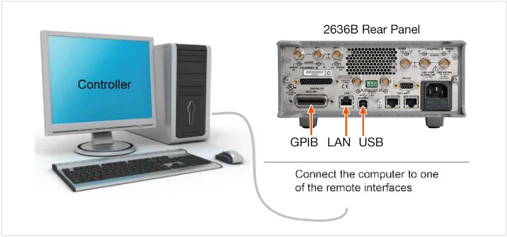
- Use one GPIB cable, one USB cable, or one ethernet cable
Set up Remote Connections
This application is configured to run remotely. You can run this application from any of the supported communication interfaces for the instrument (GPIB, USB, or ethernet).
Figure 4 shows the rear-panel connection locations for the remote communication interfaces.
To perform a drain family of curves, configure both instruments to source voltage and measure current.
In this circuit, you connect the Force HI terminal of 2636B SMUB to the gate of the MOSFET and connect the Force HI terminal of 2636B SMUA to the drain.
You connect the source terminal of the MOSFET to the Force LO terminals of both 2636B channels. You need a second 2636B (or a 2635B single channel SMU) if you want to source and measure from all three terminals.
Figure 5 shows an I-V test configuration for a MOSFET using the two 2636B instrument channels.
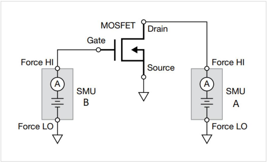
Figure 6 shows the connections from the rear-panel terminals of the 2636B channels to the MOSFET.
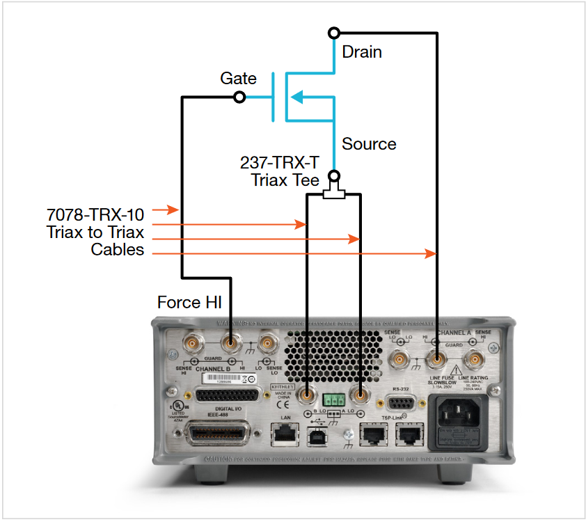
For this application, connect four triaxial cables (7078-TRX10) from the 2636B rear-panel female triaxial connectors to the MOSFET device. Mount the MOSFET device in a metalshielded test fixture with female triaxial connectors. Connect the Force LO terminals of both 2636B channels to the Source terminal of the MOSFET using a triaxial tee connector (237-TRX-T).
Launch KickStart and Set Up the Test
Once the communication cable is connected between the computer and the 2636B, you are ready to launch the KickStart software.
To create the test project:
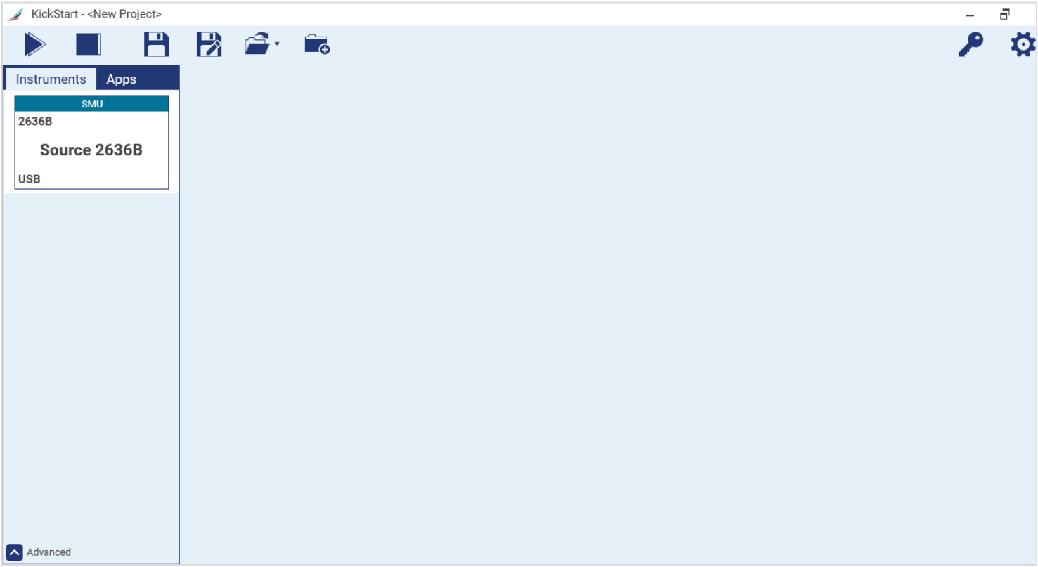
- Launch the KickStart software. The startup screen is displayed, as shown in Figure 7.
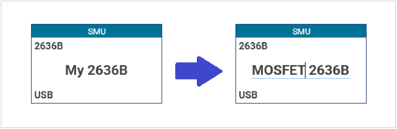
- In the instrument instance, click on the centered label to rename to “MOSFET 2636B”. Note that this is not a mandatory step but a means to show how you might apply customized names to your instruments in the event that you have several SMUs or other instruments to choose from in the KickStart user interface.
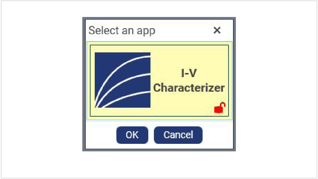
- Either double-click or drag the MOSFET 2636B instrument into the main app staging area then select I-V Characterizer.
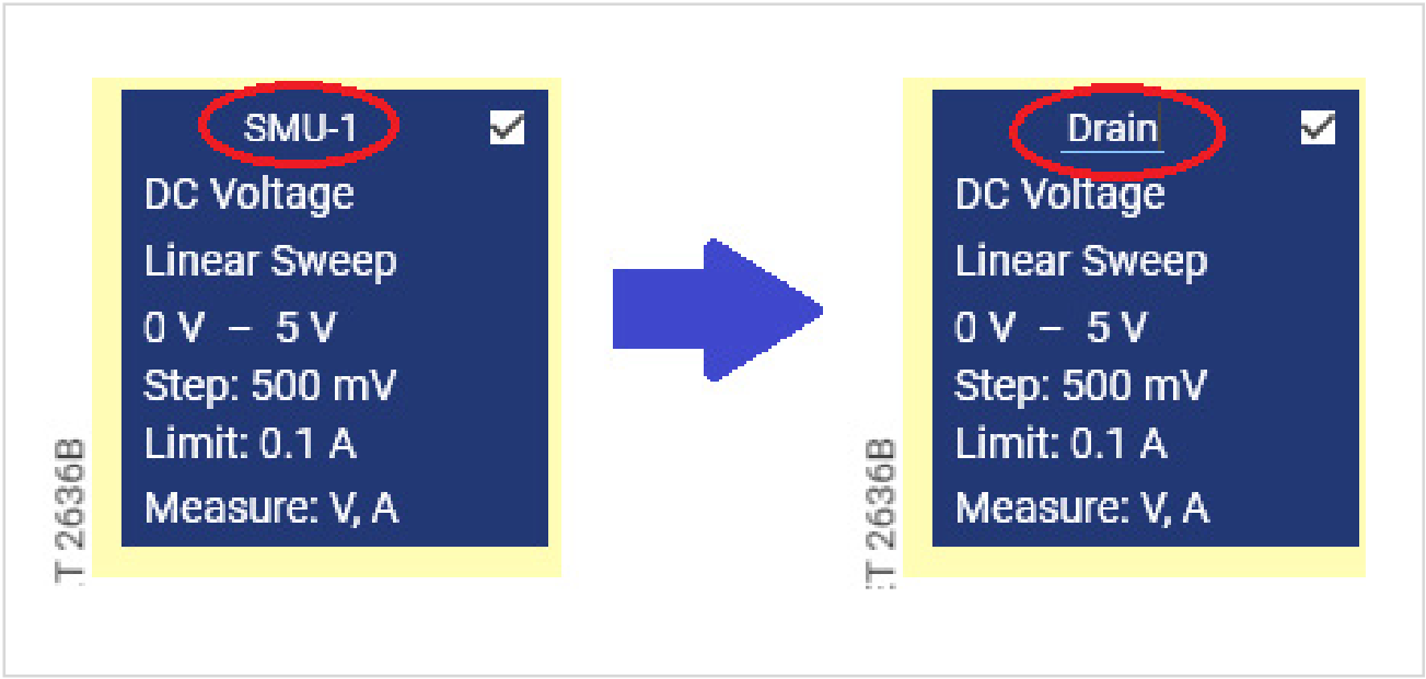
- Navigate to the SMU-1 channel settings tab and modify the channel label to read “Drain”.
- Apply the following drain source changes (illustrated in Figure 11):
- Set the Type to Pulse.
- Set the Function to Voltage.
- Set the Mode to Sweep.
- Set the Start level to 0 V.
- Set the Stop level to 10 V.
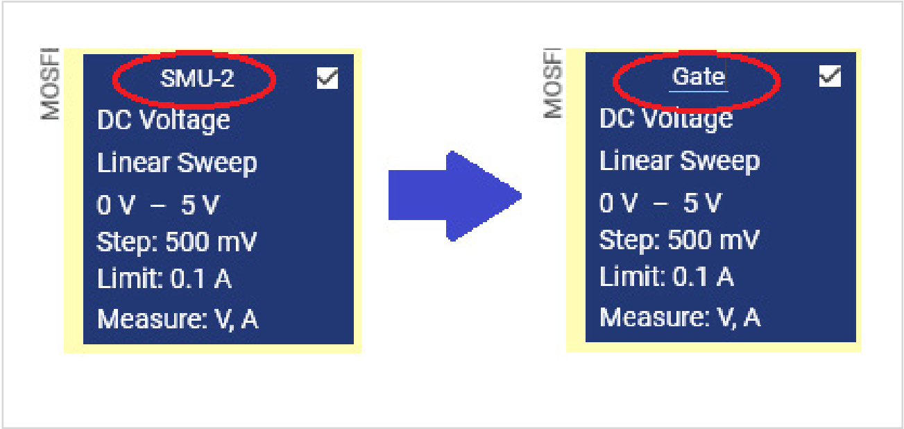
- Navigate to the SMU-2 settings tab and modify the channel label to read “Gate”.
- Apply the following Gate source changes (illustrated in Figure 13):
- Set the Type to Pulse.
- Set the Function to Voltage.
- Set the Mode to Sweep.
- Set the Start level to 3 V.
- Set the Stop level to 5 V.
- Set the Limit to 10 mA.
- In the Measure settings area, change the Range to 10 mA.
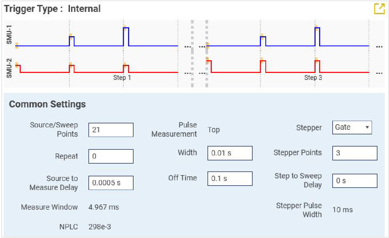
- Navigate to the Common Settings pane and apply the following settings:
- Set the Source/Sweep Points to 21.
- Set the Source to Measure Delay to 5e-4 s.
- Set the Width to 10 ms.
- Set the Off Time to 100 ms.
- Set the Stepper to Gate.
- Set the Stepper Points to 3.
- Note, too, how the Waveform Viewer pane updates to show the output of each SMU channel, with the Gate stepper (SMU-2) applying a set level for each of its defined steps and the Drain sweeper (SMU-1) performing a sweep at each of the gate step levels.
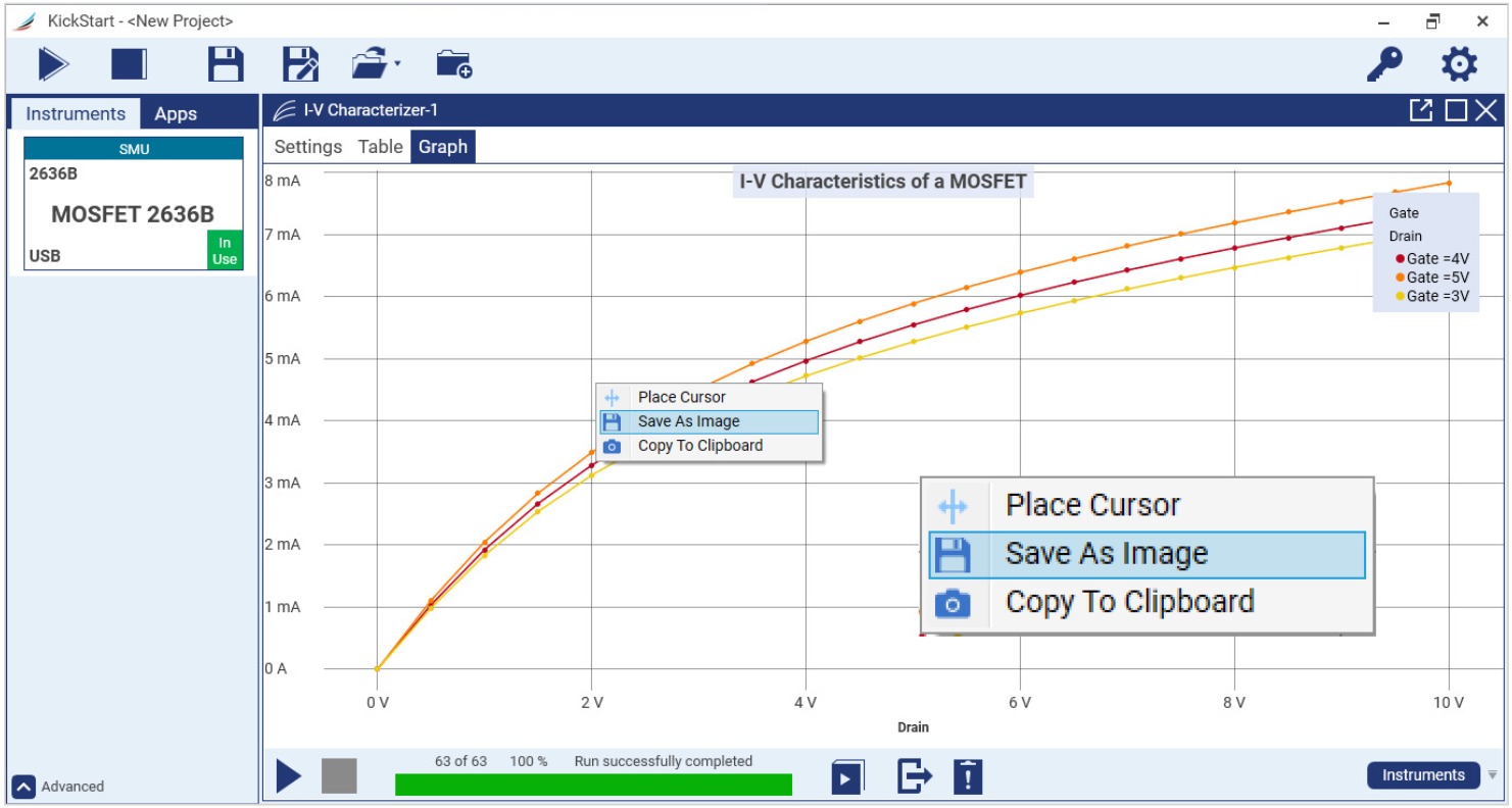
- Click on the Run button to execute the test.
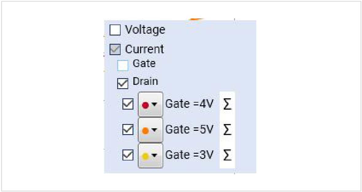
- Click on the Graph tab at the top of the KickStart user interface.
- Hover your mouse cursor above the legend and deselect the Current data for the Gate.
- Hover your mouse cursor in the top center area of the graph to reveal the title entry field and provide a title of your choosing to your graph.
- You have immediate visualization of your data but also have the option to save the graph image as a *.png file or copy to the clipboard for immediate pasting into messages or reports.


Summary
The primary reason for pulse testing is to reduce device self-heating that happens when the device is activated – especially at its maximum operating potential – for increasing periods of time. Early device designs where proper packaging or heat sinking are not yet in place are the perfect stage at which to employ pulse testing. For IGBTs and power MOSFETs this can help yield early insights into device performance, potentially leading to flaw detection and design modifications.
Whatever your pulse-based testing needs, Keithley source measure units and KickStart software are an ideal pairing to help quickly establish your test setups, collect data, and share tabular and graphical insights with your colleagues. The KickStart examples shared within this document use the Series 2636B SMU that are capable of achieving 10 A, 50 W in its pulse operating region. However, keep in mind that KickStart also supports the 2651A (for higher current up to 50 A) and 2657A (for higher voltages up to 3000 V) SMUs.