Contact us
Call us at
Available 6:00 AM – 5:00 PM (PST) Business Days
Download
Download Manuals, Datasheets, Software and more:
Feedback

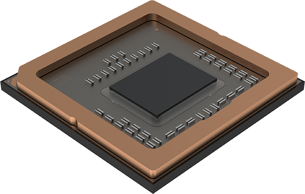
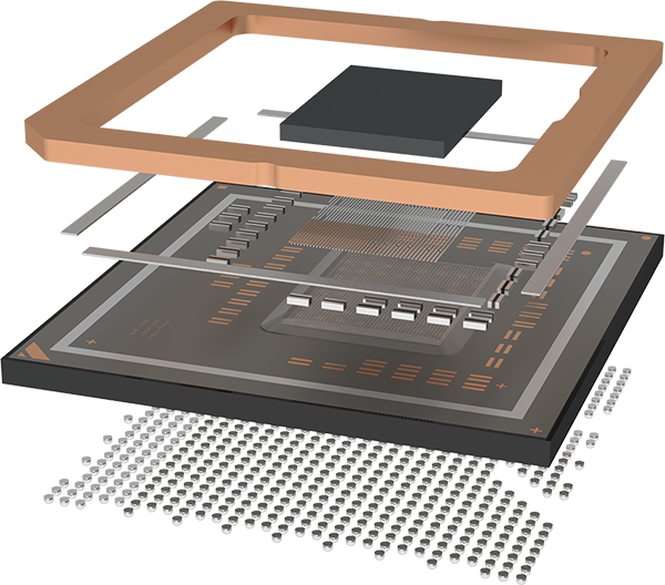
Advanced Package Assembly and Test Services
With more than 60,000 square feet of Class 10,000 (ISO 7) and Class 1k (ISO 6) clean-room space, Tektronix Component Solutions' domestic manufacturing facility is suited for prototyping and manufacturing at all scales. We support a variety of IC assembly and hybrid technologies, including wire bonding, flip chip ball grid arrays (FCBGA), multi-chip modules, and various other configurations. Our flexible manufacturing space and diverse base of IC packaging and hybrid technologies helps make us an ideal partner for building high-performance, high-complexity devices for mission-critical defense and industrial applications.
For projects requiring wafer processing (e.g., wafer bumping, thinning, dicing), we maintain relationships with a variety of domestic and international industry suppliers and offer supply chain management capabilities to enable a turnkey solution for your microelectronic parts.
Die Attach and Package Sealing Capabilities
The Tektronix Component Solutions technical team has successfully completed hundreds of interposer and package designs for a wide range of ASIC packages; from large, high density flip-chip ASICs (13,000 interconnects) to high speed flip chip MCMs (35GHz). Flip-chip assembly is performed in-house with qualified assembly processes for bump pitches down to 148 microns. Tektronix flip-chip assembly expertise also includes proven material sets for ultra-low-K dielectric ASICs and assembly experience with a variety of semiconductor foundries and process nodes.
For basic die attach requirements, Tektronix Component Solutions utilizes solder or epoxy bonding methodologies. For more advanced requirements, such as hermetic packaging, Tektronix Component Solutions can employ eutectic die attach techniques. Additionally, we offer flip chip assembly and wire bonding services for a wide variety of package configurations. Our package sealing capabilities include traditional epoxy and seam seal with electroless or electrolytic plating for hermetic devices.
As packaging requirements expand beyond traditional wire-bonding and flip-chip, Tektronix Component Solutions is developing state-of-the-art packaging and test techniques for 2.5D and 3D packaging architectures.
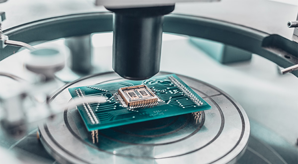
Package Test
Since our inception, IC package test has been an integral part of the support we provide Tektronix and our capabilities in this area remain a core competency that leverages experienced personnel and capable equipment. From wafer test to in-line and final test, we have the IC package test solutions to verify components and modules are operating at required performance levels.
In the case of turn-key IC package or hybrid development projects, our test development team works closely with our designers to optimize the design of each package for testability. By designing for testability, we are better able to validate the performance of assembled devices before delivery.
We offer analog, digital, mixed-signal, and semiconductor testing services to validate the performance of a wide variety of parts. With time and frequency domain measurements from DC to > 50 GHz and swept frequency measurements up to 110 GHz, our high-speed test capabilities are ideal for parts destined for high-performance defense applications.
The test of custom, high-performance parts often goes beyond just the ability to electrically verify operation and includes additional test restrictions (e.g., zero ambient light). Our ability and willingness to develop custom test systems and fixtures to support strict test requirements sets us apart in the assembly and test services industry.
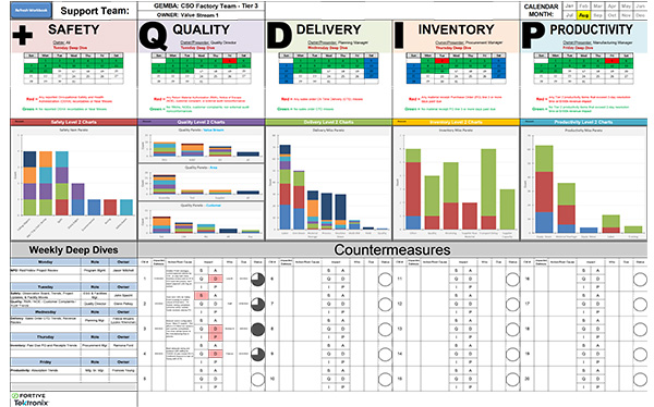
Lean Manufacturing
Tektronix Component Solutions applies lean manufacturing principles throughout our facility and is focused on continuous improvement to remove waste, streamline processes and ensure that assembly activities are providing value to our customers. To support this goal, our manufacturing lean cells are constantly evaluated on strict standards of safety, quality, delivery, inventory and productivity (+QDIP). +QDIP metrics are clearly communicated at each cell by a visual management system, allowing managers and operators to quickly assess performance at any given time. With these metrics as a guide, our manufacturing team consistently seeks to pro-actively enhance the design and flow of lean cells to improve performance (e.g. takt time, yield, throughput). This focus on continuous improvement helps to proactively reduce risk and ensure quality and consistent delivery.
As a proven US-based, ITAR-registered supplier to a variety of defense programs and companies, Tektronix Component Solutions is an ideal partner for defense applications requiring high-performance, mission-critical microelectronics. Offering services and products that include wafer test, IC packaging assembly and test, 2.5/3D packaging, and design & simulation, Tektronix Component Solutions has the expertise and capabilities to meet your requirements for high-reliability microelectronics.
With more than 40 years of experience, Tektronix Component Solutions is the stable supplier that you can trust to deliver on long-term military programs.
Trusted, ITAR-Registered Supplier
Tektronix Component Solutions has been accredited by the U.S. Department of Defense (DOD), Defense Microelectronics Agency (DMEA) as a Category 1A microelectronics Trusted Source for IC packaging/assembly and test services – the highest designation awarded by the U.S. Department of Defense. This enables Tektronix Component Solutions to serve U.S. defense customers with classified program requirements. The accreditation certifies that Tektronix Component Solutions meets stringent product control and security standards in providing trusted microelectronic services. Tektronix Component Solutions also holds certifications in ISO9001/ISO14001 and AS9100D and meets all ITAR requirements.
As an on-shore, ITAR-registered supplier, Tektronix Component Solutions has stringent standards in-place to protect and control sensitive information related to defense programs. With many years of experience supporting defense customers and programs, we recognize and adhere to the added level of responsibility in providing microelectronic engineering and manufacturing services to the military.

High-Performance Products and Services
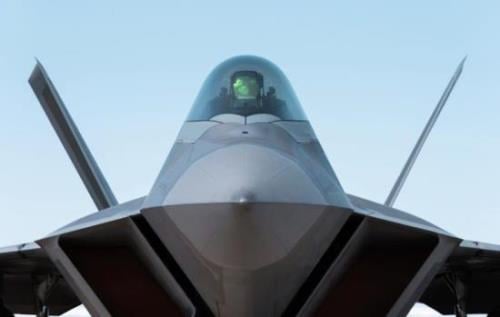
Our military experience spans a variety of critical applications, including communications, avionics, radar, propulsion control, and guidance systems. Tektronix Component Solutions has supplied high-performance and high-reliability products to defense programs such as the F-22 Raptor and F-35 Lightning II (Joint Strike Fighter) with a focus on continual C-SWaP (cost, size, weight and power) improvements.
Having served military and commercial aerospace customers for many years, Tektronix Component Solutions has a deep understanding of the high-reliability requirements of those applications. As such, we fully utilize our unique strength in test to deliver fully-tested parts that have proven to operate successfully in mission-critical environments.