Thermal management is critical when testing laser diodes at the semiconductor wafer, bar, and chip-on carrier production stages. As a result, pulsed testing is commonly used to minimize power dissipation. However, several sources of error remain when pulse testing high power laser diodes, including problems with coupling high current pulses to the DUT, optical detector coupling, and both slow response and inaccuracy in the detector itself. This paper explores solutions to each of these problems that can deliver shorter test times, more accurate results, and lower reject rates.
LIV Curves
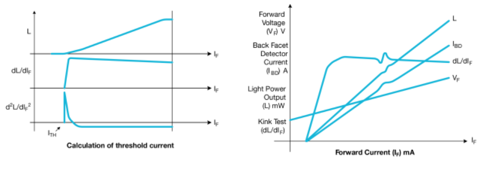
The fundamental test of a laser diode is a Light-Current-Voltage (LIV) curve, which simultaneously measures the electrical and optical output power characteristics of the device. This test is primarily used to sort laser diodes or weed out bad devices before they can be built into an assembly. The device under test (DUT) is subjected to a current sweep while the forward voltage drop is recorded for each step in the sweep. Simultaneously, instrumentation monitors the optical power output. The resulting data is then analyzed to determine laser characteristics, including lasing threshold current, quantum efficiency, and "kink" detection (localized negative slope in the first derivative optical power output vs. injection current curve).
Thermal Management and Temperature Effect
Pulsed LIV testing is best done early in production, before the laser diode is assembled into a module. For diodes still on the wafer, such as Vertical Cavity Surface-Emitting Lasers (VCSELs), or in a bar (edge emitting lasers), pulsed testing is essential because the devices have no temperature control circuitry at that point. Testing with DC would, either change their characteristics, or at worst, destroy them. Later on in production, when they've been assembled into modules with temperature controls, the devices can be DC tested and the results compared to those from the pulsed test. Some devices will pass a DC test and fail a pulsed test due to device characteristic changes resulting from temperature shift.
VCSELs can be tested at the wafer stage prior to dicing because they radiate optical power perpendicular to the wafer plane. Although many VCSELs can be tested in non-pulsed mode due to their high efficiency,higher power devices require pulsed testing in the early stages of production. This avoids high thermal gradients that would induce mechanical stresses if non-pulsed DC testing were performed.
The first opportunity to test an edge-emitting laser diode is at the bar stage, where a linear array of diodes is cut from the wafer to expose the sides where light exits. After the wafer has been cut into bars, the edges of the bar are polished to form a suitable optical interface. The individual diodes on the bar then undergo LIV testing before further processing. The data from these tests are used to correlate optical performance characteristics, electrical characteristics, and semiconductor process information.
Once a laser diode has passed the bar stage tests, it is diced into chips, which are mounted on sub carriers. These small metallic or ceramic mounts are designed to ease handling of tiny laser chips during final assembly of the laser diode modules (LDMs) in which they are used. Chip-on-carrier or chip-on sub mount testing is performed to ensure that performance characteristics have not changed during the dicing and mounting steps.
LIV characteristics are a function of laser temperature, which must be tightly controlled during the test,just as in normal operation. The principal reasons for performing low-duty-cycle pulsed LIV testing are thermal management, thermal response, and transient response. Typically, these issues arise because of the need to perform DC testing of laser diodes prior to mounting on a thermal management device, such as a heat sink or thermoelectric cooler (TEC), which is sometimes called a Peltier device.
When a laser diode is properly mounted on a TEC and operated in an LDM, its temperature can be maintained within ±0.005°C. During a typical uncooled, non-pulsed LIV test, self-heating affects the electrical and optical performance of the laser. An internal temperature shift changes the forward voltage drop, dynamic resistance, quantum efficiency, and other characteristics. With short duration pulses (typically, <1µs and <1% duty cycle), the laser diode's average power dissipation has minimal thermal effects
Nevertheless, it has been found that laser diodes with poor pulsed LIV performance may pass non-pulsed DC testing. These faulty devices often cause high bit error rates in LDMs used for fiber optic data communication systems. Another class of failures is characterized by good pulsed LIV characteristics while failing non-pulsed tests. Typically, these devices become optically unstable a few microseconds after lasing is initiated, accompanied by optical output dropping to a fraction of the expected power level.Therefore, comparing pulsed and non-pulsed LIV sweeps at appropriate production stages provides a better indication of DUT performance and the effectiveness of thermal management devices built into the LDM.
Pulse Parameters
Testing a laser diode properly requires a current pulse of the right shape. It should reach full current fairly quickly (but not so fast that it causes overshoot and ringing), then stay flat long enough to ensure that the result accurately represents the laser diode's true output.
The first challenge in a pulsed LIV test is delivering constant current pulses with suitable magnitude,duration, duty cycle, and rise and fall times. To optimize kink detection, the difference in pulse characteristics between adjacent current steps in the LIV sweep must be as deterministic as possible. Two common methods of delivering current pulses are a pulsed constant current source coupled directly to the laser diode, and the use of a pulsed constant voltage source driving a known resistance. The pulsed current source is the more deterministic of these two methods. By comparison, when applying a pulsed voltage source to a laser diode, the dynamic resistance of the laser must be considered. As current through the laser increases, the resistance decreases. When using a voltage source for an LIV sweep, compensating for this resistance shift greatly complicates delivery of known currents.
The maximum source signal amplitude for a pulsed LIV test can typically exceed the nominal operating current of the laser diode by a factor of two. For early stage testing. It is common to use pulse widths of 500ns to 1µs, with a duty cycle of about 0.1%. Currents can range from a few tens of milliamps to several amperes. These test conditions are driven by the desire to minimize the average power dissipation while keeping test duration as short as possible. This can put great demands on the system, especially with respect to impedance matching.
The rise and fall times of the high current pulses should be short enough to preserve the flat time at the top of the current pulse. The sum of the rise time and the fall time should be less than 30% of the total pulse width to allow for signal settling time and flat time at the top. On the other hand, keeping the slew rate as low as possible reduces the high frequency spectral content, which helps reduce pulse transmission problems and settling time
Pulse Delivery and Impedance Matching
Typical voltage pulse sources, as well as many current pulse sources, have a characteristic output impedance of 50Ω. This is a good "match" for a standard 50Ω coax cable, and ensures minimal signal distortion when a pulse is transmitted on such a cable that is terminated in a 50Ω impedance. However, a typical laser diode has a characteristic impedance of about 4Ω. Connecting a 50Ω coax directly to the 4Ω laser diode results in a severe impedance mismatch.
One way to reduce the mismatch is to place a resistor in series with the laser diode. The optimal resistance value is the transmission line impedance in ohms, less the laser diode characteristic impedance, or approximately 46Ω. Unfortunately, this technique has a seriously negative side effect. To overcome the added resistive load, the pulse source must generate a voltage equal to the resistance of the load times the desired current. According to Ohm's Law, the voltage needed to overcome the 50Ω load and drive five amperes is 250V. This is not only a safety hazard for personnel but a hazard to fixture and components. With this level of test voltage, imagine the results of poor electrical contact between the DUT probe and a laser chip. A 250V arc would be immediately followed by a 5A current flow. The laser diode would be unlikely to survive this event and remain useful.
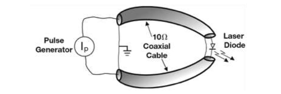
The most elegant method of avoiding this mismatch is to use a pulse source and transmission line with a characteristic impedance identical to that of the laser diode. When this is the case, the potential required to drive a 5A pulse through a 4Ω impedance is only 20V. However, the use of low impedance coax has its own problems related to changing dynamic resistance in the laser diode. There's another alternative: make the laser diode electrically part of the center conductor of a 10Ω line (Figure 2) and feed the whole thing with a pulsed current source. That way, it takes less than 10V to push 5A through the diode. And because the system has a current source, problems with changing dynamic resistance in the laser diode can be avoided.
Even the most careful impedance matching is not perfect, however, so it is a good practice to keep all transmission lines short to minimize the effect of reflections and ringing. If the drive circuit and laser diode generate reflections, the length of the transmission line strongly affects the settling time of the signal. The reason to keep the connections short is to minimize the area (and hence, the inductance) of the loop formed at the connection to the laser diode. Remember that the voltage across an inductor is given by:
| V = | L | di |
| dt |
Reaching the desired slew rate of 5A/50ns requires 10V/nH. Unless the loop area is kept very small, the required voltage can easily exceed the compliance voltage of the instrument, dramatically extending the settling time. A short cable helps reduce settling time and improves test throughput by reducing the time between reflections.
Monitoring Pulse Integrity
To ensure accurate test results, maintaining pulse integrity is essential. At first thought, it might seem reasonable to connect a scope probe across the laser diode to view the voltage signal shape and amplitude at the junction. However, this apparently simple test is fraught with potential problems. Before undertaking such a test, ask yourself: Can the oscilloscope ground be connected to the low potential lead of the laser diode without affecting the laser's pulse output? If not, can the scope ground be floated, or can the scope operate off batteries? Is the scope probe suitable for operating in the range of 500MHz to 1GHz?
All connections to a laser diode must be approached with caution. What seems to be a harmless scope probe can drastically alter electrical characteristics by appearing as the transmission line equivalent of an unshielded and unterminated conductive stub. This changes the impedance at the probe connection, results in reflections from the unterminated stub, and can lead to destructive undershoot.
Using a shunt resistor to monitor the current pulse is an acceptable technique, provided the resistance is a small fraction of the laser diode resistance, and the shunt resistor has low capacitance and inductance.A common wire wound resistor is not a good choice because it would create a high impedance path for the high frequency components of the current pulse.
Coupling to the Detector
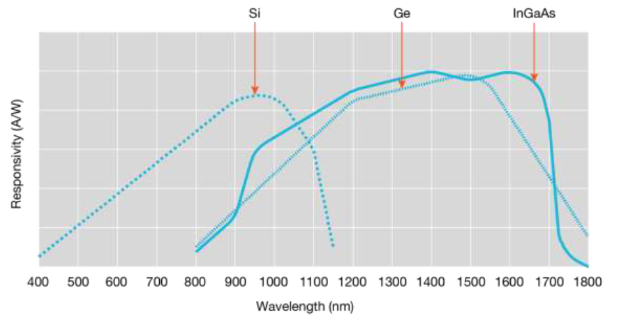
Capturing the pulsed optical output of the laser diode is not an easy task. Three detector materials are commonly used: silicon (Si), germanium (Ge), and indium gallium arsenide (InGaAs). Each has its advantages and disadvantages. As Figure 3 shows, the choice of detector depends largely on the wavelength of light involved. At wavelengths less than about 800nm, silicon is the only choice. But much telecommunications work is done between 1300nm and 1700nm, where it would appear that InGaAs would be best because its response is fairly uniform and it holds up well to about 1700nm.
The output from the laser diode can be coupled to the detector in several ways. One is simply to put the laser right against the detector, but this method has several drawbacks. Not all the light may reach the detector.
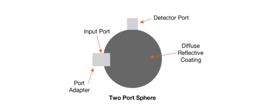
Often, the best solution is an integrating sphere a hollow ball coated on the inside with a diffuse reflecting material and equipped with a mounting for a detector and a port for feeding in the light to be measured (Figure 4). The integrating sphere accepts all the light from the source, randomizes its polarization, and distributes it evenly over its inside surface. A detector mounted through the side of the sphere then "sees" a measurable and repeatable fraction (about 1%) of the light fed into the sphere. There's plenty of light to measure but not enough to overpower the detector
Capturing Pulsed Laser Optical Output
One of the most difficult tasks in DC pulse testing is capturing the pulsed optical output of the laser diode at its peak values. The short duration optical pulse is not a friendly signal for most commercial optical power meters. Typically, optical power meters are designed for high precision measurements that often require many seconds of integration time to complete one reading. Although it is possible to use these instruments, they require long integration periods to accumulate several thousand laser pulses. Then the firmware, or an external PC-based test program, must calculate peak optical power using the assumption that average power is a function of the duty cycle for the current pulse driving the laser. A further assumption is that the integral of the noise signal is zero.
Because of optical power meter deficiencies, test engineers have also devised faster, more accurate methods for pulsed LIV testing. Measuring voltage and current in the laser diode fed with high speed pulses isn't easy. Even putting a scope probe on the diode to measure the voltage can cause problems,as explained previously. Measuring current is a little more straightforward. A low value resistor (one with a value much lower than the resistance of the laser diode) connected in series will work, but it must have low capacitance and inductance. A wire-wound resistor, which is basically a lossy inductor, is unsuitable for high frequencies.
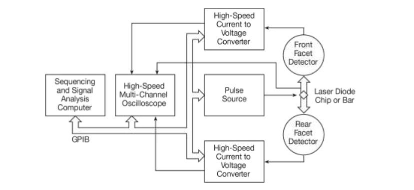
Historically, the most common method has employed a combination of rack-mounted instruments, along with fairly complex, custom-designed software running on a PC controller. In addition to the PC used for test sequencing and signal analysis, the equipment list for this system includes a pulse source, optical measurement components (photodiode detectors, etc.), a pair of high-speed voltage-to-current converters, and a high-speed multichannel Digital Sampling Oscilloscope (DSO).
The design approach to this type of system is to include both pulsed and non-pulsed operating modes.This dual functionality allows both types of LIV sweeps to be performed on a single platform, using the same measurement channels. Comparing pulsed and non-pulsed test results provides more complete information on DUT performance. Also, the dual-mode source can be located in a remote test head,which shortens the distance between the pulse source and the laser diode without having to locate the instrument physically at the laser test station. As mentioned previously, a short cable helps reduce settling time and improve test throughput by reducing the time between reflections.
System Speed and Throughput
Today, efficiency and low cost are vital to surviving manufacturing production environment. Testing must be fast, accurate and inexpensive. This means an optical power meter is a bad choice because it integrates light output over time, with a low duty cycle input that can make for an extended integration period. In addition, the accuracy of the measurement depends on how accurately the duty cycle of the pulses is known and how closely the duty cycle of the light output matches the duty cycle of the electrical input.
It has been standard practice to use a rack full of equipment (Figure 5), including a pulse source, optical measurement components (photodiode detectors, etc.), a pair of high speed current-to-voltage transimpedance amplifier (TIA) or converters, and a high speed, multi-channel DSO. The pulse source produces a pulse and the other instruments measure the electrical and optical response, feeding the results via GPIB to a PC. This process may take a few thousand pulses. This would seem to improve sensitivity, resolution, and accuracy, but it can cover up problems with waveform distortion. It is also a lengthy process, taking anywhere from tens of seconds to several minutes per DUT.
Ideal Solution and Conclusion
A more ideal solution would include all the instrumentation functionality shown in Figure 5 in a single instrument. This type of instrument would essentially be a pulsed source-measure unit with output impedance and cabling that closely matches the impedance of the laser diode. The measurement portion of the system would incorporate multi-channel data acquisition, dedicated timing circuitry, high speed current-to-voltage converters, and a digital signal processor (DSP) that emulates DSO functionality and controls much of the measurement sequence. The sequencing of the LIV sweep would be orchestrated by an internal DSP that is programmed only once for a given test sequence and can execute complete pulsed LIV sweeps without interaction with the other equipment or the control computer. The ideal instrument would also provide control signals directly to the component handling system via a digital I/O port. By incorporating all the relevant functions in one instrument, a next-generation LIV test system can greatly accelerate test throughput and lower the cost of production.
Find more valuable resources at TEK.COM
Copyright © Tektronix. All rights reserved. Tektronix products are covered by U.S. and foreign patents, issued and pending. Information in this publication supersedes that in all previously published material. Specification and price change privileges reserved. TEKTRONIX and TEK are registered trademarks of Tektronix, Inc. All other trade names referenced are the service marks, trademarks or registered trademarks of their respective companies.
0717– 1KW-61212-0