Abstract
The Fibre Channel standard is evolving to include the next generation "16G" data rate. Specifications show a line rate of 14.025 Gb/s and use of 64b/66b encoding. In this paper, we study the measurements needed to test an SFP+ transceiver to the 16G Fibre Channel standard, covering both Multi- Mode 850 nm and Single Mode 1310 nm interfaces. That is followed by a test and characterization example using a Single Mode 1310 nm laser SFP+ transceiver at the 16G line rate of 14.025 Gb/s using state of the art test equipment.
1. Introduction
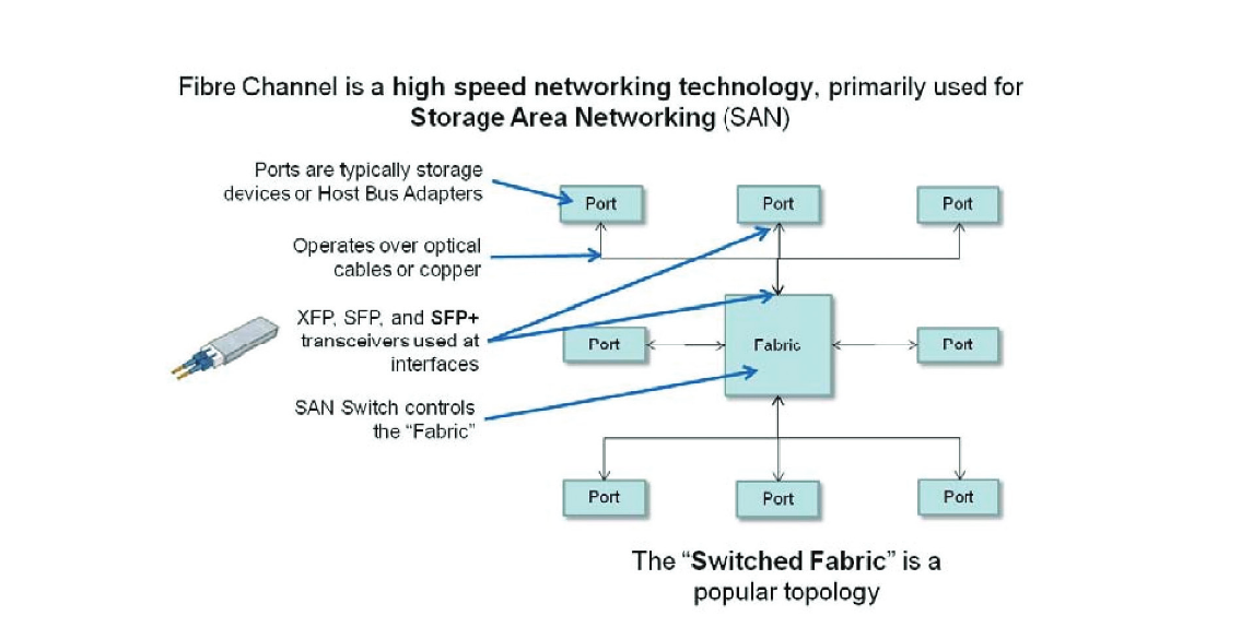
Fibre Channel (FC) is a high speed networking technology primarily used for Storage Area Networking (SAN). Devices on an Fibre Channel network are typically storage devices, Host Bus Adapters (HBA) connected to computers or servers, or as in the example "Switched Fabric" topology in Figure 1, a SAN Switch, which controls the "Fabric", or state of the Fibre Channel network by optimizing the connections between ports. The ports and switches use transceivers such as XFPii (10 Gigabit Small Form Factor Pluggable), SFPiii (Small Form Factor Pluggable) used for 4G and lower Fibre Channel applications, or SFP+vi used for 8GFC and 10 Gigabit Ethernet (GbE) applications (and will be used for 16GFC too), to interface to the Fibre Channel network. Fibre Channel supports either copper or optical cabling, but optical connections will be the focus of this paper.
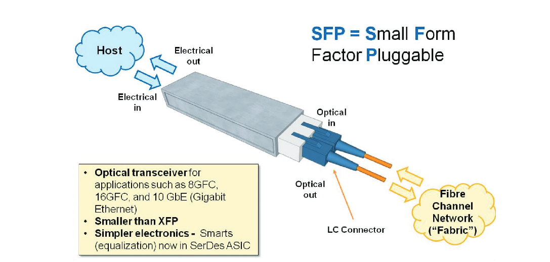
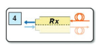
SFP+ is one type of transceiver found on a Fibre Channel network. As shown in Figure 2, it has an electrical interface to the host electronics, and an optical interface to the Fibre Channel network. The SFP+ is a more simplified transceiver module than its 10 GbE predecessor, the XFP optical module, moving some of the electronics out of the module and onto the line card with the serializer/deserializer (SerDes)/physical layer (PHY) functions, electronic dispersion compensation (EDC), and signal conditioning. As a result, the modules are smaller, consume less power, allow increased port density, and are less expensive compared to XFP.
Historically, SFP+ devices have not included clock and data recovery (CDR) circuitry, leaving that to the downstream IC. However, many SFP+ designs targeting 16GFC will include CDR circuitry inside the transceiver, at least on the receiver side. This will help clean up the signal for the downstream host ASIC, since jitter within the CDR loop bandwidth will be tracked out.
1.1 Interpreting the Standards
There are separate standards for Fibre Channel and SFP+.
- The Fibre Channel standardiv, Fibre Channel Physical Interface-5 (FC-PI-5), September 25, 2008 is in draft form as of December 1, 2009 (the latest document, 09-392v1, is available on the t11 website (www.t11.org), dated Nov 17, 2009). It includes the 16G specifications and carries forward from its precursor, Fibre Channel Physical Interface-4v (FC-PI-4).
- The SFP+ standardvi, SFF-8431 Specifications for Enhanced Small Form Factor Pluggable Module SFP+, rev 4.1, July 4, 2009 does not include mention of 16G Fibre Channel.
For 8GFC environments, the SFP+ standard explicitly defers to the Fibre Channel standard. We will assume that it will do the same for 16GFC, and thus, we will use the latest publicly available draft of the Fibre Channel FC-PI-5 standard for testing an SFP+ device in this paper.
In general, the specifications for 16G in the Fibre Channel standard are mostly complete (although subject to change), with many test methodologies referring to the incomplete Fibre Channel - Methodologies for Signal Quality Specificationvii (MSQS) document. For the purposes of this paper, previous standards such as the FC-PI-4 and the Fibre Channel - Methodologies for Jitter and Signal Quality Standardviii (MJSQ) will be consulted in cases where measurement methodologies are unavailable in the FC-PI-5 and MSQS documents.
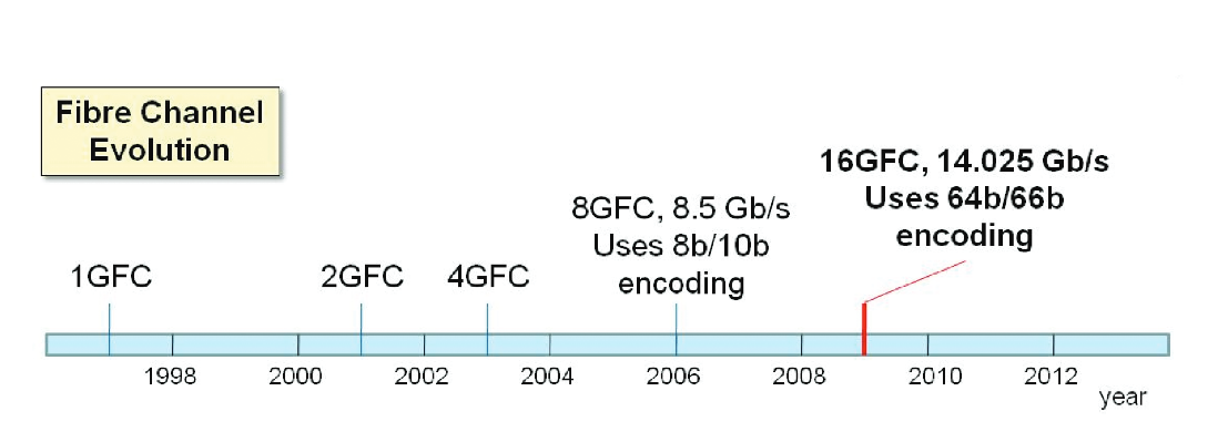
To understand more about the 16G specifications, it is helpful to look at the evolution of the Fibre Channel standard. As shown in Figure 3, besides the data rate, the big difference between 8G Fibre Channel and 16G Fibre Channel is the encoding method. 64b/66b encoding used for 16G is a more efficient encoding mechanism than 8b/10b used for 8G, and allows for the data rate to double without doubling the line rate. The result is the 14.025 Gb/s line rate for 16G Fibre Channel.
The other area impacted by the encoding method is the compliance data pattern. Since both the FC-PI-5 and FCMSQS are still in draft, the data patterns to use for testing are not always clear. For now, data patterns used for 8GFC testing and those used in other high speed standards that use 64b/66b encoding should be turned to for clues.
- JSPAT is widely used for 8G Fibre Channel.
- PRBS-9 is used for SFP+.
- PRBS-31 is used for 10 Gb and 100 Gb Ethernet
A combination of all three data patterns will be used in the upcoming example.
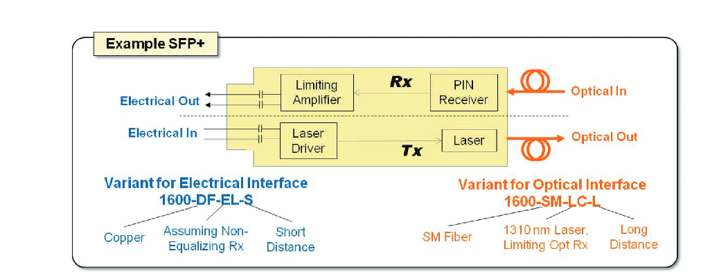
When interpreting the Fibre Channel standard, one must identify the correct "variants" to use. Variants are used in the specifications tables to direct readers to the sections of the tables that pertain to their device’s interfaces. The standard supports numerous variants, each defined by four categories:
- Speed – 1G, 2G, 4G, 8G, or 16G. This paper focuses on 16G.
- Transmission media – single mode (SM) or multi-mode (MM) optics, or copper
- Interoperability type – a wavelength specific laser with limiting or linear optical receiver, or electrical with or without downstream equalization
- Distance – up to 70 m (short) to 50 km (very long)
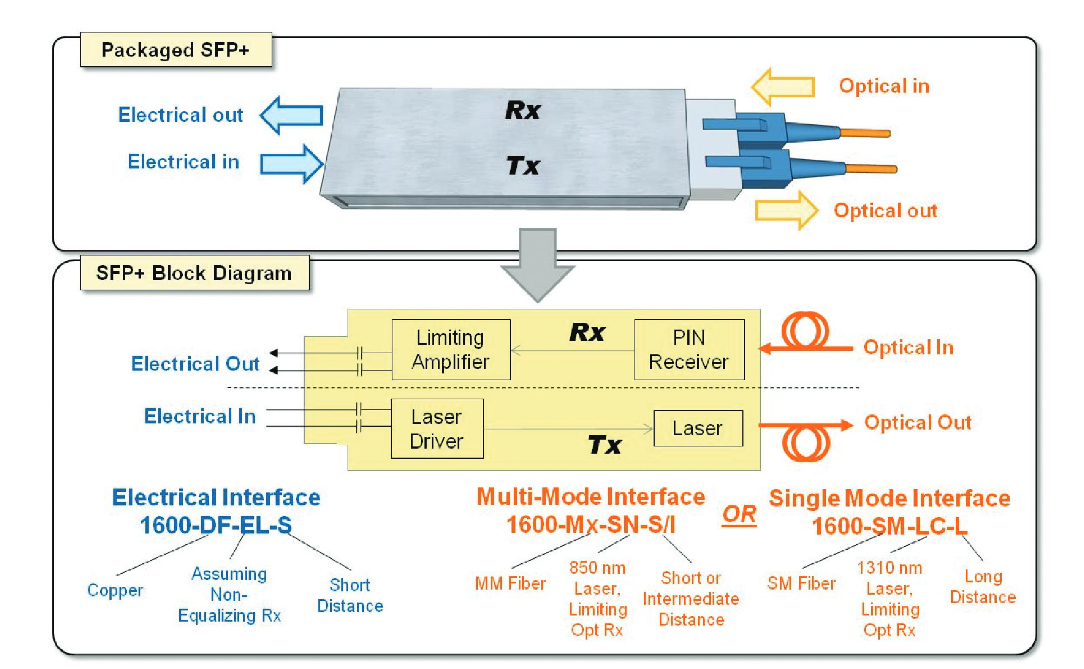
An example SFP+ block diagram is shown in Figure 4. There are two types of interfaces – the electrical side interfaces with electronics on the host, and the optical side interfaces with the optical network. The electrical interface must be tested using an electrical variant. The example shown assumes a nonequalizing downstream receiver. On the optical side, SFP+ devices can operate over multi-mode or single mode optical fiber, depending on the wavelength of the laser. Example multi-mode and single mode variants are shown for the optical interface in Figure 4.
Single mode fiber typically operates over longer distances than multi-mode fiber and requires more expensive optical components to drive it. Multi-mode fiber is limited to shorter distances, often within a building. Less expensive optical drivers such as LEDs (light emitting diodes) or VCSELs (vertical cavity surface emitting lasers) can be used for multi-mode operation.
The variants and their specifications will be discussed in depth in Chapter 2, ‘Test Specifications for an SFP+ Optical Transceiver’, and used in Chapter 3, ‘Example – 1310 nm Laser, Single Mode Fiber Variant’.
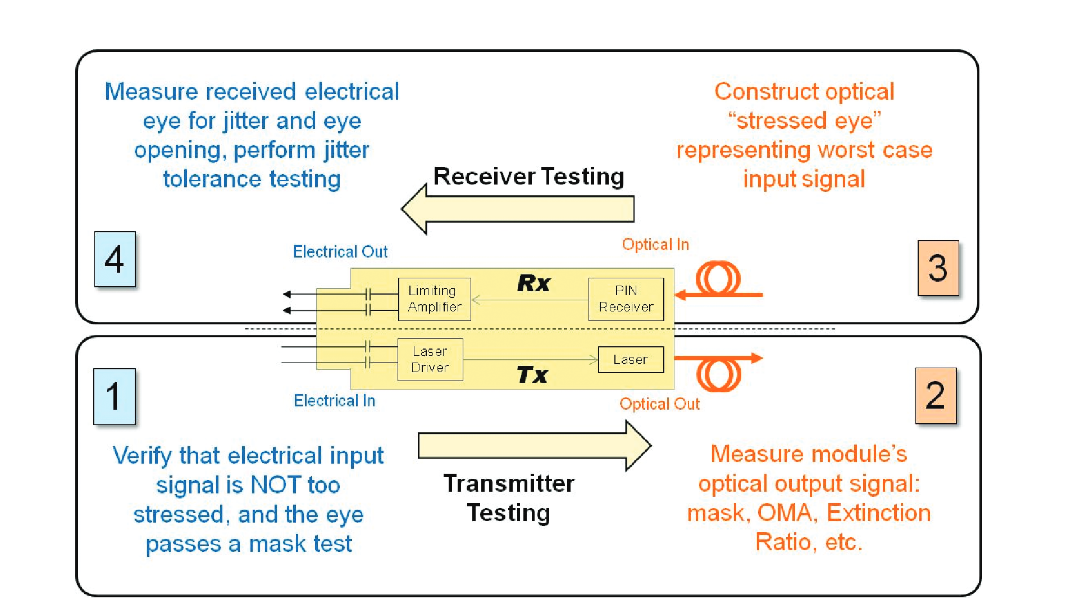
1.2 Overview of Testing an Optical Transceiver
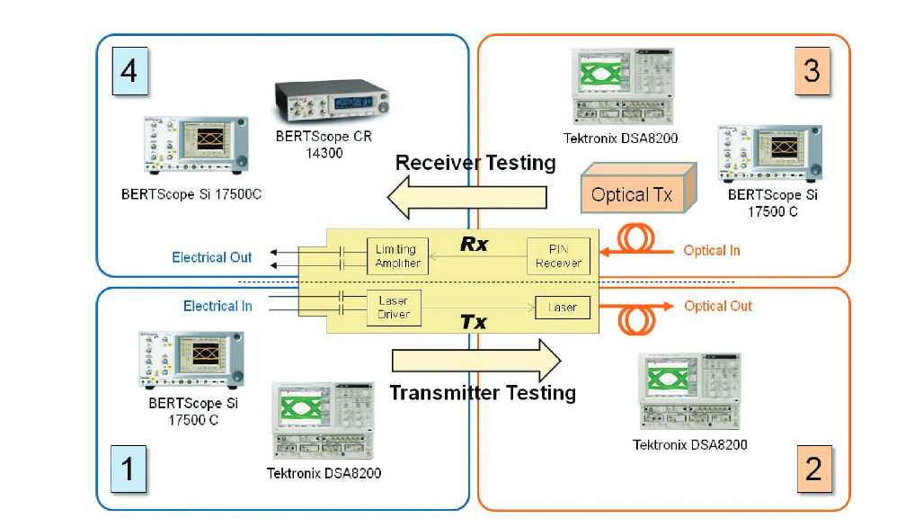
There are four basic steps in testing an SFP+ transceiver, as shown in Figure 5. These four steps will be referred to throughout the remainder of this paper. The icons below will be used as a navigation aid in the upcoming example.
1.2.1 Transmitter Testing:
1. The input signal used to test the transmitter must be good enough.Measurements of jitter and an eye mask test must be performed to confirm the quality using electrical measurements.
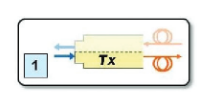
2. The optical output of the transmitter must be tested using several optical quality metrics such as a mask test, OMA (optical modulation amplitude), and Extinction Ratio.
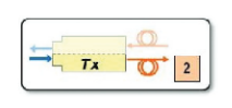
1.2.2 Receiver Testing
3. Unlike testing the transmitter, where one must ensure that the input signal is of good enough quality, testing the receiver involves sending in a signal that is of poor enough quality. To do this, a stressed eye representing the worst case signal shall be created. This is an optical signal, and must be calibrated using jitter and optical power measurements.
4. Finally, testing the electrical output of the receiver must be performed. Three basic categories of tests must be performed:
- A mask test, which ensures a large enough eye opening.The mask test is usually accompanied by a BER (bit error ratio) depth.
- Jitter budget test, which tests for the amount of certain types of jitter.
- Jitter tracking and tolerance, which tests the ability of the internal clock recovery circuit to track jitter within its loop bandwidth.
2. Test Specifications for an SFP+ Optical Transceiver
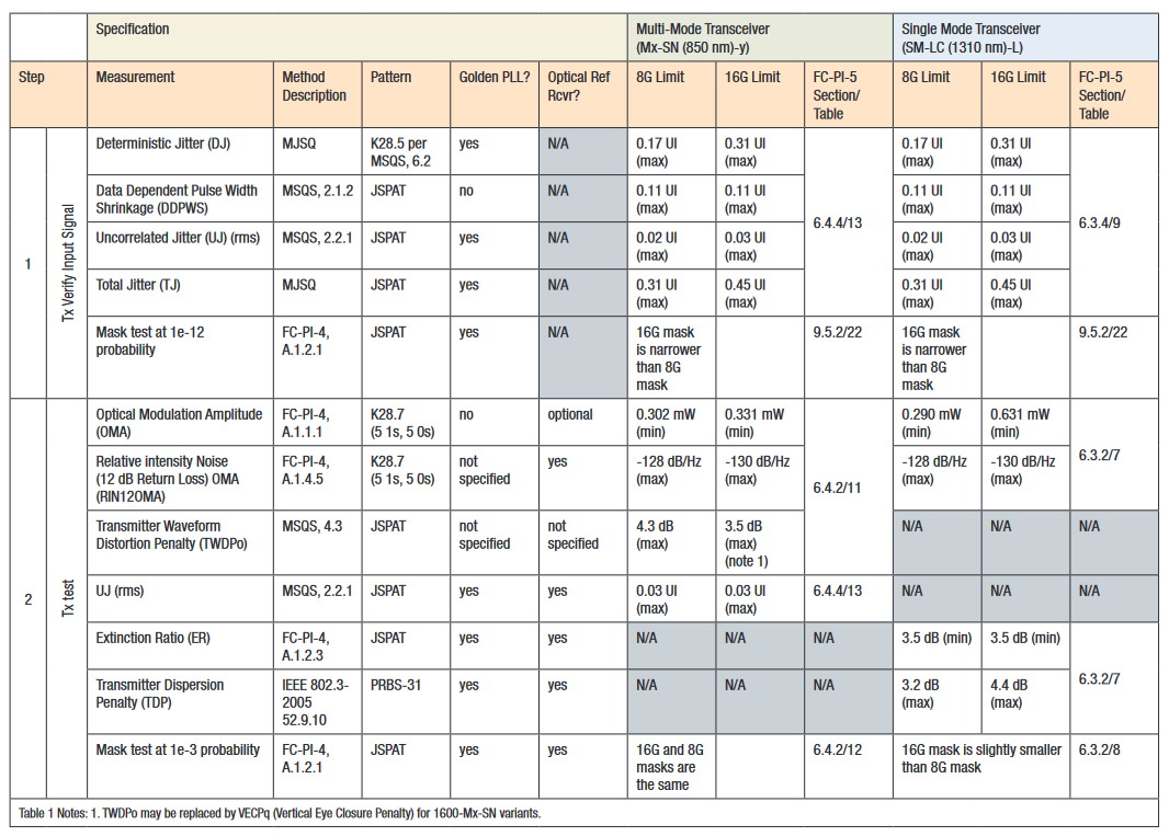
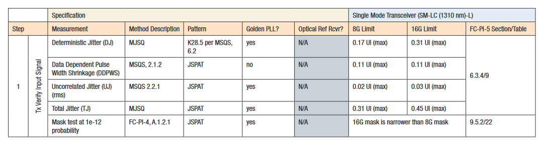
In this section, the specifications for testing an SFP+ optical transceiver will be examined, following steps 1-4 as just outlined. This section will address both types of optical interfaces – namely, an 850 nm laser operating over multimode fiber, and a 1310 nm laser operating over single mode fiber. Table 1 outlines the transmitter test specifications . For each measurement, the following information is included:
The location in the specifications of the measurement methodology. As previously mentioned, there are currently many references in FC-PI-5 to methodologies that will be in MSQS, but at the moment do not exist. However, many of these methodologies exist in FC-PI-4, which is why many entries Table 1 and Table 2 refer to FC-PI-4.
The data pattern is often specified in the measurement methodology. In some instances, the test pattern is not explicitly stated, and a best guess has been used.
For many measurements, a Golden PLL with cutoff frequency of data rate/1667 is required.
For optical measurements, an optical reference receiver with 4th Order Bessel-Thompson filter with bandwidth 0.75 x data rate is often required. This does not apply to electrical measurements.
The specifications for testing the electrical input to ensure good enough quality (Step 1) are almost identical between the MM and SM variants. The 16G limits are more relaxed compared to the 8G limits. For example, the acceptable amount of Total Jitter (TJ) that can be input to the transmitter is 0.45 UI for 16G compared to 0.31 UI for 8G, placing a higher burden on the transceiver to generate a decent optical output signal.
The measurements required in Step 2, transmitter output testing, are slightly different between the MM and SM variants. In general terms, SM fiber does not suffer from modal dispersion as much as MM fiber, and as such, can maintain the fidelity of the transmitted signal over longer distances. This is reflected in the particular set of requirements for each.
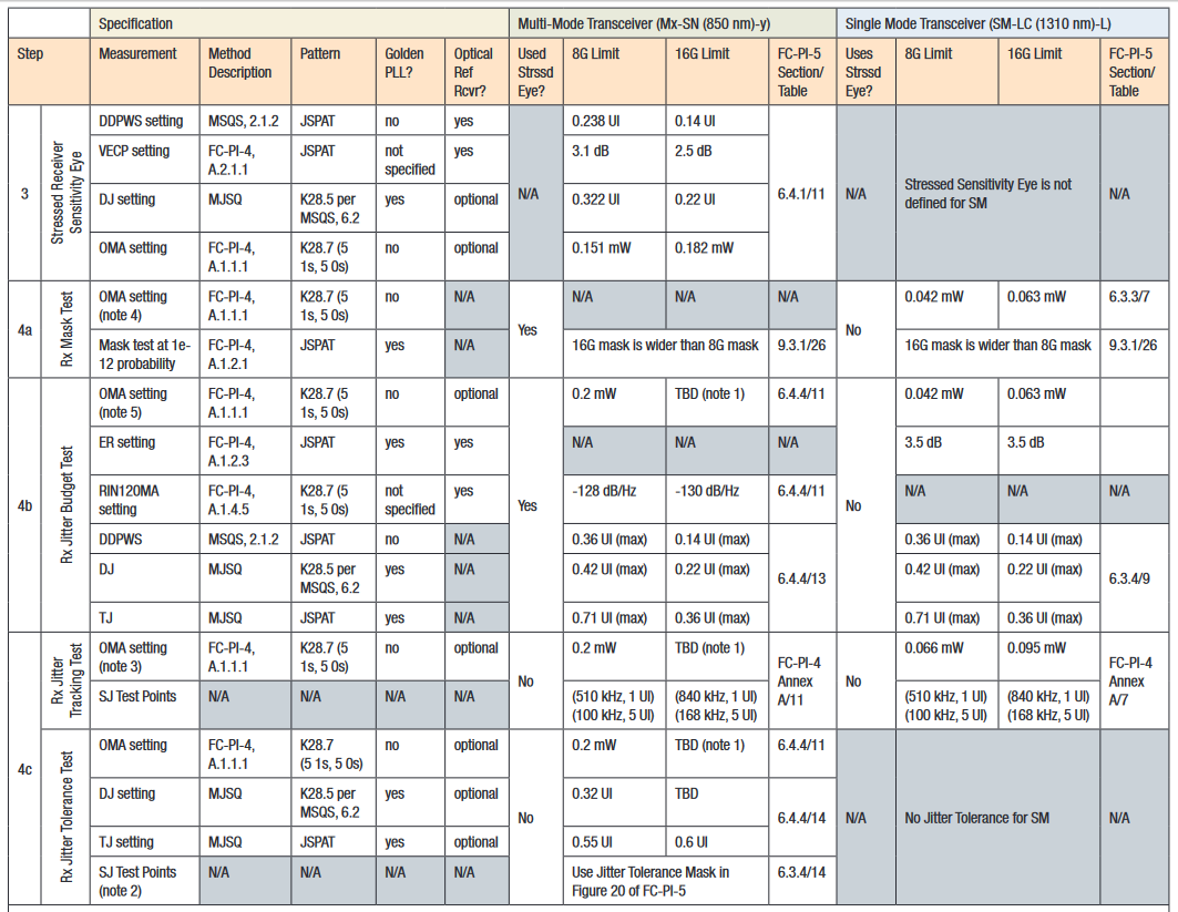
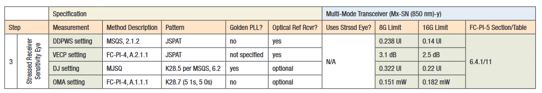
In Table 2, there are more differences between the MM and SM variants for receiver testing compared to those for transmitter testing. The biggest difference is that there is no receiver stressed sensitivity eye (Step 3) specifications for SM. Whereas the MM variant is tested with a stressed eye for the Eye Mask (Step 4a) and Jitter Budget (Step 4b) tests, the SM variant is tested with an unstressed eye that is impaired vertically with a low OMA setting.
The Jitter Tracking test (Step 4c) is the main test for the clock recovery circuit that will likely be in SFP+ transceivers operating at the 16G rate. The SM variant does not have any specifications for Jitter Tolerance, and it is possible that the MM variant does not require it either (see note 2 of Table 2). The Jitter Tracking test does not require a stressed eye, and uses a higher OMA setting than the Eye Mask and Jitter Budget tests. The Jitter Tolerance test for MM variants uses a stressed eye recipe that is slightly different from the stressed eye in Step 3.
The test methodologies and measurements for the 16G SM variant will be covered in more detail in the following example. All measurements required for the MM variant as well as an 8G compliance testing example are covered in the predecessor to this application note, “Testing an SFP+ Transceiver to the 8x Fibre Channel Specificationsix”.
3. Measurement Example – 1310 nm Laser, Single Mode Fiber Variant
The goal of this example is to demonstrate test and characterization of an SFP+ device to the 16G Fibre Channel standard using state of the art test equipment. The goal is not to show how the device can pass all the specifications; rather, the intent is to show the methodologies and tools one can use to accomplish 16G Fibre Channel testing and characterization with a Tektronix BERTScope.
3.1 SFP+ Device Under Test (DUT)
This example uses a prototype SFP+ device designed for 10 Gb Ethernet applications, but pushed to the 14.025 Gb/s data rate of 16G Fibre Channel. It does not include CDR circuitry, so the Jitter Tracking and Tolerance methods will be covered, but not demonstrated.
Inside, the SFP+ DUT has a limiting amplifier in the receiver, and a 1310 nm laser in the transmitter designed to operate over single mode optical fiber. For testing the electrical interface, the variant 1600-DF-EL-S is used, and for the optical interface, the variant 1600-SM-LC-L is used, as shown in Figure 6. The specifications in Table 1 and Table 2 will be referred to throughout the example.
3.2 14.025 Gb/s Capable Test Equipment
Characterizing and testing an SFP+ device requires a set of equipment that can produce and measure optical and electrical signals at 14.025 Gb/s. Signal generation and measurements at 14.025 Gb/s can be accomplished by the following set of test equipment.
1. The BERTScope BSA175C operates up to 17.5 Gb/s and includes both a stressed pattern generator and a BERbased signal measurement system.
- a. The generator can provide a differential electrical signal for transmitter testing, and paired with an optical transmitter, it can provide the stressed signal for receiver testing.
- b. The BER-based detector can perform electrical analyzer functions, such as eye measurements and eye mask tests, jitter decomposition, and jitter tolerance tests.
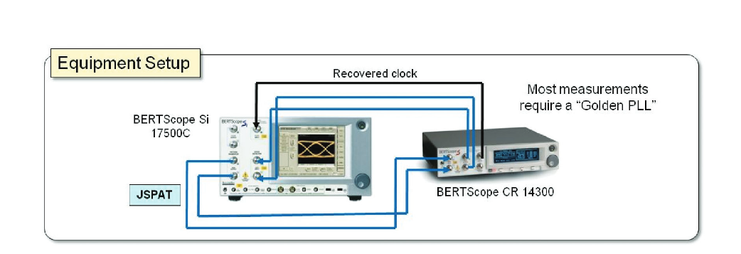
2. The BERTScope CR175A provides compliant clock recovery up to 17.5 Gb/s1 with configurable loop bandwidth and peaking settings. Many measurements, such as jitter measurements, require the use of a Golden PLL, provided by the BERTScope CR.
3. The Tektronix DSA8200 is a digital sampling oscilloscope. It can perform full jitter and noise decomposition as well as eye diagram measurements. Equipped with an 80C11 Optical Reference Receiver, the DSA8200 can perform both electrical and optical measurements.
3.3 Transmitter Testing
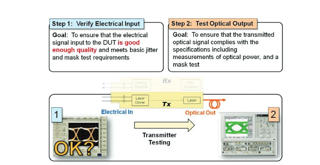
This example will begin with testing the transmitter, composed of two steps (1 and 2). The input signal is verified in Step 1 (the DUT is not needed for this step), and the DUT’s transmitter is tested in Step 2.
3.3.1 Transmitter Testing Step 1 – Verify Electrical Input Signal
In Step 1, the input signal to the DUT must be tested to ensure a quality signal input to the transmitter. To verify the electrical signal, the setup shown in Figure 9 was used.
The measurements and limits for 16G transmitter input verification are shown in Table 3 along with its 8G predecessor for comparison. Note that the limits for 16G are more lenient than those for 8G.
All measurements listed in Table 3 are demonstrated in the following sections, along with a brief definition of each measurement.
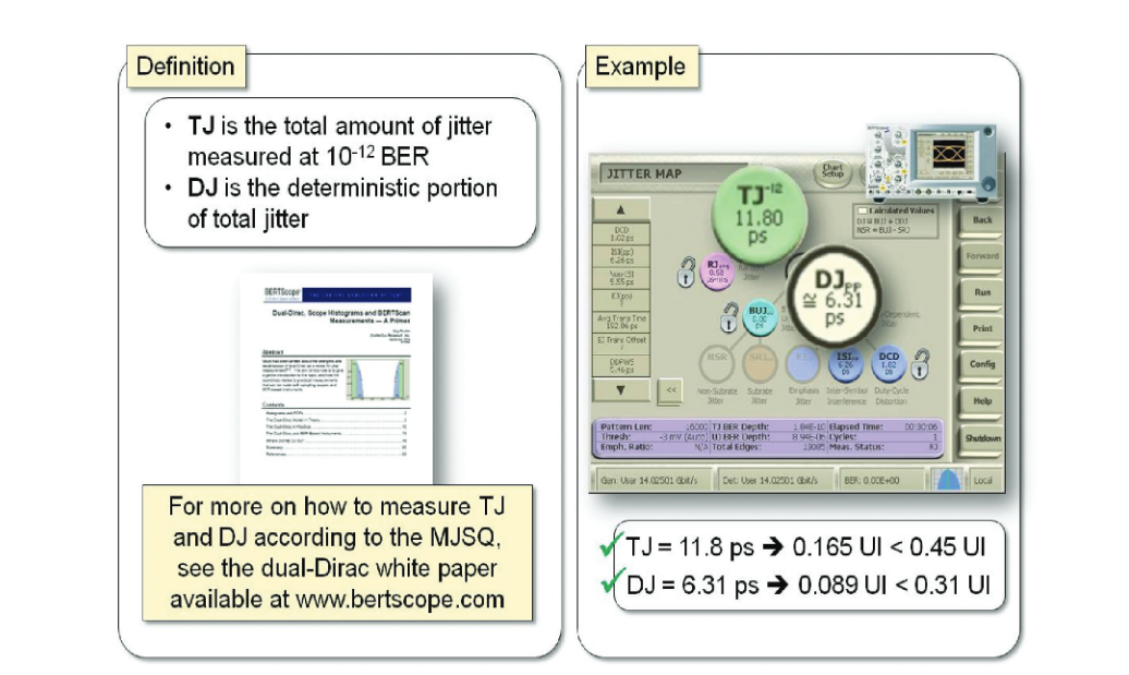
3.3.1.1 Deterministic Jitter (DJ) and Total Jitter (TJ)
In Figure 10, TJ and DJ were measured on the BERTScope using the Jitter Map jitter decomposition feature. Details on the methods used to measure jitter can be found in several sources, including the MJSQvii, and the dual-Diracx and Jitter Mapxi white papers available from the BERTScope website.
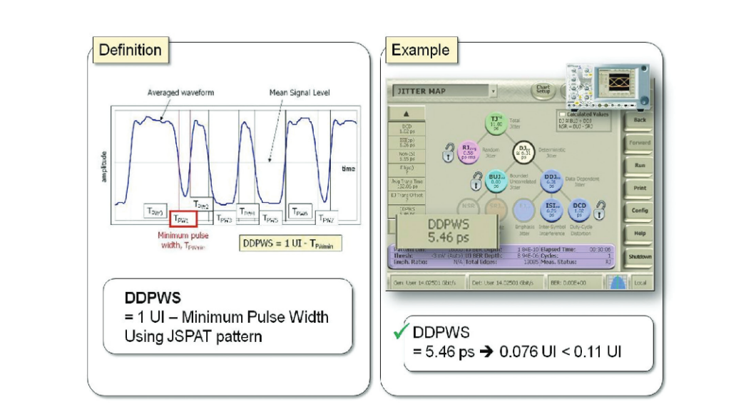
3.3.1.2 Data Dependent Pulse Width Shrinkage (DDPWS)
The DDPWS measurement is similar to the Data Dependent Jitter (DDJ) measurement in that it captures the amount of eye closure due to inter-symbol interference (ISI) and duty cycle distortion (DCD). It differs from DDJ in cases of overequalization where there is overcompensation for ISI from transmitter pre- emphasis or receiver equalization. This can improve DDPWS at the expense of DDJ.
The DDPWS measurement is based on an averaged waveform, as shown in Figure 11, and is the difference between one unit interval and the shortest pulse width, as measured on a JSPAT data pattern. In this example, the amount of measured DDPWS passes the requirement for the transmitter input signal.
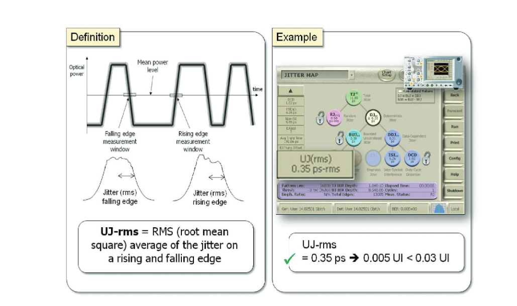
3.3.1.3 Uncorrelated Jitter (UJ)
The UJ-rms measurement is one based on jitter histograms or probability density functions (pdf) of a rising and falling edge of the data pattern. The standard deviations of the two histograms are RMS- averaged to create the UJ-rms measurement. According to MSQS, the JSPAT pattern can be used to measure UJ-rms (although the particular rising and falling edges in the pattern are not specified). BERTScope BSA175C’s Jitter Map includes a UJ-rms measurement, as shown in Figure 12. The measured UJ-rms is below the specified limit.
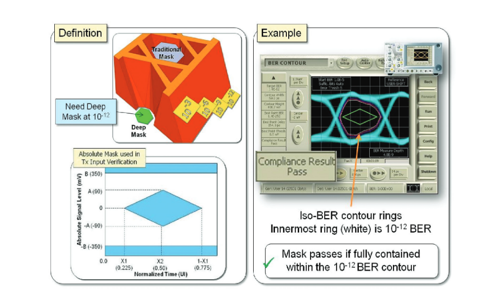
3.3.1.4 Mask Test
A mask test is performed by comparing a keep out region to an eye diagram. If no part of the eye diagram crosses the mask, then the mask test passes. Typical eye diagrams are relatively shallow, however, and usually include sample waveforms numbering in the thousands, equating to a BER of approximately 10-3. For a more stringent test, masks can be accompanied by a sample depth requirement, as in this case where a depth of 10-12 BER is required.
The BERTScope accomplishes deep mask testing in its Compliance Contour tool, which performs a deep extrapolation of the eye opening down to 10-12 BER or below, and compares a mask to the opening at a specific BER level. In the example in Figure 13, the mask must be compared to the eye opening at 10-12 BER, which is the white innermost ring. The mask does not cross into this ring and the mask test passes.
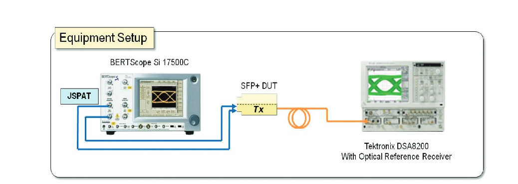
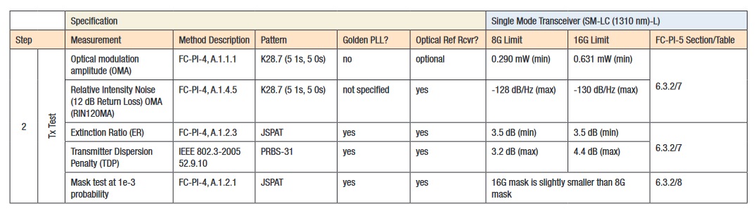
Table 4. Specifications for Transmitter Optical Output Testing – SM Variants.
For Step 2, the optical output signal of the DUT’s transmitter must be tested to ensure that the transmitter can generate a good quality signal. To verify the optical signal, the equipment setup was as shown in Figure 14. JSPAT continued to be the data pattern used. All optical measurements were taken using the Tektronix DSA8200 Sampling Oscilloscope.
The measurements and limits for 16G transmitter output testing are shown in Table 4 along with its 8G predecessor for comparison. Note that the limits for 16G are more stringent that those for 8G, especially the OMA. Demonstrations of RIN12OMA and TDP are beyond the scope of this example.
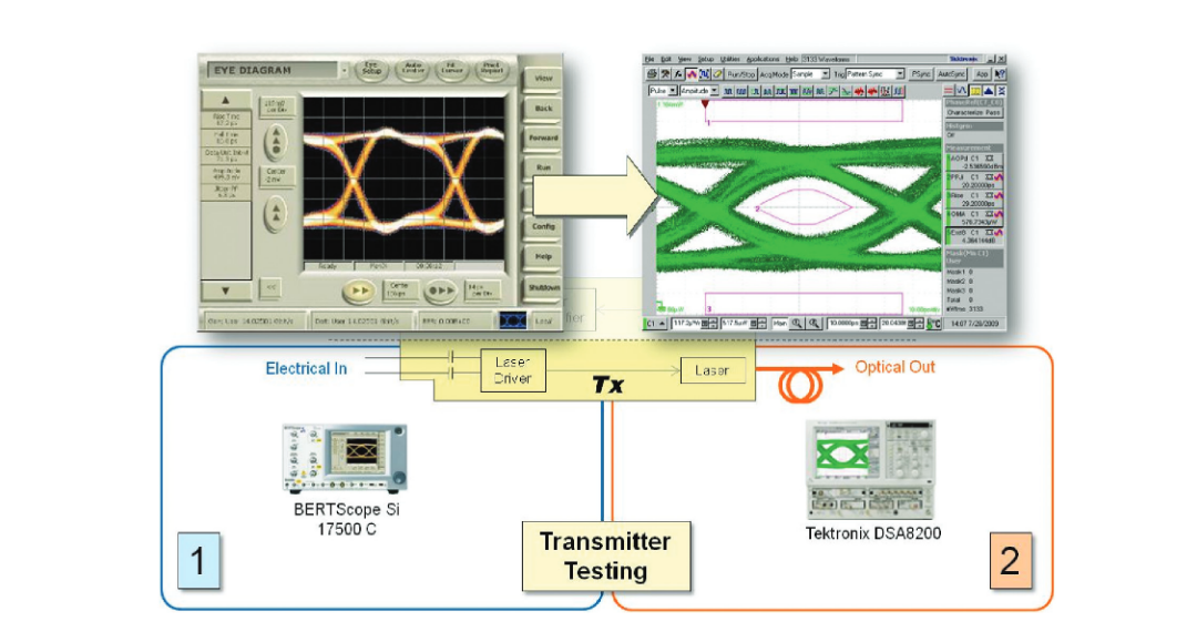
3.3.2.1 Comparison of Input and Output Eye Diagrams
First, it is helpful to compare the electrical signal going into the transmitter, with the optical signal coming out. Figure 15 compares the input and output eye diagrams. There is some slowing of the rise and fall time of the output waveform compared to the input waveform. Remember that the DUT was one designed for 10 Gb/s operation, being pushed to 14.025 Gb/s in this example.
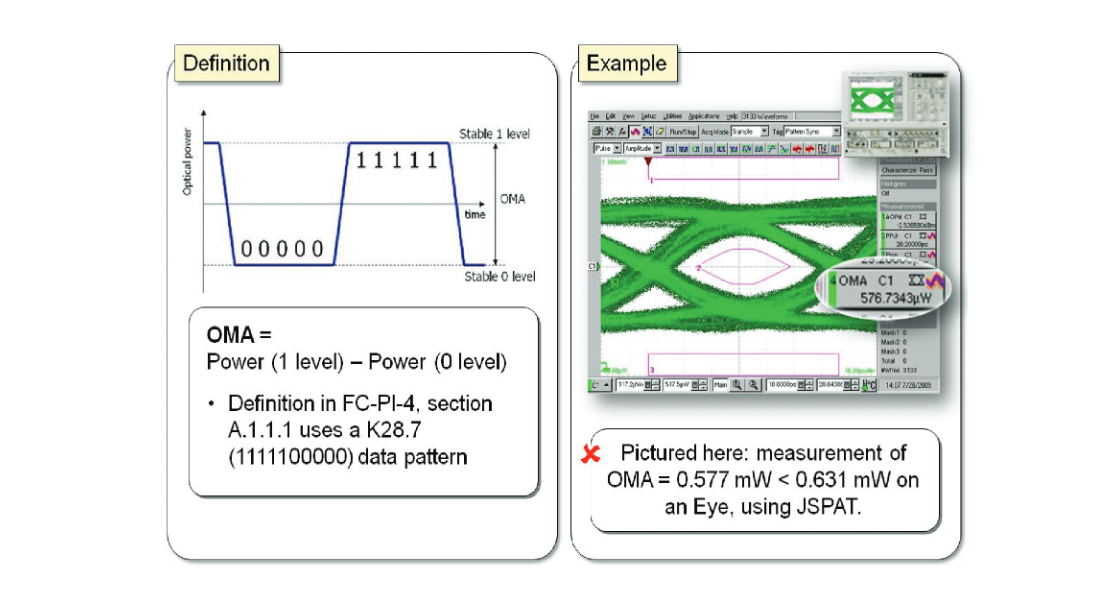
3.3.2.2 Optical Modulation Amplitude (OMA)
OMA is a measurement of the optical power and is specified in FC-PI-4 to be measured on a square wave data pattern (K28.7, or repeating 1111100000). This example shows the measurement on a JSPAT pattern. The measured value is lower than the minimum OMA.
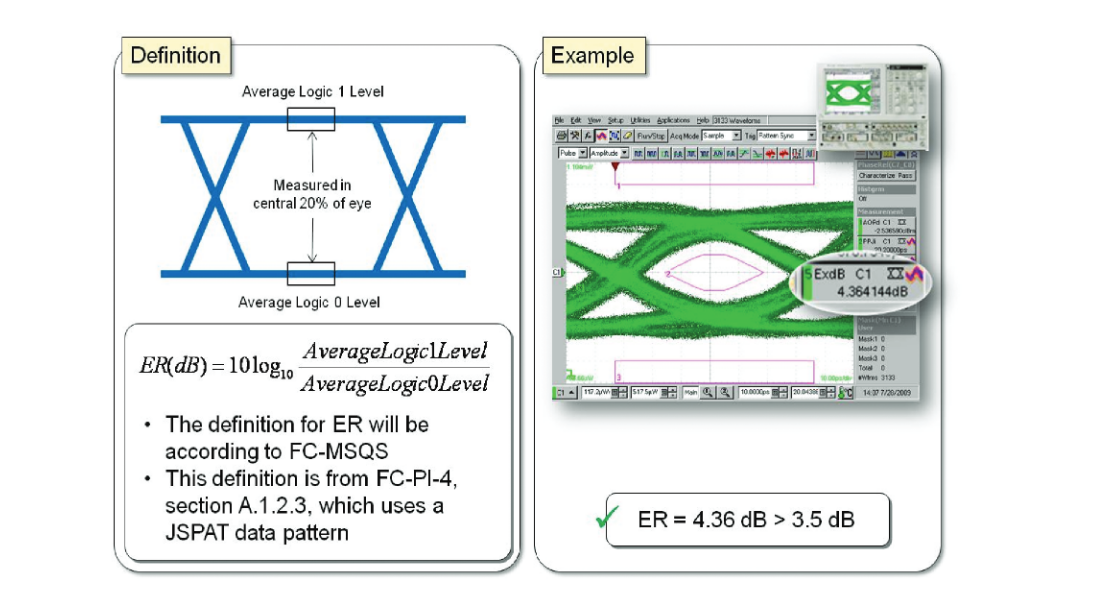
3.3.2.3 Extinction Ratio (ER)
The extinction ratio is another optical power measurement, defined as the ratio of the logic one power level to the logic zero power level, expressed in dB. It is a measure of efficiency – the higher the extinction ratio, the less average optical power is needed to maintain a constant level of BER at the receiver. The passing measurement is shown on the Tektronix DSA8200.
3.3.2.4 Mask Test
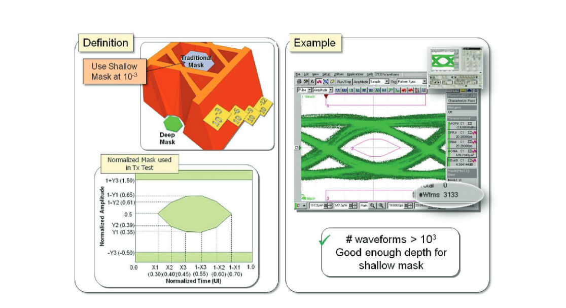
Figure 18 shows another mask test, similar to the mask used in Step 1, Transmitter Input Verification, in Figure 13. However, the mask used here in Step 2, Transmitter Optical Output Testing, is a shallow mask, defined at a BER of 10-3 instead of a deep mask defined at 10-12 BER, which was used in Step 1.
To perform a shallow mask test, a sufficient number of waveforms can be captured in the eye diagram directly and compared to the mask. This is in contrast to the need to extrapolate to 10-12 BER for deep mask testing, as seen in Figure 13. Figure 18 shows a total of 3133 waveforms, and the signal passes the shallow mask test at 10-3 BER.
3.4 Receiver Testing
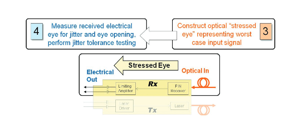
Like transmitter testing, receiver testing involves setting up and measuring the input signal to the receiver (Step 3) and then testing the output of the receiver (Step 4). Unlike transmitter testing, the signal input to the receiver is a worst case signal, typically called a “stressed eye”; its intent is to challenge the receiver to ensure operation at a BER of 10-12 or better under stressed signal conditions.
Previously, it was discussed that one big difference between the MM and SM variants was that the SM variant did not require a stressed eye to be created. However, because this is a critical step in testing MM variants, it will be covered in this example. In Step 3, we will create an optical stressed eye, and in Step 4, we will use it for testing and characterization of an SFP+ receiver, using it as a vehicle to aid in understanding how to make the various measurements involved in all aspects of testing an optical receiver to the 16G Fibre Channel cifications.
3.4.1 Receiver Testing Step 3 – Create Optical Stressed Eye (For MM Variants)
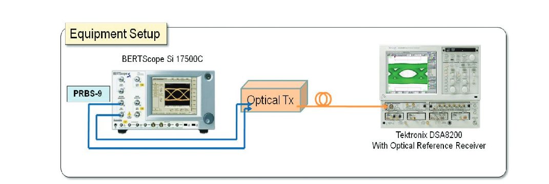
In Step 3, the receiver optical stressed eye will be created using the setup in Figure 20. The BERTScope generates the stressed electrical signal. After the signal gets converted to an optical stressed signal, it is measured by the Tektronix DSA8200 with optical receiver to ensure proper stressed signal conditions.
It is important to measure the signal input to the receiver. As seen in Figure 20, there are many components, both active (in the optical transmitter) and passive (electrical and optical cables) in between the originating electrical signal and the optical signal input to the receiver. These can have an impact on the eye opening in both the horizontal and vertical directions
Note that the data pattern used in Steps 3 and 4 for receiver testing is PRBS-9 instead of JSPAT. Recall that many test methodologies have yet to appear in MSQS. PRBS-9 was used in this example to show another possible data pattern that may eventually be used in FC-PI-5 and MSQS.
In creating a stressed eye, there is a recipe of impairments that must be followed. The recipe in the Fibre Channel standard for Multi-Mode is shown in Table 5. Single Mode variants do not require a stressed eye recipe. However, we include the calibration of a stressed eye in this example since it is a good illustration of how to perform the necessary measurements.
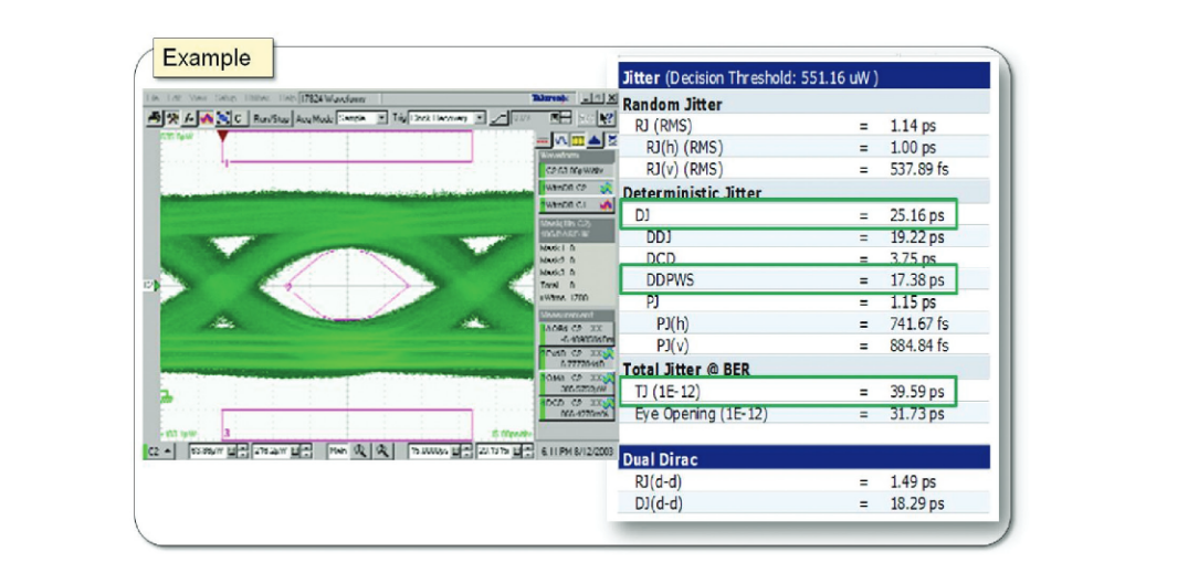
3.4.1.1 Jitter and OMA
These measurements were conducted at a time when the standard was still in its early stages of completion. The stressed eye recipe was derived from the 10 Gb Ethernet standard. Its targets were:
- DJ = 0.3 UI (16GFC requires 0.22)
- DDPWS = 0.24 UI (16GFC requires 0.14 UI)
- TJ = 0.55 UI (16GFC doesn’t include a TJ measurement)
- OMA = 0.2 mW (16GFC requires 0.182 mW)
As shown in Figure 21, the optical stressed eye meets the intended target values for DJ, DDPWS, TJ, and OMA, as measured on the Tektronix DSA8200. The stressed eye created had more jitter than the 16G Fibre Channel standard, but a higher OMA.
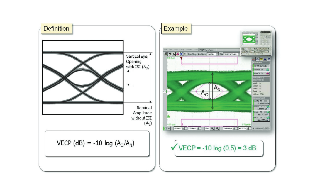
3.4.1.2 Vertical Eye Closure Penalty
The Vertical Eye Closure Penalty (VECP) is a measure of how much eye closure is created by Inter- Symbol Interference (ISI), and is represented as the ratio of the vertical eye opening with ISI, and the nominal amplitude without ISI. The VECP in this example is approximately 3 dB, as shown in Figure 22.
3.4.2 Receiver Testing Step 4 – Mask, Jitter Budget, and Jitter Tracking/Tolerance
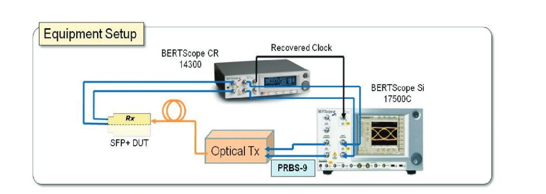
In Step 4, the electrical output of the DUT is measured by the electrical reference receiver and measurement system, the BERTScope CR 14300 and the BERTScope Si 17500C respectively. Optical input signal conditions depend on the test being performed.
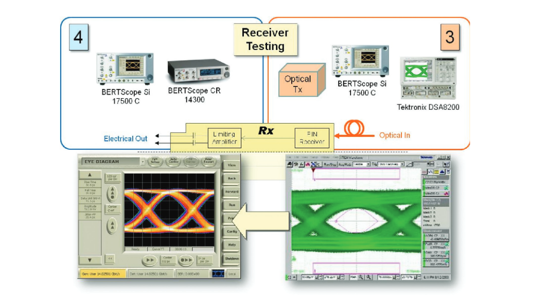
3.4.2.1 Comparison of Input and Output Eye Diagrams
As an initial test, the input and output eyes from the receiver are compared in Figure 24 using the stressed eye setup in Step 3. From the appearances of the output eye diagram, which demonstrates a fairly open eye, the receiver should be able to operate within its BER objectives. However, only shallow eye diagrams are shown. A deep mask test (next) will be examined to ensure confidence in meeting the BER objective.
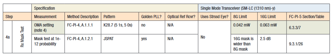
3.4.2.2 Receiver Testing Step 4a – Mask Test
To test an SM variant receiver, instead of a stressed eye, an input signal with low OMA should be used. However, this example went beyond compliance and used the stressed eye signal created in Step 3.
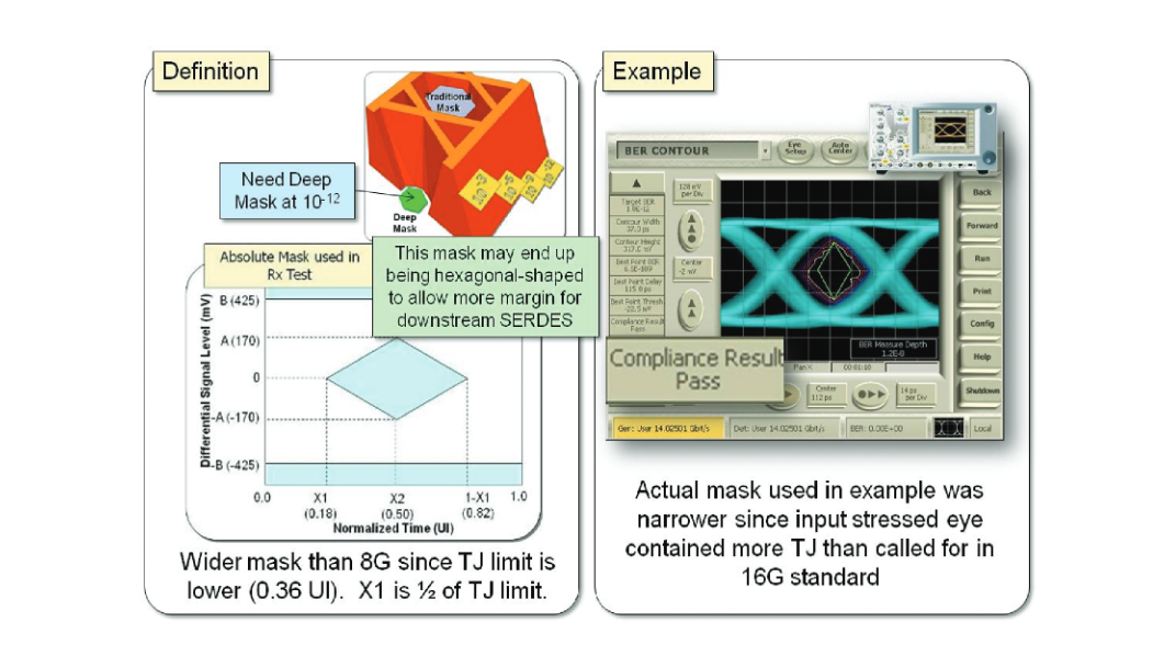
The mask specified in the Fibre Channel standard for 16G is slightly wider than that for 8G operation. It is shown in Figure 25. Note that the width of the mask is dictated by the TJ specifications, which are more stringent for 16G (0.36 UI) than for 8G (0.71 UI). The mask is a deep mask test, defined at a BER of 10-12 .
The mask used to test the output of the receiver in this example was narrower than that in the current standard, due to the added stress injected into the optical input signal in Step 3. Nonetheless, the DUT shows that it has a very clear 10-12 BER opening, passing the deep mask test with the modified mask.
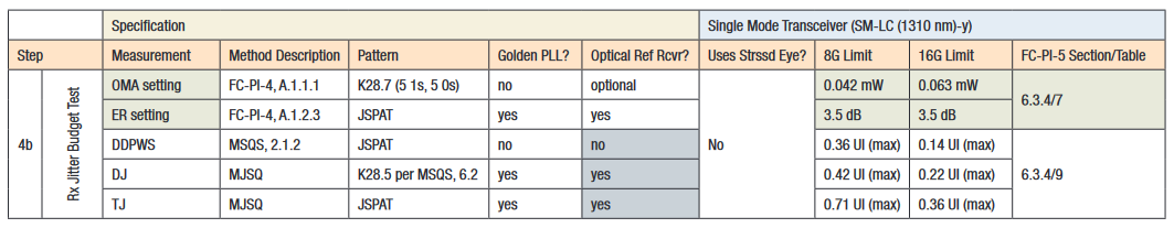
3.4.2.3 Receiver Testing Step 4b – Jitter Budget
This step tests jitter measured at the output of the receiver. Table 7 shows the SM limits for jitter. Note that the 16G limits are more stringent (lower) than those for 8G. This is why the 16G mask is wider than the 8G mask, as shown in the previous section (Step 4a) – the mask horizontal limits are dictated by the TJ specification in Table 7.
The standard requires an optical input test signal meeting OMA and ER requirements. However, as in the previous step (Step 4a), the stressed eye from Step 3 was used as input. Instead of comparing output jitter measurements to the specification, the output jitter will be compared to the input jitter, with the goal of characterizing DUT, and ensuring that it is not injecting too much additional jitter than exists in the input signal.
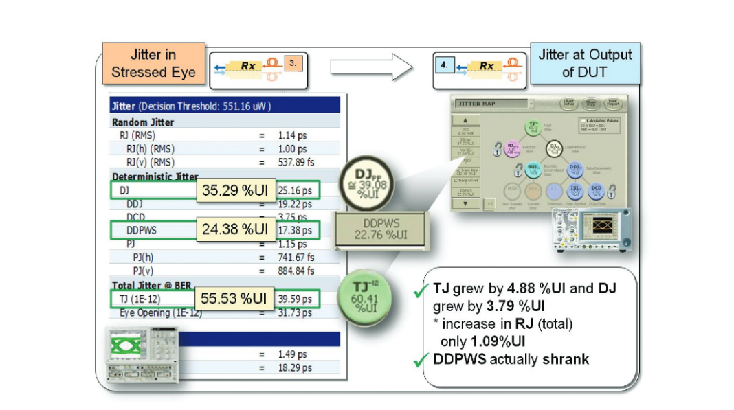
3.4.2.3.1 Jitter Comparison – Input to Output
The input and output jitter results are shown in Figure 26. The jitter in the stressed eye (left) is the same as shown in Step 3, measured on the optical stressed eye using the Tektronix DSA8200. The jitter in the output of the receiver (electrical) is shown on the right, measured by the BERTScope’s Jitter Map feature. TJ and DJ had modest increases of less than 0.05 UI, and the total amount of RJ only increased by 0.01 UI (the equivalent of an increase of 0.0007 UI of RJ-rms). The DDPWS measurement actually decreased. This imparts confidence that the jitter is not increasing significantly when the signal passes through the DUT.
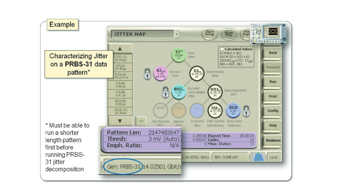
3.4.2.3.2 Jitter Decomposition on PRBS-31
In addition, Figure 27 shows how the BERTScope can decompose jitter on long data patterns such as PRBS-31 using the Jitter Map software option. Jitter Map can perform jitter analysis on patterns longer than PRBS-15 provided that it can first run on a shorter repeating data pattern (such as PRBS-7). While PRBS-31 may not end up being a compliance pattern for 16G Fibre Channel, as more interconnect standards move toward longer compliance patterns, the need to perform detailed jitter analysis on long patterns will likely grow.

3.4.2.4 Receiver Testing Step 4c – Jitter Tracking/ Tolerance
The final part of Step 4 is a jitter tracking/tolerance test. For SM variants, only the Jitter Tracking test is required. For MM variants, the Fibre Channel standard includes both jitter tracking and tolerance, but it is possible that only jitter tracking will be necessary. Nonetheless, both types of tests are discussed next.
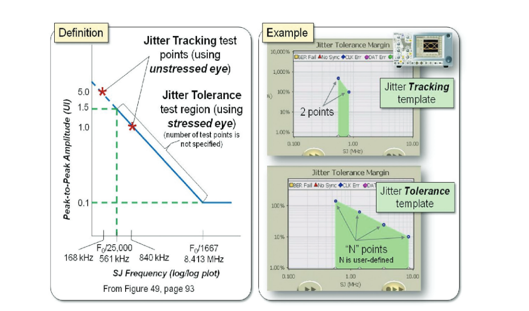
The goal of the jitter tracking test is to test the clock recovery circuitry of the receiver. Jitter tracking uses SJ frequencies that are well within the clock recovery loop bandwidth - 5 UI of SJ at 168 kHz, and 1 UI of SJ at 840 kHz. Clearly, with this amount of SJ amplitude, the receiver will generate errors if the clock recovery is not able to perform its job of tracking out the jitter. The input signal used for jitter tracking is not stressed. Instead, the OMA of the input signal is the only parameter specified.
Jitter tolerance for MM variants, on the other hand, uses an input signal that is similar to (but not exactly the same as) the stressed eye created in Step 3. The recipe is shown in Table 8. Jitter tolerance tests the SJ frequency range up to the corner frequency of the clock recovery, which is equal to the data rate divided by 1667. While jitter tracking uses only two test points, the number of test points for jitter tolerance testing is not specified – only the template shown in Figure 28 is specified.
Figure 28 shows how the jitter tracking and tolerance tests can be setup in the BERTScope using the automated Jitter Tolerance tool, which can test specific SJ frequencies and amplitudes for BER, yielding pass/fail results for testing, or find the amount of margin in the DUT by finding the SJ amplitude pass/fail threshold for each SJ frequency test point for characterization.
Summary
In this paper, an SFP+ device was characterized at the 16G Fibre Channel rate of 14.025 Gb/s, using the existing 16GFC standard as a guide. Using the BERTScope BSA175C, BERTScope CR 175A, and DSA8200 sampling oscilloscope with optical receiver, stressed signal generation and analysis for transmitter and receiver test and characterization was demonstrated. In particular, set up and calibration of an optical stressed eye for receiver test was shown, and used for testing and characterizing the SFP+ DUT by the BERTScope, including a deep eye mask test using Compliance Contour, jitter decomposition using Jitter Map, and jitter tracking/ tolerance testing using the automated Jitter Tolerance tool.