Resistivity Measurements of Semiconductor Materials Using the 4200A-SCS Parameter Analyzer and a Four-Point Collinear Probe
Introduction
Electrical resistivity is a basic material property that quantifies a material’s opposition to current flow; it is the reciprocal of conductivity. The resistivity of a material depends upon several factors, including the material doping, processing, and environmental factors such as temperature and humidity. The resistivity of the material can affect the characteristics of a device of which it’s made, such as the series resistance, threshold voltage, capacitance, and other parameters.
Determining the resistivity of a material is common in both research and fabrication environments. There are many methods for determining the resistivity of a material, but the technique may vary depending upon the type of material, magnitude of the resistance, shape, and thickness of the material. One of the most common ways of measuring the resistivity of some thin, flat materials, such as semiconductors or conductive coatings, uses a four-point collinear probe. The four-point probe technique involves bringing four equally spaced probes in contact with a material of unknown resistance. A DC current is forced between the outer two probes, and a voltmeter measures the voltage difference between the inner two probes. The resistivity is calculated from geometric factors, the source current, and the voltage measurement. The instrumentation used for this test includes a DC current source, a sensitive voltmeter, and a four-point collinear probe.
To simplify measurements, the 4200A-SCS Parameter Analyzer comes with a project that contains tests for making resistivity measurements using a four-point collinear probe. The 4200A-SCS can be used for a wide range of material resistances including very high resistance semiconductor materials because of its high input impedance (>1016 ohms). This application note explains how to use the 4200A-SCS with a four-point collinear probe to make resistivity measurements on semiconductor materials.
The Four-Point Collinear Probe Method
The most common way of measuring the resistivity of a semiconductor material is by using a four-point collinear probe. This technique involves bringing four equally spaced probes in contact with a material of unknown resistance. The probe array is placed in the center of the material, as shown in Figure 1.
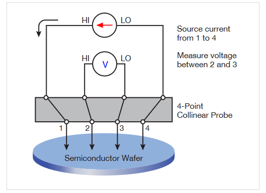
The two outer probes are used for sourcing current and the two inner probes are used for measuring the resulting voltage drop across the surface of the sample. The volume resistivity is calculated as follows:
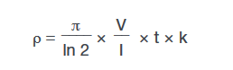
where: ρ = volume resistivity (Ω-cm)
V = the measured voltage (volts)
I = the source current (amperes)
t = the sample thickness (cm)
k* = a correction factor based on the ratio of the probe to wafer diameter and on the ratio of wafer thickness to probe separation
* The correction factors can be found in standard four-point probe resistivity test procedures such as SEMI MF84-02—Test Method for Measuring Resistivity of Silicon Wafers with an In-Line FourPoint Probe.
For some materials such as thin films and coatings, the sheet resistance, or surface resistivity, is determined instead, which does not take the thickness into account. The sheet resistance (σ) is calculated as follows:
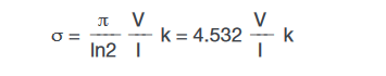
where: σ = the sheet resistance (Ω/square or just Ω)
Note that the units for sheet resistance are expressed in terms of Ω/square in order to distinguish this number from the measured resistance (V/I).
Using the Kelvin Technique to Eliminate Lead and Contact Resistance
Using four probes eliminates measurement errors due to the probe resistance, the spreading resistance under each probe, and the contact resistance between each metal probe and the semiconductor material. Figure 2 is another representation of the four-point collinear probe setup that shows some of the circuit resistances.
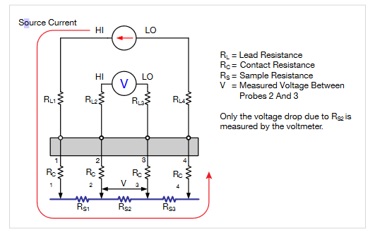
The RL terms represent the test lead resistance. RC represents the contact resistance between the metal probe and the semiconductor material. The contact resistance can be several hundred to a thousand times higher than the resistance of the sample material, which is represented by RS
Notice that the current flows through all the resistances in the first and fourth set of leads and probes, as well as through the semiconductor material. However, the voltage is only measured between probes 2 and 3. Given that between probes 2 and 3, the current only flows through RS2, only the voltage drop due to RS2will be measured by the voltmeter. All the other unwanted lead (RL) and contact (RC) resistances will not be measured.
Using the 4200A-SCS to Make Four-Point Probe Collinear Probe Measurements
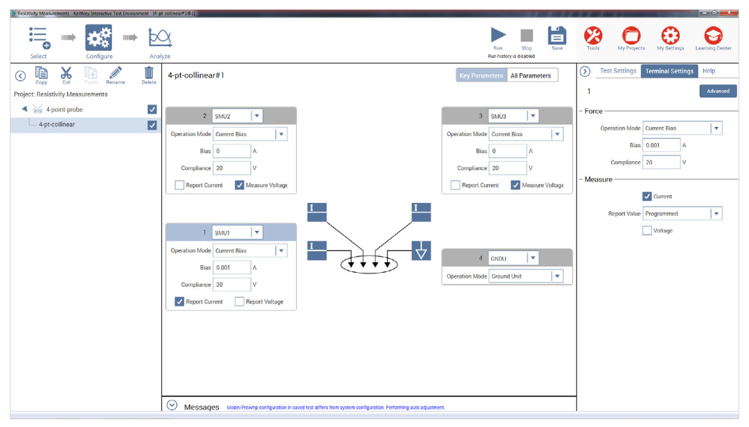
The 4200A-SCS comes with a project that is already configured for automating four-point probe resistivity measurements. The project, Four-Point Probe Resistivity Project, can be found in the Project Library in the Select view by selecting the Materials filter. This project has two tests: one measures the resistivity using a single test current and the other measures the resistivity as a function of a current sweep. These two tests, Four-Point Probe Resistivity Measurement (4-pt-collinear) and Four-Point Probe Resistivity Sweep (4-pt-resistivity-sweep), can also be found in the Test Library and can be added to a project. A screen capture of the Four-Point Probe Resistivity Measurement test is shown in Figure 3.
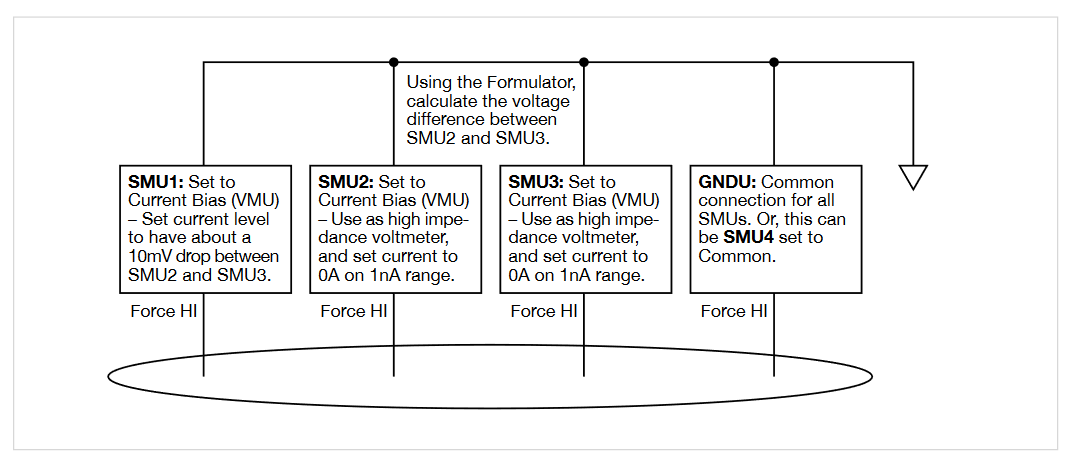
The projects and tests included with the 4200A-SCS are configured to use either three or four SMUs (Source Measure Units). When using three SMUs, all three SMUs are set to Current Bias (voltmeter mode). However, one SMU will source current (pin 1 of probe) and the other two (pins 2 and 3 of probe) will be used to measure the voltage difference between the two inner probes. An example of how this is set up with the 4200A-SCS is shown in Figure 4. One SMU (SMU1) and the GNDU (ground unit) are used to source current between the outer two probes. The other SMUs (SMU2 and SMU3) are used to measure the voltage drop between the two inner probes.
When configuring the tests, enter an appropriate test current for SMU1. This will depend on the resistivity of the sample. For higher resistance samples, additional Interval time may need to be added in the Test Settings pane to ensure a settled reading.
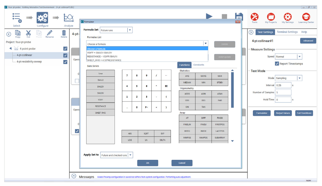
The Formulator in the Test Settings pane includes equations to derive the resistivity as shown in Figure 5. The voltage difference between SMU2 and SMU3 is calculated: VDIFF=SMU2V-SMU3V. The sheet resistivity (ohms/square) is derived from SMU1 current and voltage difference calculation, SHEET_RHO=4.532*(VDIFF/SMU1I). To determine the volume resistivity (ohms-cm), multiply the sheet resistivity by the thickness of the sample in centimeters (cm). If necessary, a correction factor can also be applied to the formula.
After the test is configured, lower the probe head so the pins are in contact with the sample. Execute the test by selecting Run at the top of the screen. The resistivity measurements will appear in the Sheet in the Analyze view.
Sources of Error and Measurement Considerations
For successful resistivity measurements, potential sources of errors need to be considered.
Electrostatic Interference
Electrostatic interference occurs when an electrically charged object is brought near an uncharged object. Usually, the effects of the interference are not noticeable because the charge dissipates rapidly at low resistance levels. However, high resistance materials do not allow the charge to decay quickly and unstable measurements may result. The erroneous readings may be due to either DC or AC electrostatic fields.
To minimize the effects of these fields, an electrostatic shield can be built to enclose the sensitive circuitry. The shield is made from a conductive material and is always connected to the low impedance (FORCE LO) terminal of the SMU instrument.
The cabling in the circuit must also be shielded. Low noise shielded triax cables are supplied with the 4200A-SCS.
Leakage Current
For high resistance samples, leakage current may degrade measurements. The leakage current is due to the insulation resistance of the cables, probes, and test fixturing. Leakage current may be minimized by using good quality insulators, by reducing humidity, and by using guarding.
A guard is a conductor connected to a low impedance point in the circuit that is nearly at the same potential as the high impedance lead being guarded. The inner shield of the triax connector of the 4200A-SCS is the guard terminal. This guard should be run from the 4200A-SCS to as close as possible to the sample. Using triax cabling and fixturing will ensure that the high impedance terminal of the sample is guarded. The guard connection will also reduce measurement time since the cable capacitance will no longer affect the time constant of the measurement.
Light
Currents generated by photoconductive effects can degrade measurements, especially on high resistance samples. To prevent this, the sample should be placed in a dark chamber.
Temperature
Thermoelectric voltages may also affect measurement accuracy. Temperature gradients may result if the sample temperature is not uniform. Thermoelectric voltages may also be generated from sample heating caused by the source current. Heating from the source current will more likely affect low resistance samples, because a higher test current is needed to make the voltage measurements easier. Temperature fluctuations in the laboratory environment may also affect measurements. Because semiconductors have a relatively large temperature coefficient, temperature variations in the laboratory may need to be compensated for by using correction factors.
Carrier Injection
To prevent minority/majority carrier injection from influencing resistivity measurements, the voltage difference between the two voltage sensing terminals should be kept at less than 100mV, ideally 25mV, since the thermal voltage, kt/q, is approximately 26mV. The test current should be kept as low as possible without affecting the measurement precision.
Conclusion
The 4200A-SCS Parameter Analyzer is an ideal tool for measuring resistivity of semiconductor materials using a fourpoint collinear probe. The built-in resistivity project and tests are configurable and include the necessary calculations.
van der Pauw and Hall Voltage Measurements with the 4200A-SCS Parameter Analyzer
Introduction
Semiconductor material research and device testing often involve determining the resistivity and Hall mobility of a sample. The resistivity of semiconductor material is primarily dependent on the bulk doping. In a device, the resistivity can affect the capacitance, the series resistance, and the threshold voltage.
The resistivity of the semiconductor material is often determined using a four-point probe technique. With a fourprobe, or Kelvin, technique, two of the probes are used to source current and the other two probes are used to measure voltage. Using four probes eliminates measurement errors due to the probe resistance, the spreading resistance under each probe, and the contact resistance between each metal probe and the semiconductor material. Because a high impedance voltmeter draws little current, the voltage drops across the probe resistance, spreading resistance, and contact resistance are very small.
One common Kelvin technique for determining the resistivity of a semiconductor material is the van der Pauw (VDP) method. The 4200A-SCS Parameter Analyzer includes a project for making van der Pauw measurements. Because of its high input impedance (>1016Ω) and accurate low current sourcing, the 4200A-SCS with preamps is ideal for high resistance samples. This application note explains how to make resistivity measurements of semiconductor materials using the 4200A-SCS and the van der Pauw method.
van der Pauw Resistivity Measurement Method
The van der Pauw method involves applying a current and measuring voltage using four small contacts on the circumference of a flat, arbitrarily shaped sample of uniform thickness. This method is particularly useful for measuring very small samples because geometric spacing of the contacts is unimportant. Effects due to a sample’s size, which is the approximate probe spacing, are irrelevant.
Using this method, the resistivity can be derived from a total of eight measurements that are made around the periphery of the sample with the configurations shown in Figure 1.
Once all the voltage measurements are taken, two values of resistivity, ρA and ρB, are derived as follows:
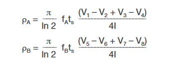
where: ρA and ρB are volume resistivities in ohm-cm;
ts is the sample thickness in cm;
V1–V8 represents the voltages measured by the voltmeter;
I is the current through the sample in amperes;
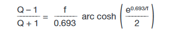
fA and fB are geometrical factors based on sample symmetry. They are related to the two resistance ratios QA and QB as shown in the following equations (fA = fB = 1 for perfect symmetry).
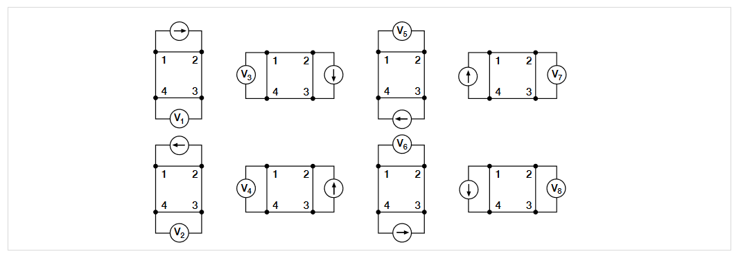
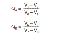
QA and QB are calculated using the measured voltages as follows:
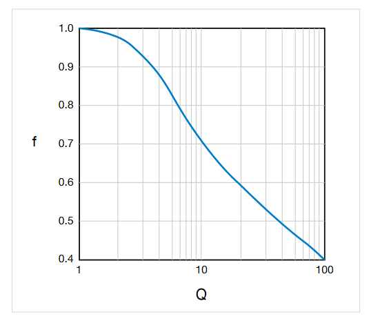
Also, Q and f are related as follows:
A plot of this function is shown in Figure 2. The value of f can be found from this plot once Q has been calculated.
Once ρA and ρB are known, the average resistivity (ρAVG) can be determined as follows:

Test Equipment
The electrical measurements for determining van der Pauw resistivity require a current source and a voltmeter. To automate measurements, one might typically use a programmable switch to switch the current source and the voltmeter to all sides of the sample. However, the 4200A-SCS is more efficient than this.
The 4200A-SCS with four SMU instruments and four preamps (for high resistance measurements) is an ideal solution for measuring van der Pauw resistivity, and should enable measurements of resistances greater than 1012Ω. Since each SMU instrument can be configured as a current source or as a voltmeter, no external switching is required, thus eliminating leakage and offsets errors caused by mechanical switches. This removes the need for additional instruments and programming.
For high resistance materials, a current source that can output very small current with a high output impedance is necessary. A differential electrometer with high input impedance is required to minimize loading effects on the sample. On the lowest current source ranges (1pA and 10pA) of the 4200A-SCS, the input resistance of the voltmeter is >1016Ω.
Using the 4200A-SCS to Measure Resistivity with the van der Pauw Method
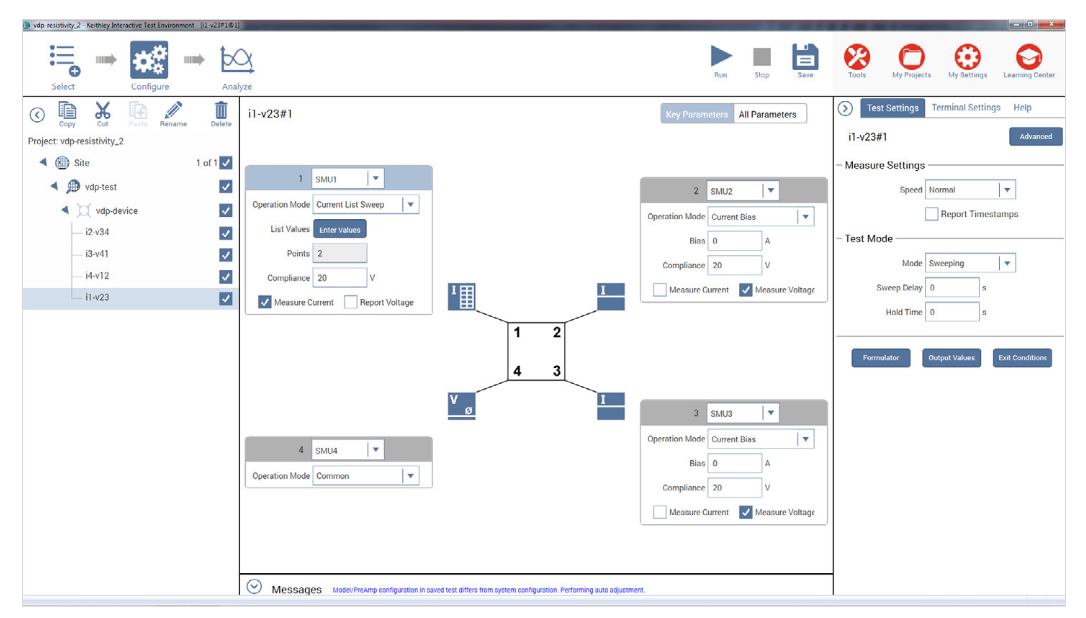
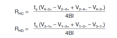
Each terminal of the sample is connected to one SMU instrument, so a 4200A-SCS with four SMU instruments is required. The van der Pauw Project, which has four tests, is in the Projects Library and can be found by selecting the Materials box from the Select pane. A screen capture of the van der Pauw project is shown in Figure 3.
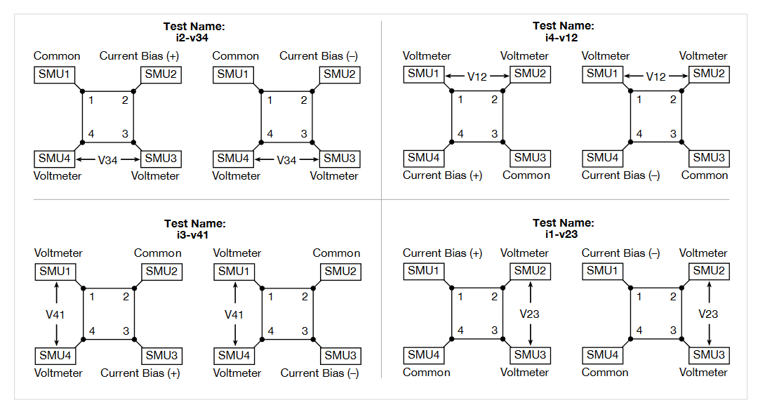
Each test has a different measurement setup. A diagram of how the four SMU instruments are configured in the four tests is shown in Figure 4. For each test, three of the SMU instruments are configured as a current bias and a voltmeter (VMU). One of these SMU instruments applies the test current and the other two SMU instruments are used as high impedance voltmeters with a test current of zero amps on a low current range (typically 1nA range). The fourth SMU instrument is set to common. The voltage difference is calculated between the two SMU instruments set up as high impedance voltmeters. This measurement setup is duplicated around the sample, with each of the four SMU instruments changing functions in each of the four tests. The test current and voltage differences between the terminals from the four tests are used to calculate the resistivity in the subsite calc sheet
Test Configurations for Measuring van der Pauw Resistivity
In each of the four tests, one SMU instrument is configured as the current source using the current list sweep function, two SMU instruments are configured as voltmeters, and one is configured as a common. Here is the configuration for the i1-v23 test:
Terminal 1 – SMU1: Set to a two-point Current List Sweep. Enter both the positive and negative values of the appropriate source current. Enter the Compliance level and use the Best Fixed source range. Averaging voltage measurements (from SMU2 and SMU3) taken at both a positive and negative test current will correct for voltage offsets in the circuit.
Terminal 2 – SMU2: Set to Current Bias (VMU) with a test current of 0A. Set the appropriate compliance voltage, and check the Measure Voltage box (VB). Even though 0A will be output, select an appropriate current source range. The input impedance of the voltmeter is directly related to the current source range. The lower the current source range is, the higher the input impedance will be. However, the lower the current source range, the slower the measurement time will be. For most applications, the 1nA range may be used. However, for very high resistance measurements, use a lower current range
Terminal 3 – SMU3: Set up the same as Terminal B.
Terminal 4 – SMU4: Set the Operation Mode to Common.
In this test, the current is sourced between Terminals 1 and 4 (SMU1 to SMU4). SMU2 will measure the voltage from Terminal 2 to Terminal 4. SMU3 will measure the voltage from Terminal 3 to Terminal 4.
The Formulator calculates the voltage difference between SMU2 and SMU3 for both the positive and negative test current. This can be done using an equation such as V23DIFF=V2-V3. The absolute values of these numbers (from both the positive and negative test current) are taken using the ABS function with an equation such as V23ABS=ABS(V23DIFF). The two voltage difference values are averaged using the AVG function with an equation, such as V23=AVG(ABSV23). In the Output Values dialog box located on the Test Settings pane, the average voltage (V23) is selected so that it is sent to the subsite data sheet, where it will be used in the resistivity calculation. The magnitude of the current source must also be sent to the subsite data sheet, so click that check box (I1) as well.
This same procedure is repeated in all four tests so that all sides of the sample are measured, as shown previously in Figure 1. The average voltages from each test are then used to calculate the resistivity on the subsite Calc sheet. A diagram showing how the SMUs are set up in each test is shown in Figure 4.
Adjusting the Source Current
The source current value will need to be modified according to the expected sample resistance. Adjust the current so that the voltage difference will not exceed 25mV (approximately).In each of the four tests (i2-v34, i3-v41, i4-v12, i1-v23), enter both polarities of the test current. The same magnitude must be used for each test.
Determining the Settling Time
For high resistance samples, it will be necessary to determine the settling time of the measurement. This can be accomplished by sourcing current into two terminals of the sample and measuring the voltage difference between the other two terminals. The settling time can be determined by graphing the voltage difference versus the time of the measurement.
Using the 4200A-SCS, the voltage versus time graph can easily be created by copying and pasting one of the tests described previously. In the Test Settings pane, take a few hundred or so readings with a sweep time of one second. Make sure that the Timestamp box is selected. After the readings are done, plot the voltage difference versus time on the graph. (You can choose the parameters to graph by using Graph Settings.) The settling time is determined from the graph. A timing graph of a very high resistance material is shown in Figure 5.
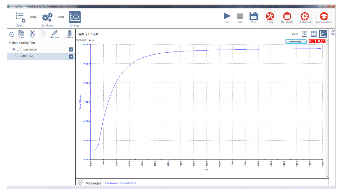
Determine the settling time by visually inspecting the voltage difference vs. time graph. Once the settling time has been determined, use this time as the Sweep Delay (in the Test Settings pane) for the four resistivity measurement tests listed previously. This settling time procedure will need to be repeated for different materials; however, it is not necessary for low resistance materials since they have a short settling time.
Calculating the Resistivity
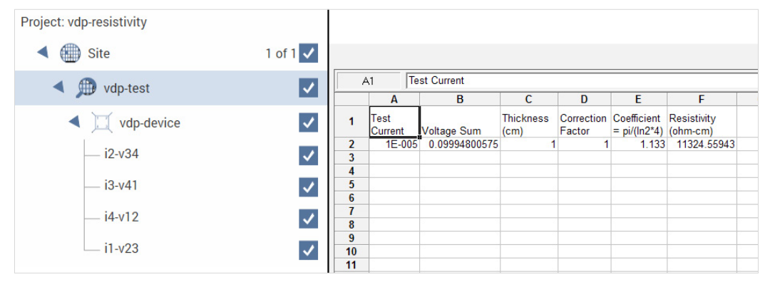
To view the calculated resistivity in the subsite level, select the subsite plan in the Project Tree. The Output Values (voltage differences and test current) will appear on the data sheet at the subsite level. The resistivity is calculated on the Calc sheet from the cell references on the Data sheet. The thickness, coefficients, and correction factors are also input on the Calc sheet for the resistivity equation.
These values can be updated in the Calc sheet in the subsite level. Select the subsite “vdp-test.” Go to the Subsite Data tab. It contains the output values of the voltage differences and the test current. From the Calc Sheet tab, the thickness can be adjusted. The default thickness is 1cm. If necessary, a correction factor can also be applied to the resistivity equation.
Running the Project
The van der Pauw Project (vdp-resistivity) must be run at the subsite level. Make sure that all boxes in the Project are checked and select the vdp-test subsite. Execute the project by using the Run button. Each time the test is run, the subsite data is updated. The voltage differences from each of the four tests (i2-v34, i3-v41, i4-v12, i1-v23) will appear in the Subsite Data “vdp-device” sheet. The resistivity will appear in the Subsite Data “Calc” sheet as shown in Figure 6.
Hall Voltage Measurements
Hall effect measurements are important to semiconductor material characterization because from the Hall voltage, the conductivity type, carrier density, and mobility can be derived. With an applied magnetic field, the Hall voltage can be measured using the configurations shown in Figure 7.
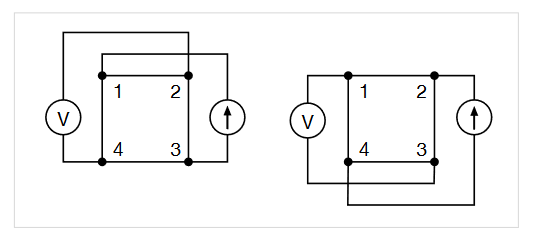
With a positive magnetic field, B, apply a current between terminals 1 and 3, and measure the voltage drop (V2–4+) between terminals 2 and 4. Reverse the current and measure the voltage drop (V4–2+). Next, apply current between terminals 2 and 4, and measure the voltage drop (V1–3+) between terminals 1 and 3. Reverse the current and measure the voltage (V3–1+) again.
Reverse the magnetic field, B, and repeat the procedure again, measuring the four voltages: (V2–4–), (V4–2–), (V1–3–), and (V3–1–).
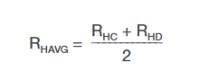
From the eight Hall voltage measurements, the average Hall coefficient can be calculated as follows:
where: RHC and RHD are Hall coefficients in cm3/C;
ts is the sample thickness in cm;
V represents the voltages measured by the voltmeter;
I is the current through the sample in amperes;
B is the magnetic flux in Vs/cm2 (1 Vs/cm2 = 108 gauss)
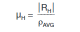
Once RHC and RHD have been calculated, the average Hall coefficient (RHAVG) can be determined as follows:
From the resistivity (ρAVG) and the Hall coefficient (RHAVG), the mobility (μH) can be calculated:
Using the 4200A-SCS to Measure the Hall Voltage
The setup to measure the Hall voltage is very similar to the setup for measuring resistivity. The difference is the location of the current source and voltmeter terminals. Figure 7 illustrates the setup for Hall voltage measurements. (Figure 4 illustrates the setup for resistivity measurements.) If the usersupplied electromagnet has an IEEE-488 interface, a program can be written in KULT (Keithley User Library Tool) to control the electromagnet using the 4200A-SCS. This would require that the 4200A-SCS have the 4200-COMPILER option.
Sources of Error and Measurement Considerations
For successful resistivity measurements, the potential sources of errors need to be considered.
Electrostatic Interference
Electrostatic interference occurs when an electrically charged object is brought near an uncharged object. Usually, the effects of the interference are not noticeable because the charge dissipates rapidly at low resistance levels. However, high resistance materials do not allow the charge to decay quickly and unstable measurements may result. The erroneous readings may be due to either DC or AC electrostatic fields.
To minimize the effects of these fields, an electrostatic shield can be built to enclose the sensitive circuitry. The shield is made from a conductive material and is always connected to the low impedance (FORCE LO) terminal of the SMU instrument.
The cabling in the circuit must also be shielded. Low noise shielded triax cables are supplied with the 4200A-SCS.
Leakage Current
For high resistance samples, leakage current may degrade measurements. The leakage current is due to the insulation resistance of the cables, probes, and test fixturing. Leakage current may be minimized by using good quality insulators, by reducing humidity, and by using guarding.
A guard is a conductor connected to a low impedance point in the circuit that is nearly at the same potential as the high impedance lead being guarded. The inner shield of the triax connector of the 4200-SMU is the guard terminal. This guard should be run from the 4200-SMU to as close as possible to the sample. Using triax cabling and fixturing will ensure that the high impedance terminal of the sample is guarded. The guard connection will also reduce measurement time since the cable capacitance will no longer affect the time constant of the measurement.
Light
Currents generated by photoconductive effects can degrade measurements, especially on high resistance samples. To prevent this, the sample should be placed in a dark chamber
Temperature
Thermoelectric voltages may also affect measurement accuracy. Temperature gradients may result if the sample temperature is not uniform. Thermoelectric voltages may also be generated from sample heating caused by the source current. Heating from the source current will more likely affect low resistance samples because a higher test current is needed to make the voltage measurements easier. Temperature fluctuations in the laboratory environment may also affect measurements. Since semiconductors have a relatively large temperature coefficient, temperature variations in the laboratory may need to be compensated for by using correction factors.
Carrier Injection
To prevent minority/majority carrier injection from influencing resistivity measurements, the voltage difference between the two voltage sensing terminals should be kept at less than 100mV, ideally 25mV, given that the thermal voltage, kt/q, is approximately 26mV. The test current should be kept to as low as possible without affecting the measurement precision.