1 Introduction
This MOI specifies the testing procedures for the Super Speed channels of a USB 3.0 cable and mated cable assembly. In particular, it verifies the following characteristics for compliance to the “Universal Serial Bus 3.0 Connectors and Cable Assemblies Compliance Document”1. Verification of the High Speed channel (D+ and D-) may be done according to the USB 2 Cable Test MOI.
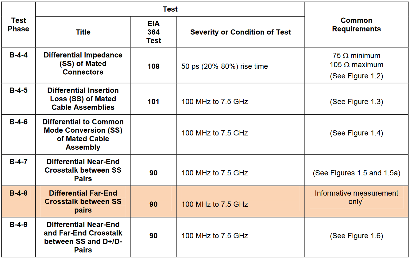
Test Group B-4: High Speed Testing
1.1 Instrumentation Requirements
1.1.1 Best Configuration
DSA8200 mainframe or equivalent3.
Two 80E08 or 80E10
IConnect software (80SSPAR, 80SICON or 80SICMX) version 5.0 or later (w/ S-Parameter Wizard)
One set of Approved USB 3.0 test fixtures
4 equal (~ 6 in) length SMA cables 20GHz bandwidth or equivalent4
2 SMA male to male adaptors.
50 Ohm terminations to terminate unused channels
1.1.2 Good Configuration
DSA8200 mainframe or equivalent1.
Two 80E045
IConnect software (80SSPAR, 80SICON, or 80SICMX) version 5.0 or later (w/ S-Parameter Wizard)
One set of USB 3.0 test fixtures
4 pcs. equal length (~18 in) SMA cables 20GHz bandwidth or equivalent6
2 pcs. SMA Female to Female adaptors.
50 Ohm terminations to terminate unused channels
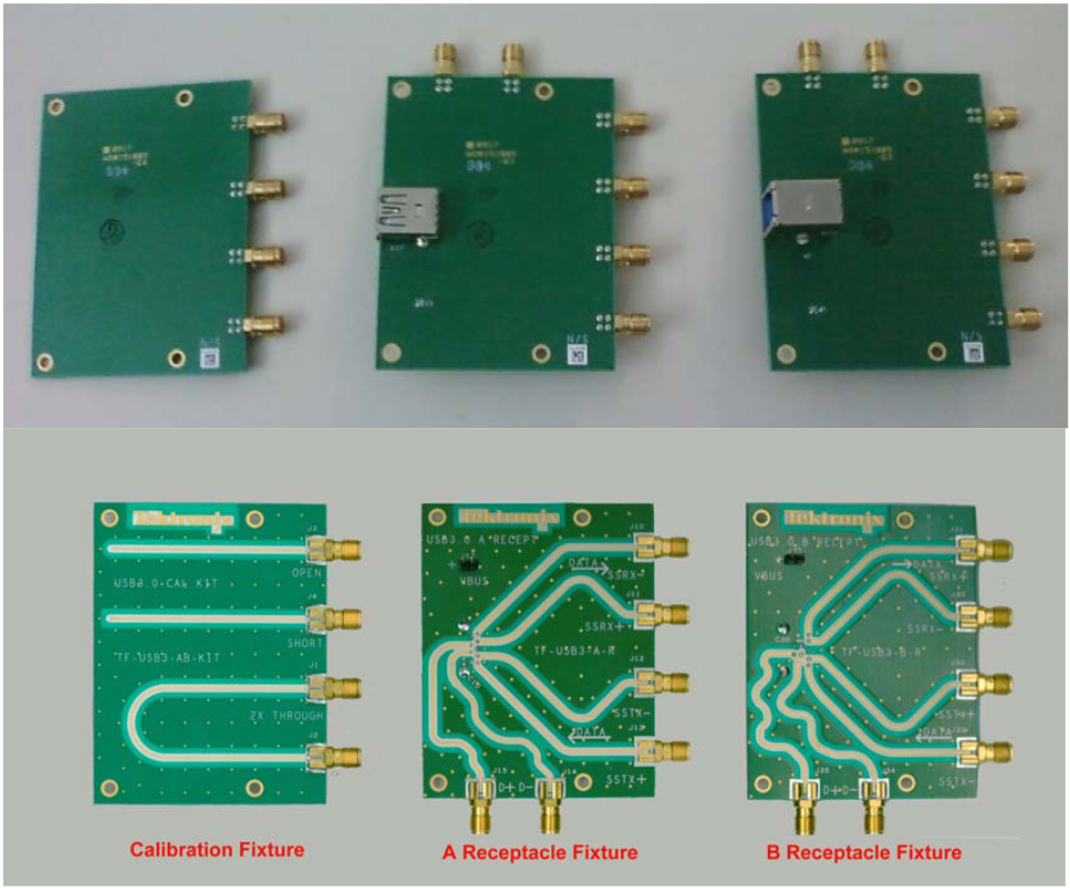
1.1.3 USB 3.0 Test Fixtures
In order to make accurate, repeatable measurements for USB 3.0 cable compliance testing it is critical that one use a set of high quality test fixtures. These will include (as a minimum):
- “A-Receptacle” test fixture
- “B-Receptacle” test fixture
- Calibration test fixture(s)
In addition, if one is also testing USB 3 cable with stacked A connectors or micro plugs, one must have test fixtures that accommodate those form factors as well.
High quality test fixtures have equal length traces for all signals from the test point connectors to the plug receptacles (typically controlled to < 1psec). In addition, the impedance of these traces should be well matched to <7% variance.
Shown below is Tektronix’ USB 3.0 cable test fixtures. All diagrams as well as test fixture specific procedures in this MOI are based on these fixtures. Other test fixtures may be used in lieu of these. For information on these other fixtures and deviations of the test methodology when using these fixtures, see the Appendices.
1.1.4 Test Setup Diagrams
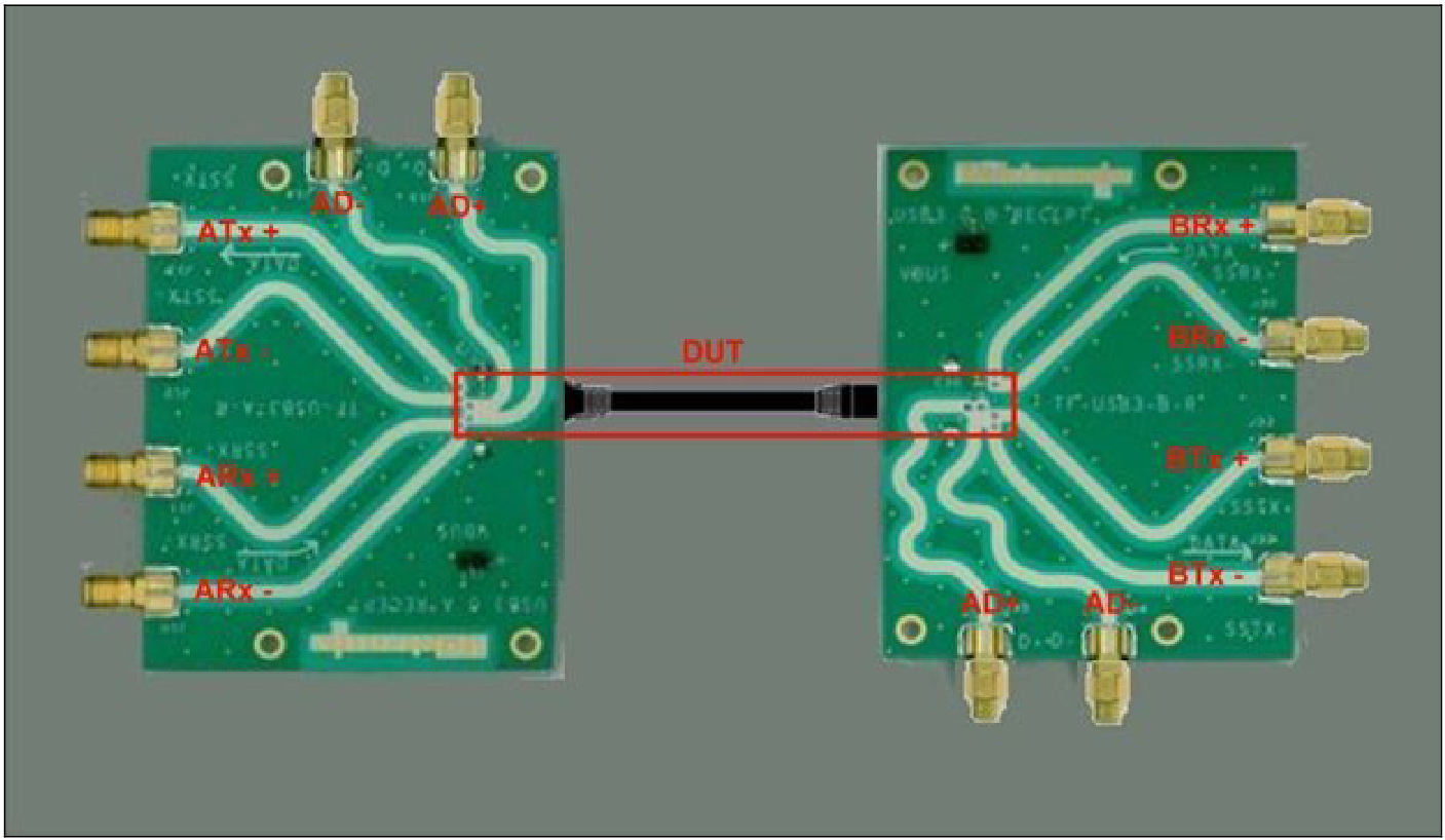
For most of the test setup diagrams in this document, the fixtures are shown with the back side up, the A-Receptacle at the left and the B-Receptacle at the right as shown in figure 1.4, below.
1.1.5 IConnect Limit Test Files
The test procedures in this MOI utilize IConnect to verify the performance of the cables being tested against limits specified by the “Universal Serial Bus 3.0 Connectors and Cable Assemblies Compliance Document”. These limits are encoded in a number of IConnect files which are distributed with this document. The complete list of these files is shown below:
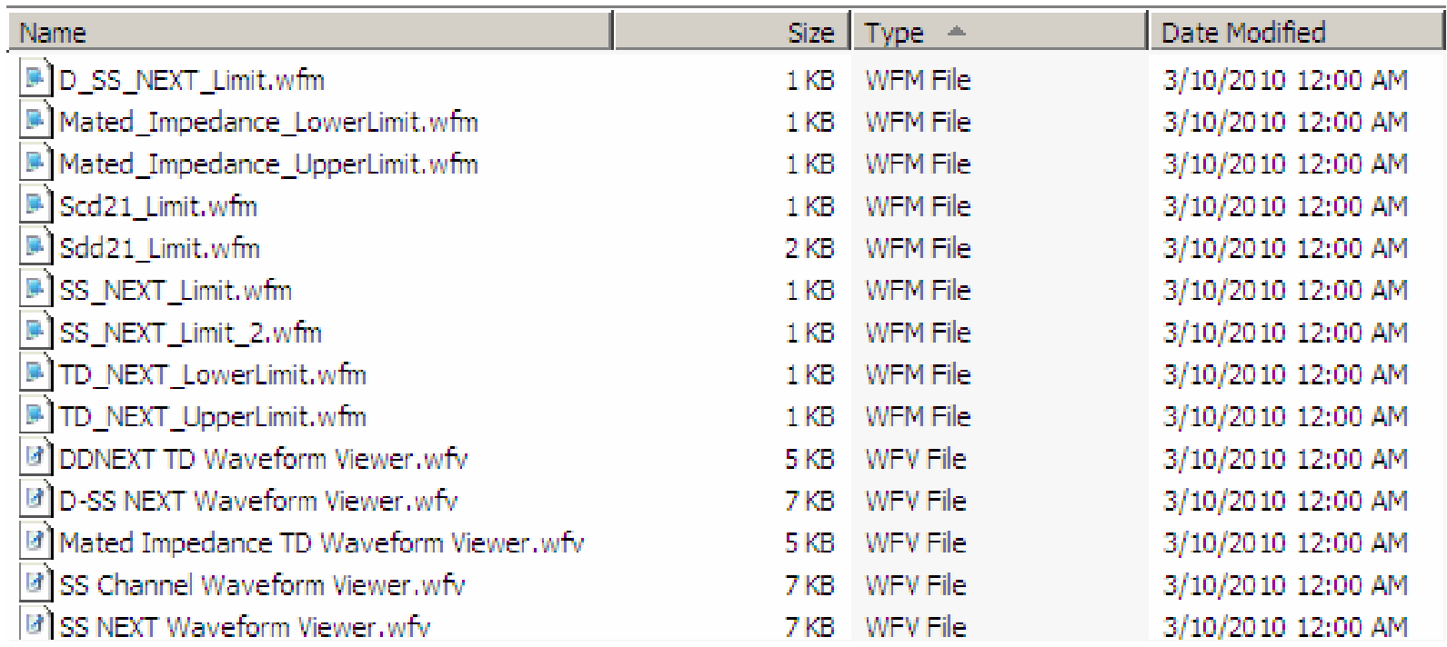
These files should be copied into a single directory for loading into IConnect in the Limit Test sections of this test procedure.
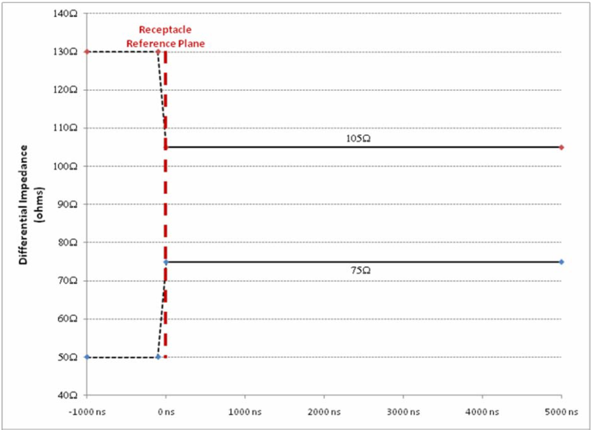
1.2 Differential Impedance (SS) of Mated Connectors
For this test, one must establish the reference plane for the plug receptacle and apply a 50 psec (20-80%) rise time step and measure the impedance of the mated connector ensuring that it falls within the limits (75 - 105) as shown in figure 1.2, below.
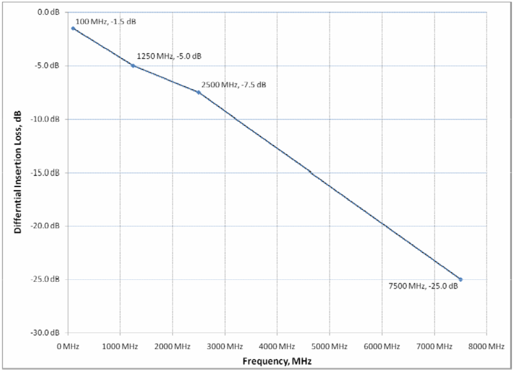
1.3 Differential Insertion Loss (SS) of Mated Cable Assemblies
For this test, one measures the insertion loss (Sdd21) for each of the SS channels and verifies that the insertion loss is less than the limit shown in figure 1.3, below. (The limit shown is a lower limit – i.e. the insertion loss should fall above the limit line shown.)
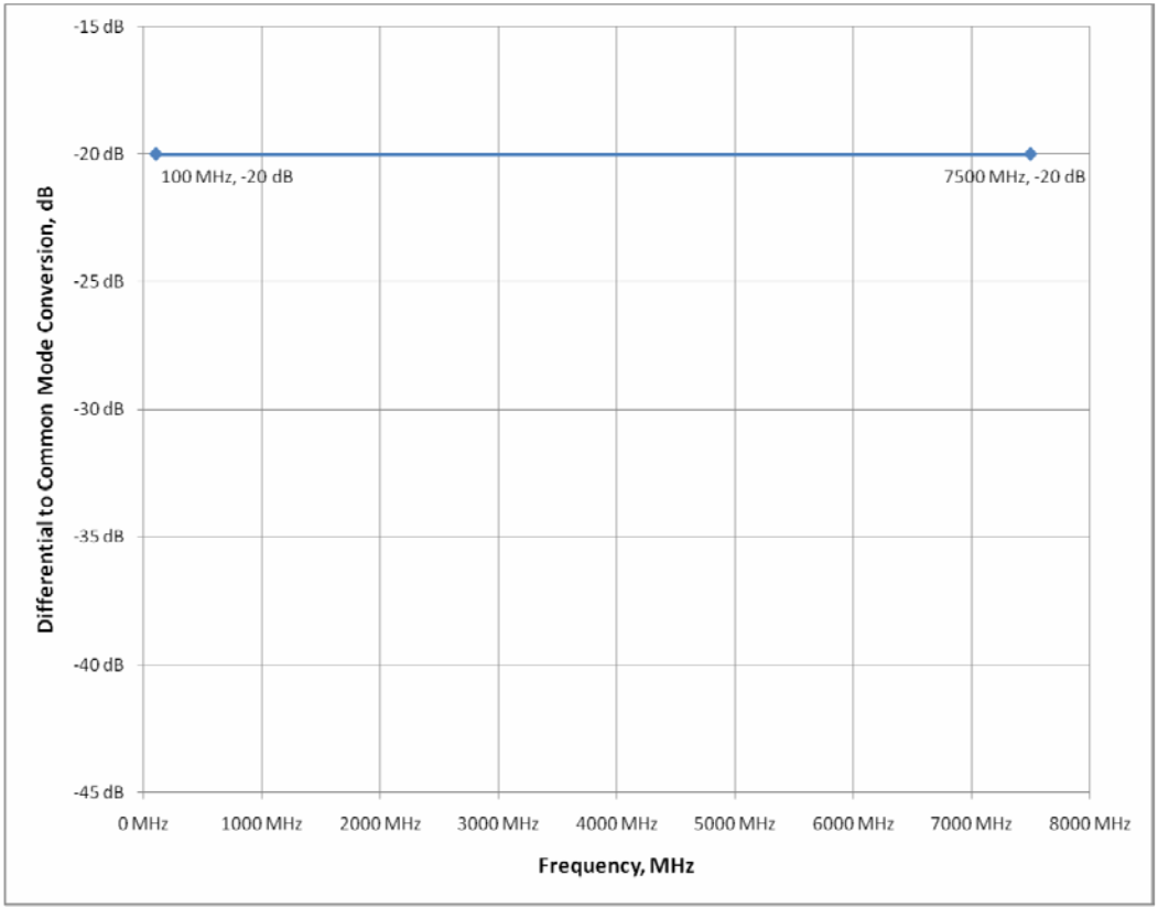
1.4 Differential to Common Mode Conversion (SS) of Mated Cable Assembly
For this test, one measures the common mode conversion (Scd21) for each of the SS channels and verifies that the common mode conversion is less than the limit shown in figure 1.4, below. (The limit shown is an upper limit – i.e. the common mode conversion should fall below the limit line shown.)
1.5 Differential Near-End Crosstalk (DDNEXT) between Super Speed Pairs
For this test, one measures the differential near-end crosstalk (DDNEXT) between the SS channels at both the A- and B-receptacles. This cross-talk is then compared to the limits shown in figure 1.5a, below. (These limits are upper limits – i.e. the crosstalk should fall below the limit line(s) shown.)
If the crosstalk is less than the lower limit (-32dB from 100 to 2500 MHz), no further testing is required. If the crosstalk is greater than the upper limit (-27dB from 100 to 2500 MHz) the crosstalk test is deemed to have failed.
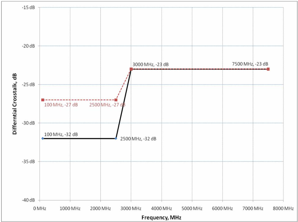
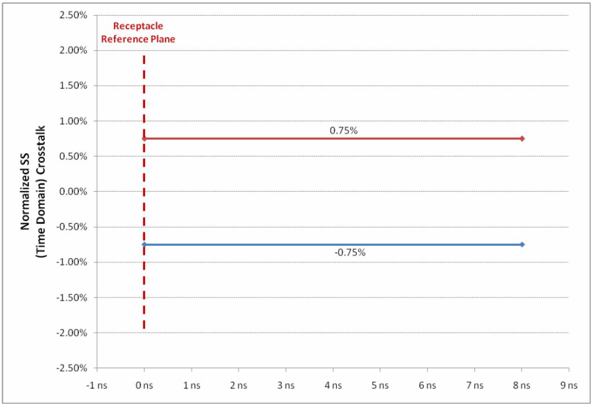
If the measured crosstalk fails the lower limit but passes the upper limit, one must look at the crosstalk in the time domain. For this test, one must establish the reference plane for the plug receptacle and apply a 50 psec (20-80%) rise time step and measure the crosstalk in the time domain ensuring that the peak to peak time domain crosstalk is less than 1.5% of the differential step amplitude as shown in figure 1.5b, below.
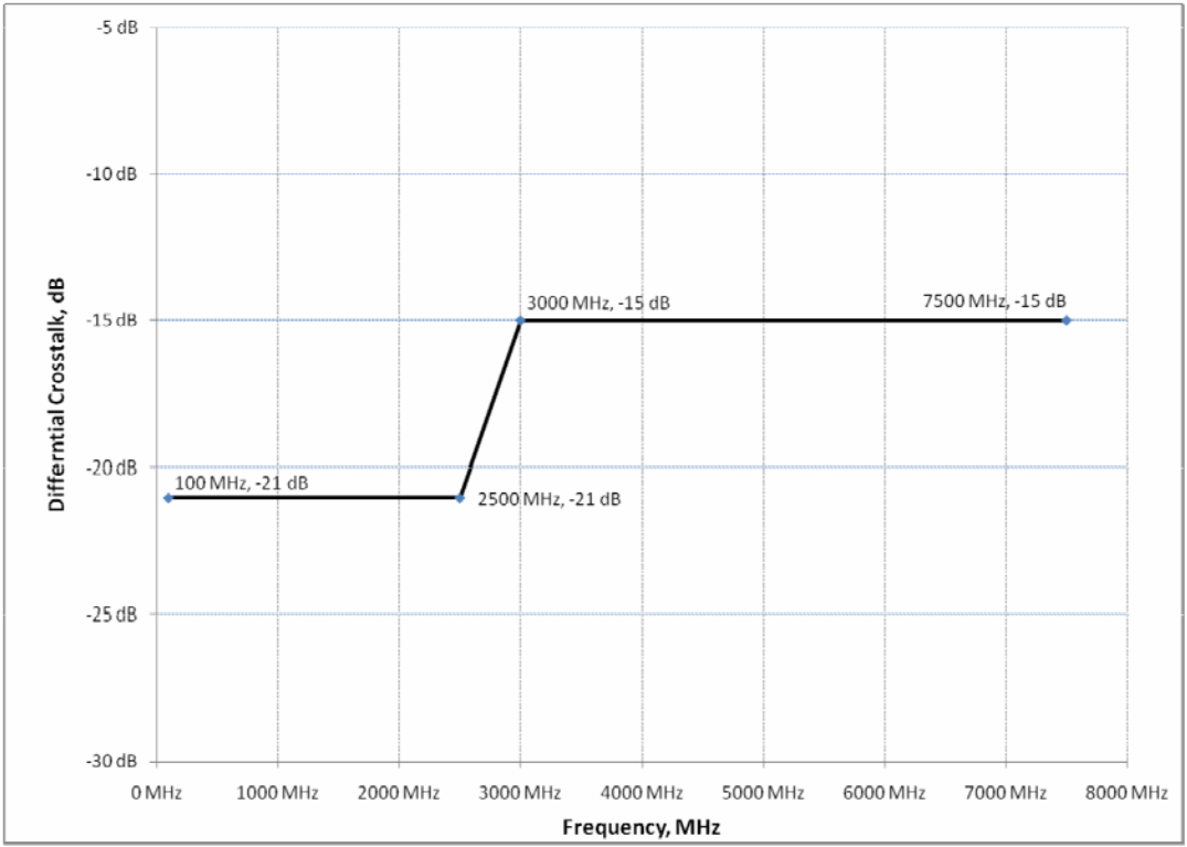
1.6 Differential Crosstalk (NEXT and FEXT) between Super Speed Channels and High Speed Channel (D+/D-)
For this test, one measures the differential near-end crosstalk (NEXT) and far-end crosstalk (FEXT) between the HS channel and the SS channels at both the A- and Breceptacles. This cross-talk is then compared to the limits shown in figure 1.6, below. (These limits are upper limits – i.e. the crosstalk should fall below the limit line shown.)
2 Outline of Testing
Following are the steps to execute for the USB 3.0 High Speed Electrical Cable Testing (detailed instructions for each step are in following sections).
- Setup the test system as follows:
- Perform compensation for all channels and the mainframe.
- Connect matched SMA cables to the sampling heads of the mainframe.
- Perform the differential acquisition and TDR deskew procedures for all channels at the SMA interface.
- Determine the appropriate rise time filter (to yield 50 psec 20-80 rise time) for time domain measurements.
- Save instrument setup for future additional cable measurements.
- Acquire differential timing reference waveform and setup the plug receptacle reference plane (nominally at 1 nsec) for impedance and time domain crosstalk measurement (if required).
- Configure the instrument and acquire normalized waveforms to measure the mated cable differential impedance for SS channels at both A and B receptacles and (using IConnect) compare the mated impedance against limits to verify in compliance with the standard.
- Configure the instrument and acquire waveforms to measure time domain differential near-end crosstalk (DDNEXT) for SS channels at both A and B receptacles and (using IConnect) compare time domain differential near-end crosstalk (DDNEXT) for SS channels against limits. (These measurement results are only required if the device under test fails DDNEXT in the frequency domain.)
- Using the IConnect® S-Parameter Wizard, acquire the following S-Parameter SubNetworks
- DUT1: A_Tx → B_Rx Insertion Loss
- DUT2: B_Tx → A_Rx Insertion Loss
- DUT3: B_DDNEXT (= B_Tx → B_Rx Insertion Loss)
- DUT4: A_DDNEXT (= A_Tx → A_Rx Insertion Loss)
- DUT5: D → A DDNEXT (= A_D → A_Rx Insertion Loss)
- DUT6: D → A DDFEXT (= B_D → A_Rx Insertion Loss)
- DUT7: D → B DDNEXT (= B_D → B_Rx Insertion Loss)
- DUT8: D → B DDFEXT (= A_D → B_Rx Insertion Loss)
- Using IConnect compare s-parameter waveforms against limits to verify compliance.
3 Detailed Test Procedures
3.1 Setup the Test System
In order to make accurate, repeatable measurements with the Tektronix DSA8200 Digital Serial Analyzer (or equivalent) one must ensure that the instrument has been properly configured, warmed up and compensation run on both the mainframe and the TDR modules that will be used to make the USB 3 cable measurements.
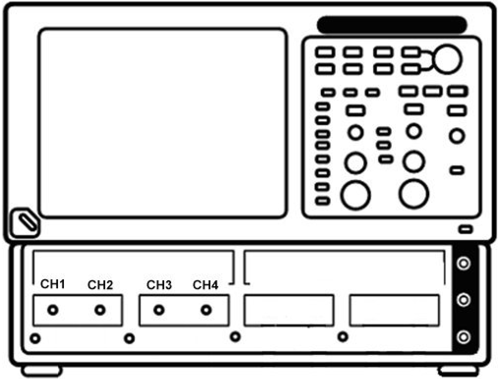
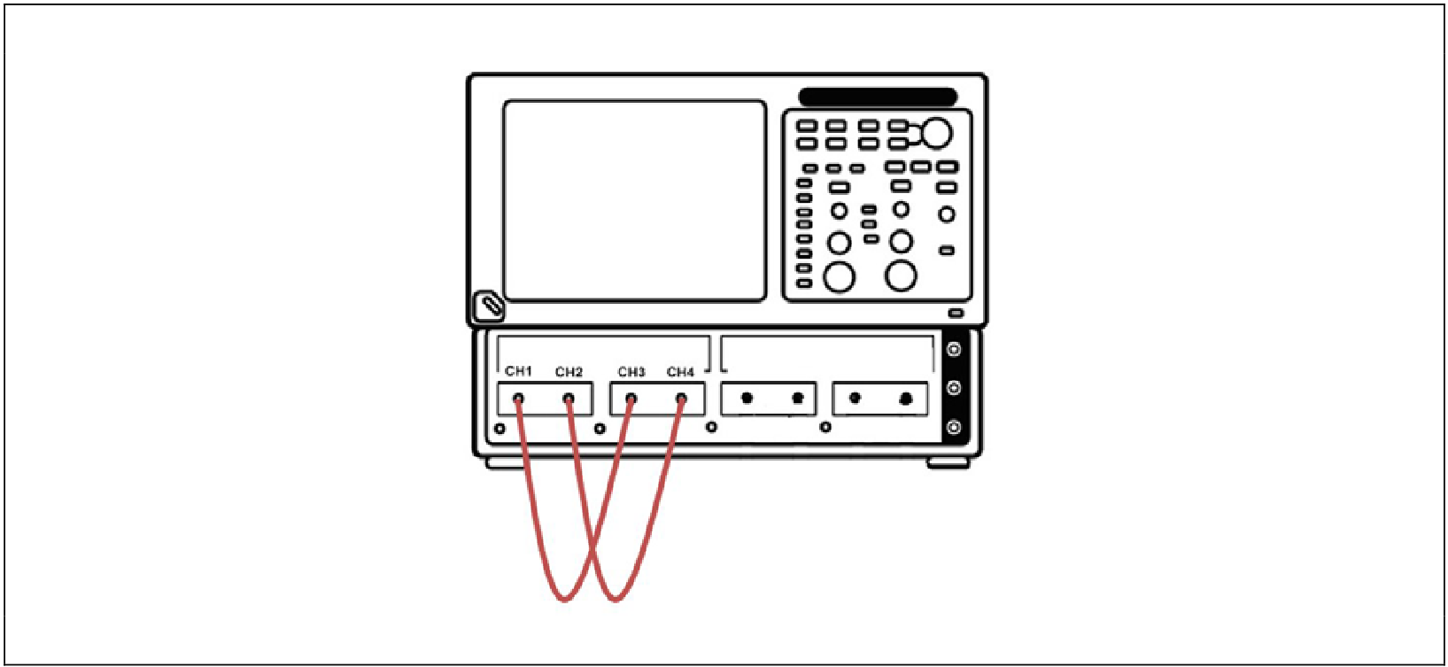
While the TDR modules can be installed in any of the four lower module slots of the DSA8200, the following procedures assume that they have been installed in the leftmost slots (Channels 1-4) of the mainframe (as represented in figure 3.1 below).
Once these modules have been installed, power on the instrument. The timing and vertical accuracy specifications for sampling oscilloscopes are temperature dependent and thus it is critical that the instrument be allowed to warm up to its steady state temperature. While the instrument may warm up more quickly, it is recommended that after powering on the instrument one wait 20 minutes to ensure temperature stabilization.
Since the accuracy of the instrument is temperature dependent, it is important that once the temperature has stabilized “compensation” be run for both the mainframe and the installed modules. More information on instrument compensation can be found in the instrument’s user documentation.
Note: Sampling modules are very sensitive to electro-static discharge (ESD) and electrical over-voltage stress (EOS); therefore one should use standard static protection procedures to avoid damaging the sampler inputs to these modules.
Having compensated the instrument, connect matched cables to the sampler outputs and proceed with the acquisition and step alignment. If you are using 80E10 50GHz TDR modules, it is necessary that you provide good quality V (1.85mm) to SMA adapters as the quality of the measurements you make could be adversely affected by inferior adapters.
3.1.1 Acquisiton Channel Alignment
Since the measurements made in this testing are on differential signals it is important to ensure that the stimulus and acquisition on all channels is well aligned.
Required Equipment
- One sampling oscilloscope mainframe (TDS8000, TDS/CSA/DSA8200).
- Two TDR sampling modules (80E04, 80E08, or 80E10);
- Four pairs of matched SMA cables
- One SMA barrel (female-to-female) adaptor.
This procedure is to adjust (deskew) the acquisition strobe on each channel so that the samplers measure the signal at the end of the SMA cables precisely at the same time. The strobe adjustment is compensating for cable and sampler differences.
In the first stage, channels 1, 2 and 3 acquisitions are aligned using channel 4 as the TDR source. In stage two, the acquisition strobe of channel 4 is aligned with channel 3 using channel 1 as the TDR step source. The deskew procedures are performed using the default TDR rho units.
Notes on two critical items:
- In order to cover the acquisition deskew range for some older instruments, it is required to start with a 1ns deskew value for all modules.
- Once a horizontal reference is established, DO NOT MOVE THE HORIZONTAL POSITION WHEN ALIGNING CHANNELS! Change only the Deskew values. Otherwise the acquisition deskew process needs to be restarted.
Follow the steps:
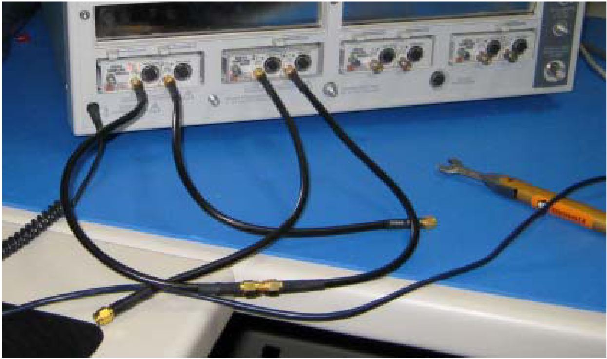
- Connect matched SMA cables to the sampling modules of the oscilloscope. For the best results, it is desired that the SMA cables used in the measurements have approximately the same quality and length, matched within 20ps.
- Set Deskew value (Vertical menu) for all 4 channels to 1ns to optimize the alignment range.
- Connect the SMA cables connected to channel 1 and channel 4 with an SMA barrel.
- Activate the TDR step on channel 4 and enable acquisition on channel 1 (see figure 3.1.1b). Use TDR Preset on C4 to setup the appropriate trigger and acquisition modes. Turn OFF acquisition on C4, acquisition will be done on C1.
- Set Record Length to 4000 points. Adjust the horizontal position and scale to get the rising edge on screen with good resolution (20ps/div).
- Save C1 waveform as a reference trace, R1. Channel 2 and 3 will be aligned with respect to it.
- Connect C2 to the C4 using SMA barrel, and display C2 on the screen.
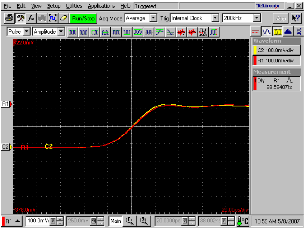
- Turn on the Delay measurement to measure the time difference between the rising edge on the reference trace, R1, and the rising edge of C2 as shown in figure 3.1.1c.
- Adjust the C2 Delay (For 80E04 use Deskew) value in the Vertical menu of the Setups dialog until a delay value within 1ps is achieved as shown in figure 3.1.1.c.
- Repeat steps 7-9 for the C3, so acquisition on channels C1 through C3 are aligned.
- Connect C3 to C1 using a SMA barrel.
- Activate TDR step on C1, acquire on C3, and save acquisition on C3 in R2.
- Repeat steps 7-9 for C4, using R2 as reference. DO NOT MOVE THE HORIZONTAL POSITION, but adjust the Delay (For 80E04 use Deskew) only! Change Delay measurement reference source to R2.
Generate a new reference for aligning acquisition on C4 with the rest of the channels, by using the TDR step of C1 as source, and the acquisition on C3 as the new reference.
Now all four acquisition channels have been de-skewed within 1ps.
3.1.2 TDR Step Alignment
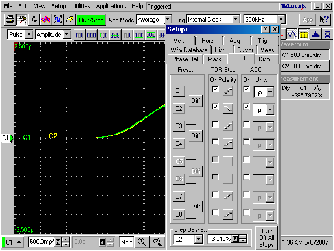
The purpose of this step is to adjust the TDR pulses so they arrive at the ends of the cables at precisely the same time. The deskew procedure is performed in rho mode. Disconnect all SMA barrels and follow the steps below:
- Turn on differential TDR mode for the first module, C1 and C2, using the TDR Differential Preset control.
- Adjust the horizontal position and scale so that the reflected open TDR steps are visible on screen with good resolution, 20ps/div. See Figure 3.1.2.
- Turn on the Delay measurement to measure the time difference between the two pulses acquired on C1 and C2.
- Select the C2 Step Deskew in the TDR menu and adjust its value to minimize the time difference between the C1 and C2 pulses as they reach the DUT. You need to activate the Fine button to improve the resolution of the adjustment.
- Repeat steps 1-4 for C3 and C4.
The instrument is set up now to make accurate differential mode TDR measurements.
SAVE THE INSTRUMENT SETTINGS IN ORDER TO BE ABLE TO RECALL THEM AT A LATER TIME, IF NECESSARY.
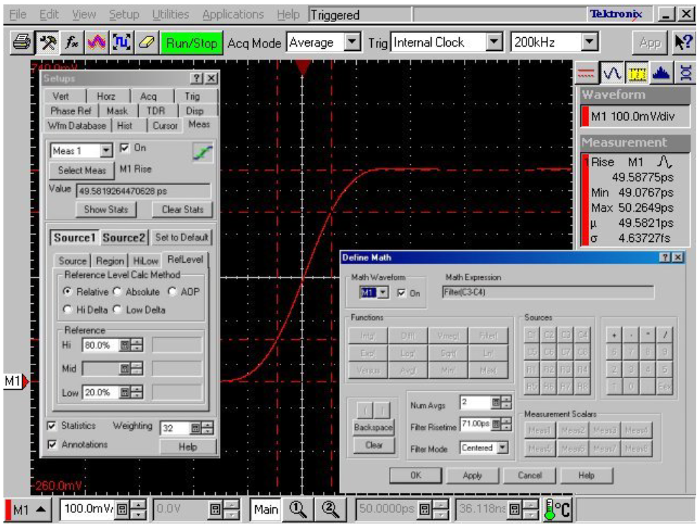
3.1.3 Determine Rise Time Filtering for Time Domain Measurements
The time domain measurements for USB 3.0 cable testing require that the DUT be stimulated with a 50 psec 20-80% rise time step. Since the rise time of various TD modules can vary (both as a normal function of process variation as well as differences in the designed rise time of different products), it is necessary to adjust the time domain measurements to compute them with the desired rise time. This is accomplished in the DSA8200 by applying a rise time filter to acquired waveforms.
The standard specifies that the rise time of the step should be measured at the reference plane of the DUT. Since there is very little loss in the short traces on the test fixtures, we will measure the required rise time filter value at the end of the SMA cables that will connect to the test fixtures as follows:
- Disconnect the SMA cables from C3 and C4.
MAKE SURE TO NOTE WHICH CABLE WAS ON WHICH CHANNEL AS YOU WILL WANT TO RECONNECT THEM IN ORDER TO MAINTAIN THE DESKEW THAT YOU DID IN SECTIONS 3.1.1 AND 3.1.2, ABOVE. - Connect the cable from C1 to C3 and C2 to C4, as shown in figure 3.1.3a, below.
- Press the “FINE” button on the front panel of the DSA8200 in order to be able to do fine adjustments to the rise time filter value.
- Turn on a differential TDR for C1 and C2 by pressing the Differential Preset button for these channels in the TDR setup dialog; turn off the acquisition and display of C1 and C2. The TDR units should be set to volts (V) for all 4 channels.
- Define math waveform 1 (M1) to be equal to “Filter(C3-C4)”, setting the filter value to 60 psec and turn it on using the Math Definition dialog (figure 3.1.3b)
- Set the acquisition record length for the Main Timebase to 4000 points (by turning the resolution knob on the front panel clockwise one full turn).
- Adjust the main time base scale to 50 psec / division and position M1 such that you can see the rising edge of this signal.
- Setup a pulse rise time measurement on M1 and set its High and Low Reference Levels to 80% and 20%, respectively.
- Returning to the Math Definition dialog for M1, adjust the filter rise time value using the up and down arrows until the measured rise time is 50 psec ± 0.5 psec.
RECORD THE REQUIRED FILTER RISE TIME VALUE AS THIS WILL BE NEEDED IN FUTURE MEASUREMENTS. - Reattach the SMA cables to C3 and C4. Turn off M1 and reset Meas1 to None.
3.2 Mated Cable Differential Impedance Tests
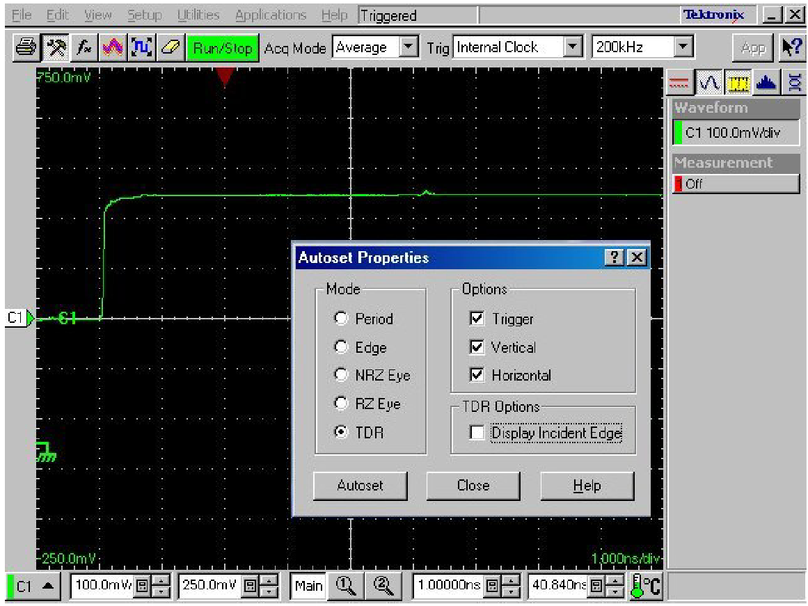
In order to verify that the mated cable impedance does not exceed the variance allowed in the standard, it is first necessary to establish the reference plane for the test. The standard specifies that this reference plane is the plug receptacle on the fixture being measured. Thus to establish the reference plane, we will look at a reflection from the reference open on the calibration fixture as follows:
- Connect C1 to the reference open of the USB 3 calibration fixture as shown in figure 3.2a.
- Do a single ended preset on C1 (by pressing the “C1” Preset button in the TDR Setup dialog) and set the TDR units to volts (V) - see figure 3.2b.
- Press the “TDR Autoset Properties” button in the TDR Setup dialog and then select an Autoset Mode of “TDR” and uncheck the “Display Incident Edge” box and press the Autoset Button in the Autoset Properties dialog.
- Set the horizontal scale to 1 nsec/div and align the reflected edge such that the start of its rising edge is at 1 div (= 1 nsec) as in figure 3.2c.
THE IMPEDANCE REFERENCE PLANE IS NOW AT 1 NSEC (DIVISION 1) ON THE OSCILLOSCOPE DISPLAY. DO NOT CHANGE THE HORIZONTAL POSITION OR SCALE.
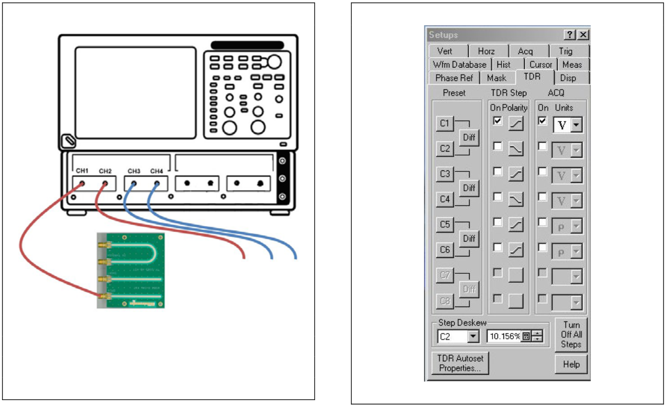
Figure 3.2b: TDR Setup for Impedance Reference Plane
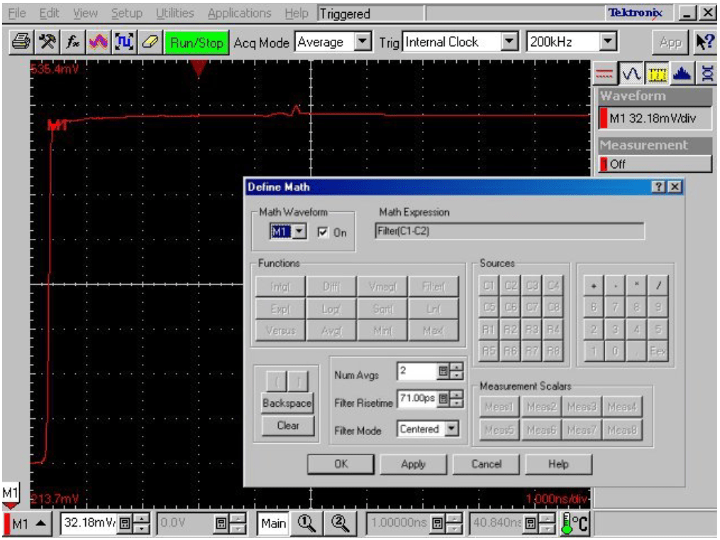
In order to get the best accuracy for the mated cable impedance waveforms we will use the Z-Line capabilities of IConnect®. This feature removes the effects of multiple reflections for TDR based impedance measurements. The Z-Line algorithm requires that you provide not only the reflected waveform of the Device Under Test (DUT) but also a reference step waveform. We will use an open at the end of the SMA cables as this reference.
- Disconnect all SMA cables from the test fixtures.
- Turn on a negative TDR step on C2 and turn off the display of all channels (in the TDR setup dialog).
- Set up a Math Waveform – M1 = FILTER(C1-C2) – that has a rise time filter of the value obtained in section 3.1.3 above and turn it on. (see figure 3.2d).
- Start IConnect and set it up to acquire data from the DSA8200.
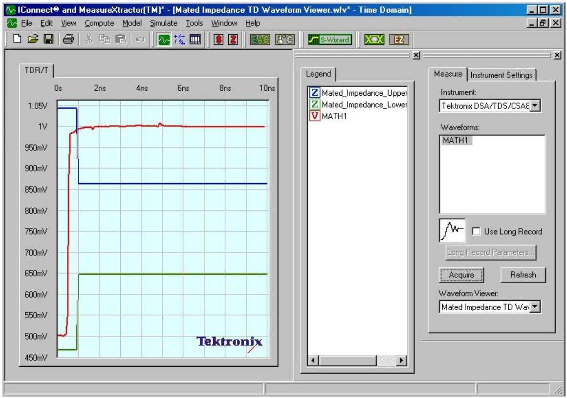
- Open the “Mated Impedance TD Waveform Viewer.wfv” file.
- Acquire Math1 (the Z-Line reference Step) in this viewer and rename this waveform “Step” (see figure 3.2e).
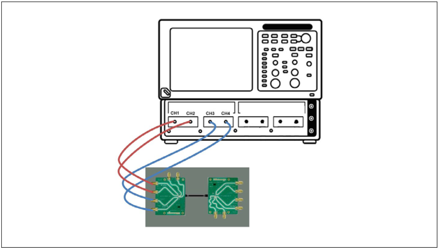
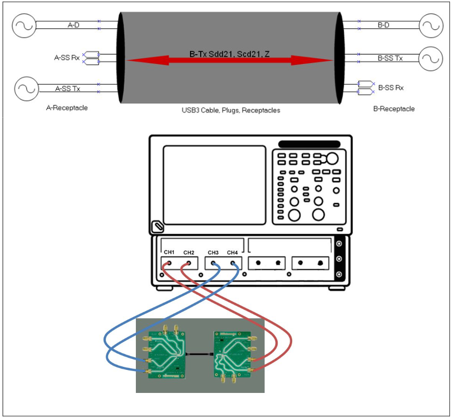
- Next, connect C1 and C2 to the Tx port of the A Receptacle Fixture and connect the cable to be tested between the A-Receptacle and the B-Receptacle. Make sure to install 50 ohm terminations to all unused connections on both fixtures (see figure 3.2f).
- Acquire Math1in this viewer and rename it A-Tx.
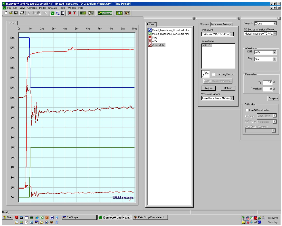
- Using the Z-Line Computation dialog, convert the A-Tx voltage waveform to impedance using the following settings:
- DUT waveform: A-Tx
- Step waveform: Step
- Z0 : 100 Ω
- Threshold: 35%
The resulting impedance waveform (ZLine_A-Tx) is shown in figure 3.2g - Repeat steps 11-13 for the A-Rx, B-Tx and B-Rx ports of the test setup.
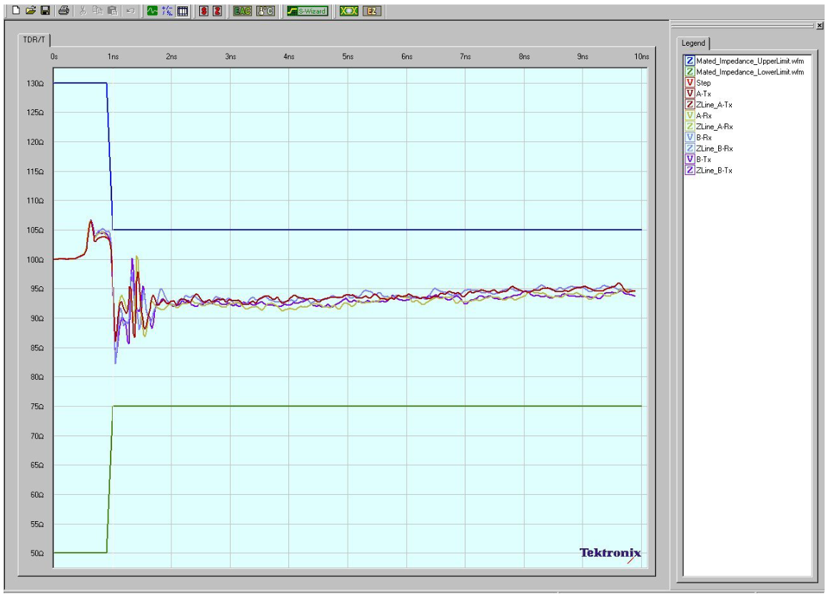
- Hide or delete the voltage waveforms and control dialogs. The resulting waveform viewer shows whether the mated impedance of all 4 ports of the super speed channels (A-Tx, A-Rx, B-Tx and B-Rx) are within the impedance limits specified by the standard. (see figure 3.2h).
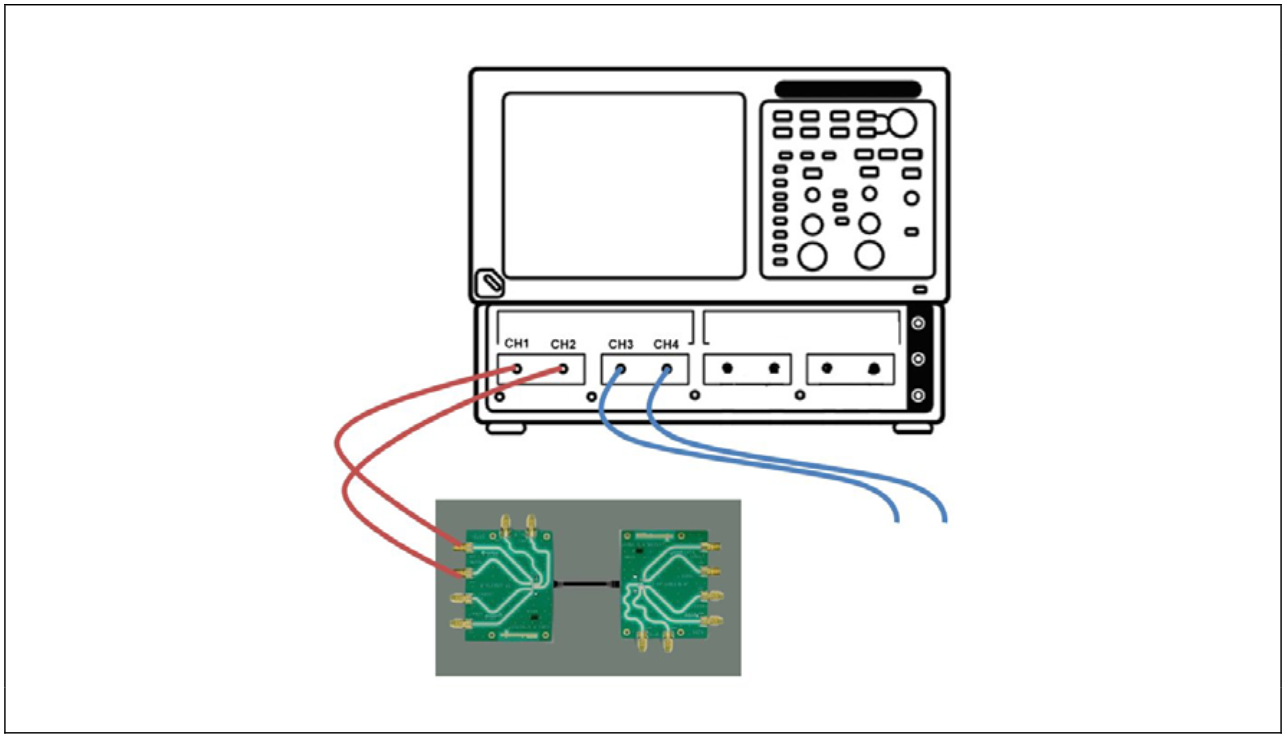
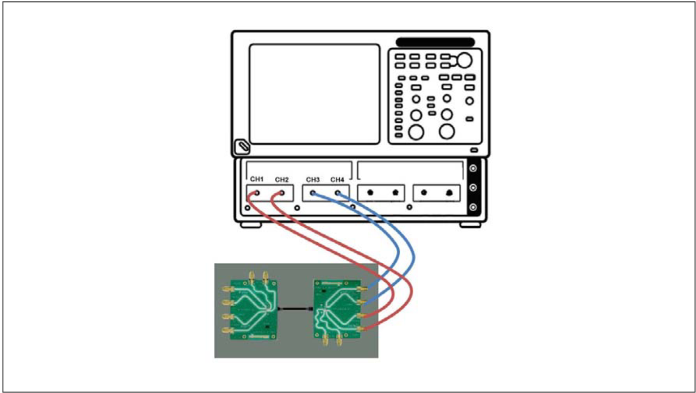
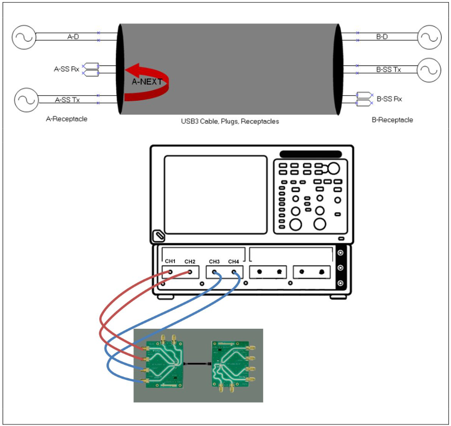
- Connect C1, C2 to the A-Tx port and C3, C4 to the A-Rx Port; the cable under test should be connected to the A- and B-receptacle fixtures and all unused connections on these fixtures should be terminated to 50. (See figure 3.3a)
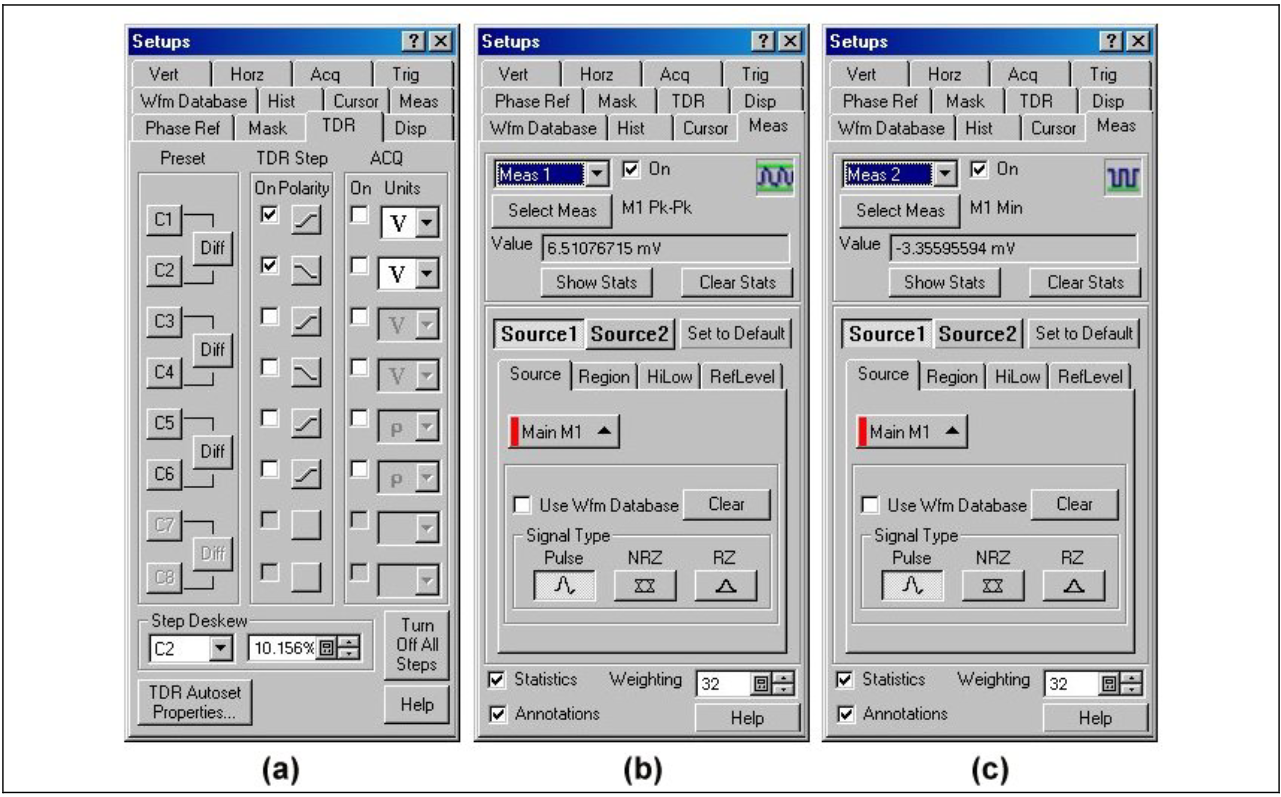
- In the TDR setup menu verify that C1 and C2 steps are enabled – C1 being a positive step and C2 a negative step. All four channels (C1 – C4) should be turned off and the units should be volts (V) – see figure 3.3b (a).
- Define Math Waveform 1 (M1) to be:
M1 = Filter(C3-C4)
where the rise time filter value is as determined in section 3.1.3. (It is not necessary to display this signal.) - Define two measurements to be used to normalize the crosstalk signal as follows – see figure 3.3b (b) and (c):
- Meas1 = pkpk(M1); pulse peak-to-peak
- Meas2 = min(M1); pulse minimum
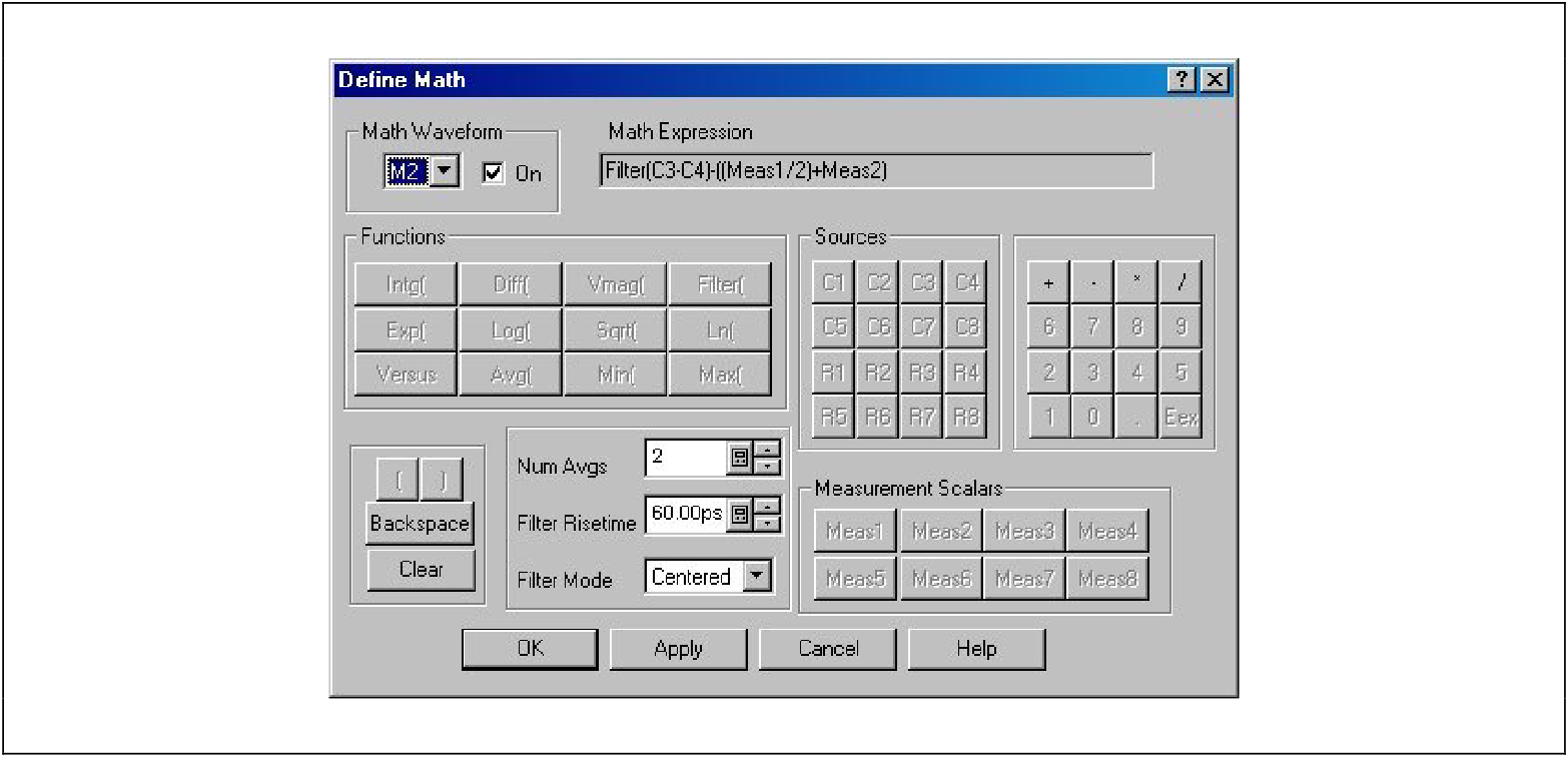
- Define Math Waveform 2 (M2) to be - see figure 3.3c:
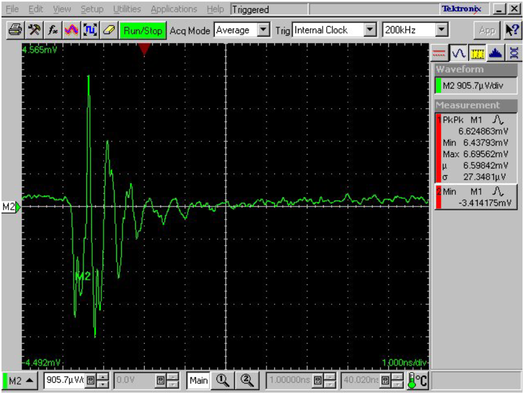
M2 = Filter(C3-C4)-((Meas1/2)+Meas2), where the rise time filter value is as determined in section 3.1.3.
Turn on the display of this signal. The normalized signal should appear similar to 3.3d. - Start IConnect and set it up to acquire data from the DSA8200.
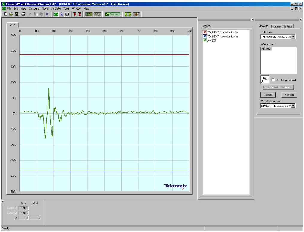
- Open the “DDNEXT TD Waveform Viewer.wfv” file. (Notice that the limits for time domain crosstalk are ± 3.75mv. Differential steps for all Tektronix TDR sampling modules are 500 mV. 1.5% of 500 mV = 7.5 mV.)
- Acquire Math2 (the normalized time domain A-NEXT waveform) in this waveform viewer and rename this waveform “A-NEXT” (see figure 3.3e).
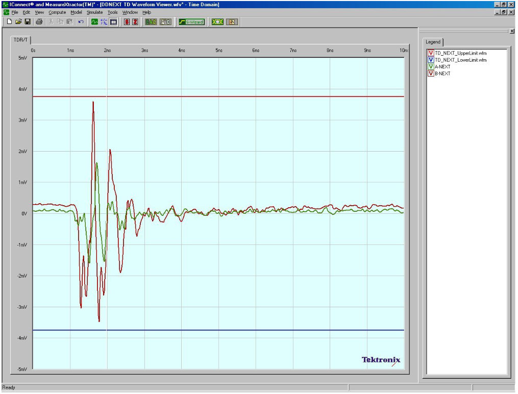
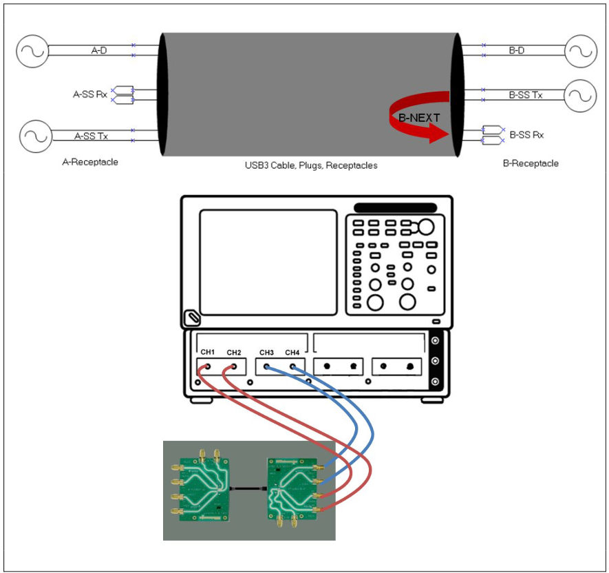
- Connect C1, C2 to the B-Tx port and C3, C4 to the B-Rx Port; the cable under test should be connected to the A- and B-receptacle fixtures and all unused connections on these fixtures should be terminated to 50. (See figure 3.3f)
- Acquire Math2 (the normalized time domain B-NEXT waveform) in the current waveform viewer and rename this waveform “B-NEXT”.
- Hide the unused control dialogs and if desired rescale the plot to +/- 5 mv and 0 to 10 ns. The resulting waveform viewer shows whether the super speed channel near end crosstalk is within the limits specified by the standard. (see figure 3.3g).
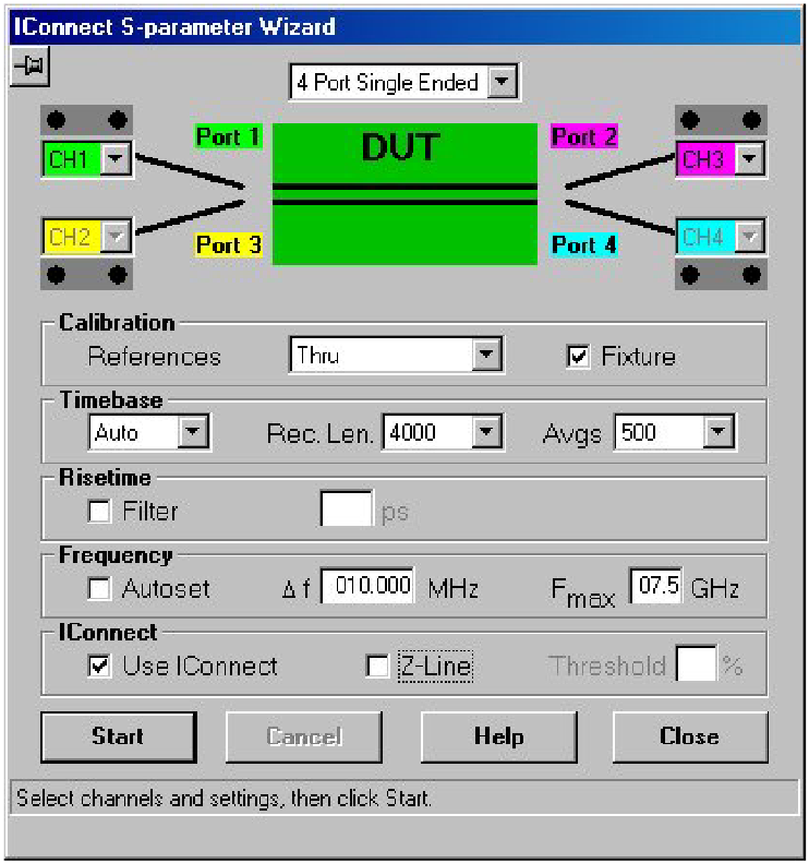
- Network Type: 4 Port Single Ended
- Calibration: Thru
- Timebase: Auto, Rec Length=4000, Avgs=500
- Risetime: (no filter)
- Frequency: (no Autoset), △f = 010 MHz, Fmax = 07.5 GHz
- IConnect: Use IConnect, (no ZLine)
- Start IConnect and open the “SS Channel Waveform Viewer.wfv” frequency domain waveform viewer file. This loads the Sdd21 and Scd21 limit waveforms. Turn on labels for the limit waveforms and position these labels adjacent to the waveforms. (Adding labels and changing the properties of a waveform can be done by right clicking on the desired waveform.) Since the limit tests are magnitude only; hide the phase pane of this display.
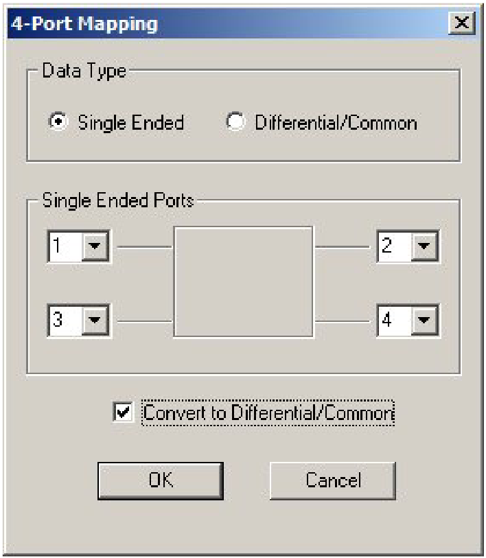
- Import the touchstone file associated with the A-Tx channel – “DUT_1_SE.s4p”. (Use the default port assignments and check the “Single Ended” and “Convert to Differential/Common” checkboxes as shown in figure 3.5.1a.
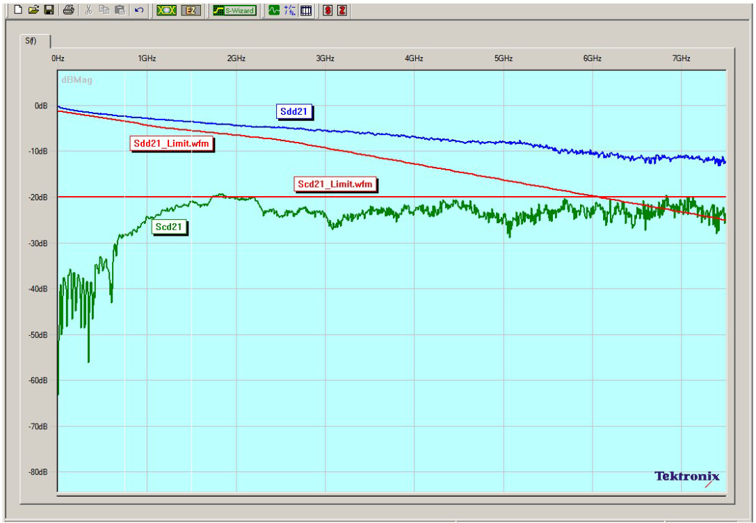
- We are only concerned with Sdd21 and Scd21, so delete the other 14 S-Parameter waveforms. Turn on labels for Sdd21 and Scd21 and position them next to the appropriate waveforms. If desired change the colors of Sdd21 and Scd21. You may also wish to turn off the cursor readout and waveform legend display. The resulting waveform viewer window should appear similar to figure 3.5.1b. (For this example, the cable passes the A-Tx insertion loss limit test, but (barely) fails the common mode conversion limit test.)
PRINT OR COPY THE FREQUENCY DOMAIN WAVEFORM VIEWER AS THE A-TX INSERTION LOSS AND COMMON MODE CONVERSION PORTION OF THE COMPLIANCE TEST REPORT. - Repeat steps 1-3 importing the touchstone file associated with the B-Tx channel – “DUT_2_SE.s4p” and save the B-TX INSERTION LOSS AND COMMON MODE CONVERSION limit test results.
- Start IConnect and open the “SS NEXT Waveform Viewer.wfv” frequency domain waveform viewer file. This loads the near-end crosstalk limit waveforms. Turn on labels for the limit waveforms and position these labels adjacent to the waveforms. (Adding labels and changing the properties of a waveform can be done by right clicking on the desired waveform.) Since the limit tests are magnitude only, hide the phase pane of this display.
- Import the touchstone file associated with the A-NEXT – “DUT_4_SE.s4p”. (Use the default port assignments and check the “Single Ended” and “Convert to Differential/Common” checkboxes as shown in figure 3.5.1a. We are only concerned with Sdd21, so delete the other 15 S-Parameter waveforms and rename the Sdd21 waveform to “A-NEXT”.
- Import the touchstone file associated with the B-NEXT – “DUT_3_SE.s4p”. We are only concerned with Sdd21, so delete the other 15 S-Parameter waveforms and rename the Sdd21 waveform to “B-NEXT”.
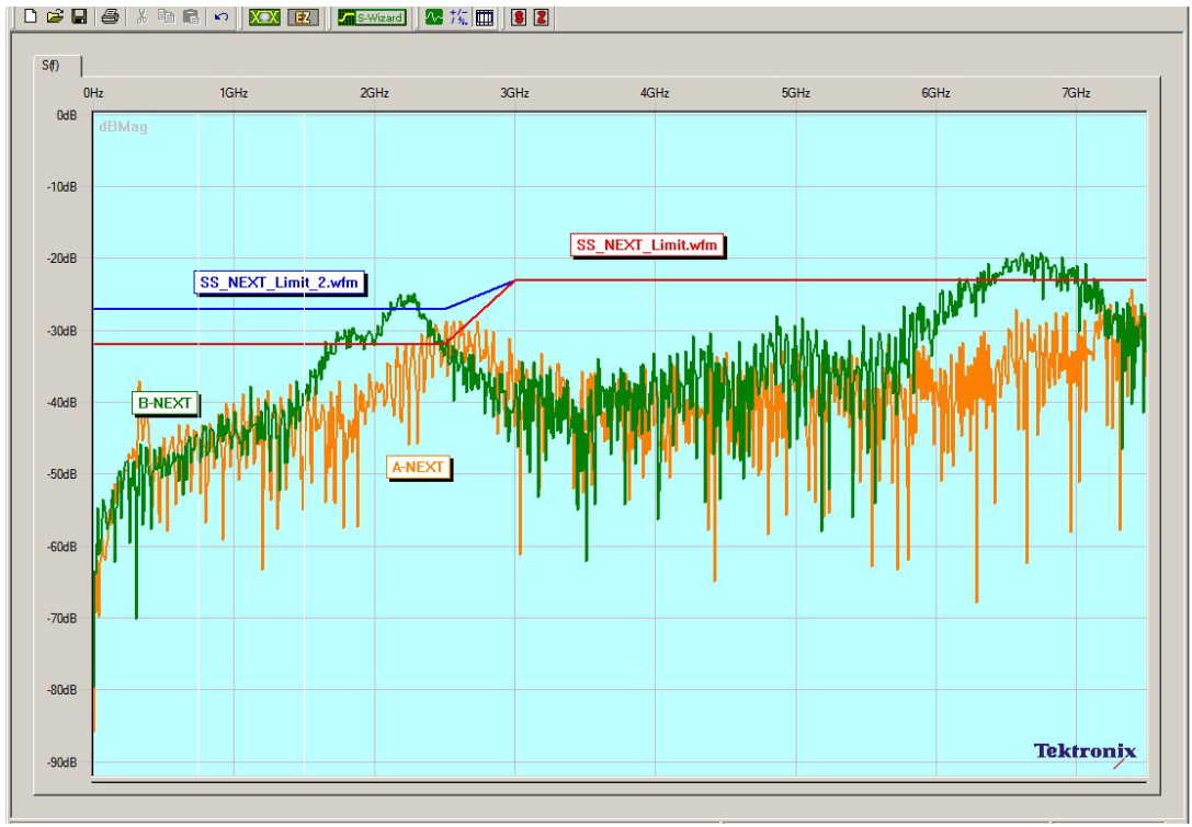
- Turn on labels for A-NEXT and B-NEXT and position them next to the appropriate waveforms. If desired change the colors of A-NEXT and B-NEXT. You may also wish to turn off the cursor readout and waveform legend display. The resulting waveform viewer window should appear similar to figure 3.5.2. (For this example, the cable provisionally passes the A-NEXT limit test – assuming that it passes the Time Domain NEXT limit test. The cable fails the BNEXT limit test.)
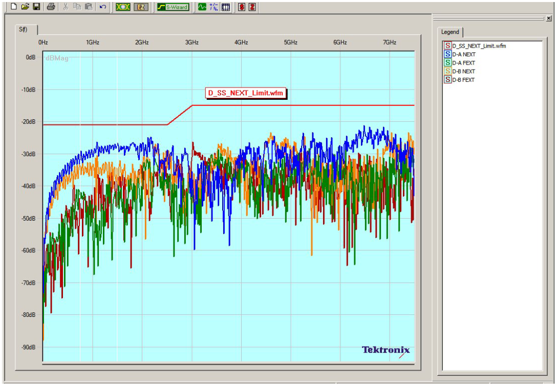
PRINT OR COPY THE FREQUENCY DOMAIN WAVEFORM VIEWER AS THE SUPER SPEED NEAR-END CROSSTALK PORTION OF THE COMPLIANCE TEST REPORT. - Start IConnect and open the “D-SS NEXT Waveform Viewer.wfv” frequency domain waveform viewer file. This loads the high-speed to super-speed crosstalk limit waveform. Turn on the label for the limit waveform and position it adjacent to the waveform. Since the limit tests are magnitude only, hide the phase pane of this display.
- Import the touchstone file associated with the D-A NEXT – “DUT_5_SE.s4p”. (Use the default port assignments and check the “Single Ended” and “Convert to Differential/Common” checkboxes as shown in figure 3.5.1a. We are only concerned with Sdd21, so delete the other 15 S-Parameter waveforms and rename the Sdd21 waveform to “D-A NEXT”.
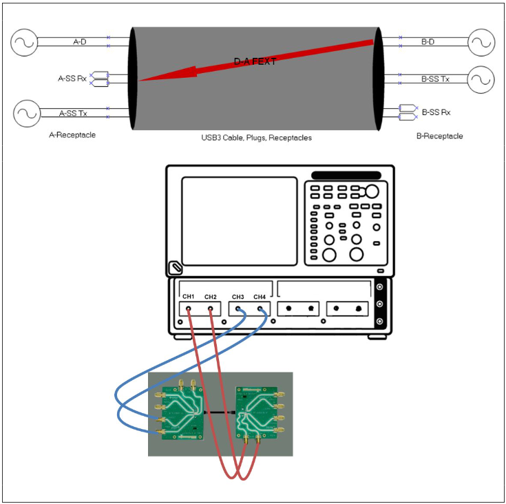
- Import the touchstone file associated with the D-A FEXT – “DUT_6_SE.s4p”. We are only concerned with Sdd21, so delete the other 15 S-Parameter waveforms and rename the Sdd21 waveform to “D-A FEXT”.
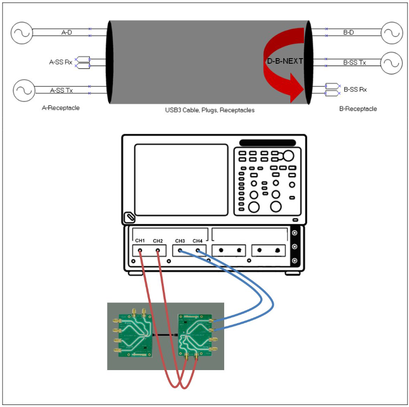
- Import the touchstone file associated with the D-B NEXT – “DUT_7_SE.s4p”. We are only concerned with Sdd21, so delete the other 15 S-Parameter waveforms and rename the Sdd21 waveform to “D-B NEXT”.
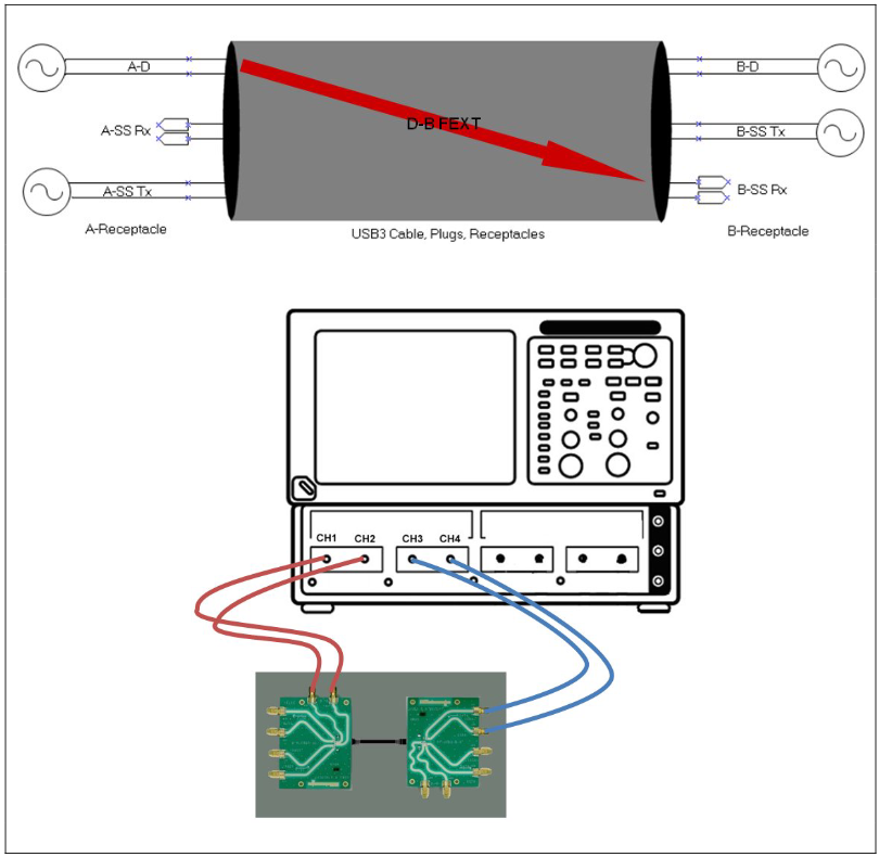
- Import the touchstone file associated with the D-B FEXT – “DUT_8_SE.s4p”. We are only concerned with Sdd21, so delete the other 15 S-Parameter waveforms and rename the Sdd21 waveform to “D-B FEXT”.
- If desired change the colors of the near- and far-end crosstalk waveforms. You may also wish to turn off the cursor readout. The resulting waveform viewer window should appear similar to figure 3.5.3. (For this example, the cable passes all high-speed to super-speed crosstalk limit tests.)
PRINT OR COPY THE TIME DOMAIN WAVEFORM VIEWER AS THE MATED IMPEDANCE PORTION OF THE COMPLIANCE TEST REPORT.
3.3 Differential Near End Crosstalk (DDNEXT) for Super Speed Channels Time Domain Tests
This test is only required only if the frequency domain DDNEXT test violates the lower limit, but passes the upper limit test, but since the instrument is setup with the appropriate step and acquisition alignment, rise time filtering and reference plane, we will do this test just in case.
As with the mated cable differential impedance tests, the DDNEXT time domain measurements are specified for a 50 psec rise time step. This signal is applied to the transmit channel on the A- and B-receptacles and the resulting crosstalk measured on the corresponding receive channel.
The time domain crosstalk limit is defined to be < 1.5% of the applied step amplitude. Since the crosstalk may be asymmetric, for limit testing it is easiest to normalize the acquired crosstalk signal to center it about 0 volts. This is accomplished by applying the following formula:

We will now use IConnect to compare the normalized time domain crosstalk to the limits specified by the USB 3 standard.
PRINT OR COPY THE TIME DOMAIN WAVEFORM VIEWER AS THE TIME DOMAIN NEAR END CROSSTALK PORTION OF THE COMPLIANCE TEST REPORT.
3.4 Acquire S-Parameter Data Using IConnect SParameter Wizard
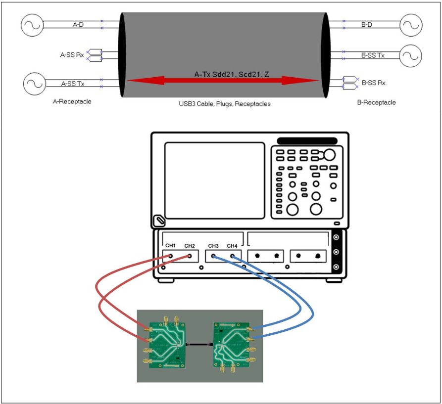
All of the frequency domain USB 3.0 cable compliance tests in this MOI utilize the IConnect S-Parameter Wizard to acquire the data necessary to generate the required differential S-Parameter data. This general purpose tool allows the user to acquire time domain data for 1-, 2-, or 4-port single-ended or 1-, or 2-port differential networks and then convert these into S-Parameter files and generate Touchstone files.
For the purposes of this MOI, the USB3 cable is treated as eight 4-port single-ended subnetworks. (Doing single ended measurements and then converting the network to differential simplifies the automated deskew that must be done.) Approved test fixtures are designed to have well matched traces for all signals in the network. This implies that one can do a single system deskew and calibration for all sub-networks. The S-Parameter Wizard thus does this deskew and calibration for the first sub-network and uses this for all eight sub-networks.
With a complete set of single-ended 4 port s-parameter waveforms, it is a simple matter for IConnect to convert these to differential and mixed mode S-parameter waveforms for limit testing for conformance to the USB 3.0 standard.
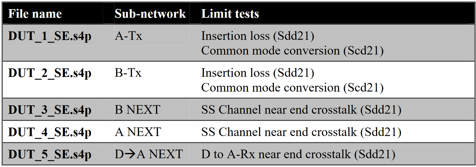
Shown below are the sub-network definitions as well as the system configurations for each sub-network. (The acquisition order for these sub-networks was chosen to minimize the amount of cable connection swapping that must be done.)
DUT1: A-Tx – used to measure Sdd21 and Scd21 for the A-Tx channel.
DUT2: B-Tx – used to measure Sdd21 and Scd21 for the B-Tx channel.
DUT3: B-NEXT – used to measure near end crosstalk for the B receptacle.
DUT4: A-NEXT – used to measure near end crosstalk for the A receptacle.
DUT5: D-A NEXT – used to measure near end crosstalk between the high-speed and the A-Rx super speed channel.
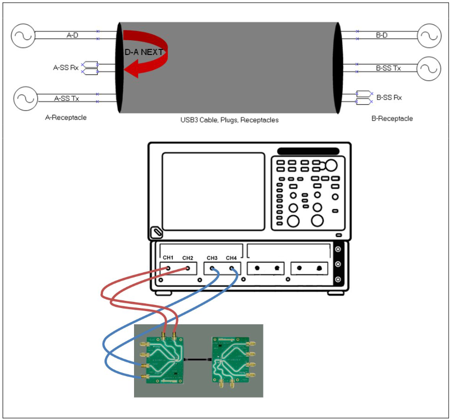
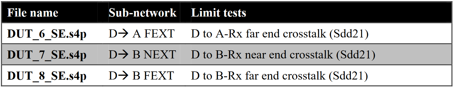
DUT6: D-A FEXT – used to measure far end crosstalk between the high-speed and the A-Rx super speed channel.
DUT7: D-B NEXT – used to measure near end crosstalk between the high-speed and the B-Rx super speed channel.
DUT8: D-B FEXT – used to measure near end crosstalk between the high-speed and the B-Rx super speed channel.
To acquire the S-Parameter data for these sub-networks, start the IConnect S-Parameter Wizard and set it up with the following parameters (as shown in figure 3.4.1):
Acquire the 8 sub-networks required by connecting the system as shown in the diagrams above as eight DUTs (devices under test). At the conclusion of “DUT8” exit the SParameter Wizard by clicking on the “Cancel Button” when asked to connect DUT9.
The S-Parameter Wizard will generate a plethora of time domain and frequency domain files. The results files that are required for limit testing of the frequency domain measurements are the following 8 Touchstone files:
3.5 Frequency Domain Limit Tests
Having acquired all of the sub-network waveforms necessary for the USB 3 frequency domain limit tests, all that remains is to convert these networks to the 90Ω characteristic differential impedance (Z0) of USB 3 (vs. the TDR systems native 100Ω differential impedance) and then compare the appropriate S-Parameter waveforms.
(NOTE: impedance renormalization is a function that will be in a soon to be released version of the IConnect products.)
3.5.1 Super Speed Channel Insertion Loss and Common Mode Conversion
To complete the insertion loss (Sdd21) and common mode conversion (Scd21) limit tests for the super speed channels:
3.5.2 Super Speed Channels Near-End Crosstalk
To complete the Super Speed Near-End Crosstalk limit tests for the super speed channels:
3.5.3 High Speed to Super Speed Channel Near-End and Far-End Crosstalk
To complete the High Speed to Super Speed Channel Near-End and Far-End Crosstalk limit tests:
PRINT OR COPY THE FREQUENCY DOMAIN WAVEFORM VIEWER AS THE HIGH SPEED TO SUPER SPEED NEAR- AND FAR-END CROSSTALK PORTION OF THE COMPLIANCE TEST REPORT.
1 At the current release of this document, the “Universal Serial Bus 3.0 Connectors and Cable Assemblies Compliance Document” is awaiting final approval by the USB-IF Compliance Committee. When this document is approved, we will update the MOI to reflect any changes as necessary.
2 Since the Differential Far-End Crosstalk between SS pairs is informative, this test is not documented in this MOI.
3 The procedures in this MOI can be used with any 8000 series sampling oscilloscope that is running Windows XP and at least version 5.0.0 of the scope firmware.
4 Tektronix part number 015-0560-00 or similar
5 The testing can be performed with two 80E04s, with 2 ps matched cables. However this will impact accuracy and dynamic range.
6 2 ps matched cables are required