Designers who work with serial buses and systems know that critical specifications, especially data rates, are constantly advancing. Higher speeds mean shrinking operating margins. These in turn contribute to diminishing tolerances that complicate the pursuit of flawless interoperability among system elements. Measurements – in the lab, during compliance testing, and in production – play a major role in promoting interoperability. Testing has become the focus of industry- wide attention as designers strive to develop technologies and measurement procedures that maximize both performance and interoperability
Losses, Aberrations Pursue Serial Signals
The common serial data receiver, an element used by the hundreds in digital systems of all kinds, poses one of the biggest challenges for designers who need to exercise and characterize emerging devices. As usual, the fundamental questions are "Will the receiver work in real world conditions?" and "What is its worst-case behavior?" In actuality, the typical serial data receiver often operates in a real world that essentially is the worst case.
Why? Because signals traversing a given transmission link tend to degrade in proportion to their clock rate and the length of the transmission path. Even the most carefully controlled link has more impact on, for example, a 6.0 Gb/s signal than a 500 Mb/s signal. Next-generation serial standards will see data rates escalate to 6.0 Gb/s and beyond, with no end in sight. Serial data signals are demanding more and more of the circuit elements that deliver them.
Equally important, real-world applications often stray from the ideal of a controlled-impedance signal path with minimal length and minimal disruptions. Practical manufacturing economies dictate the use of relatively lossy media such as FR4 epoxy circuit boards. Packaging requirements rather than electrical considerations drive circuit layouts. And mass-produced cables and connectors routinely trade off signal fidelity in favor of cost-effective simplicity. System designers knowingly balance transmission path integrity against the realities of cost and competition.
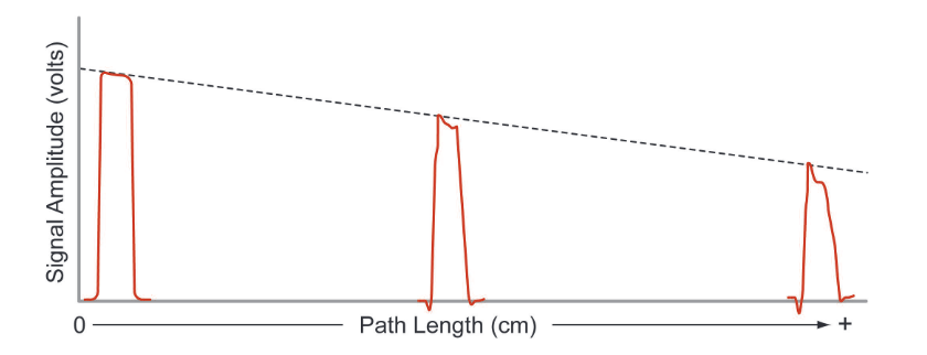
Consider just one effect of these choices, the impact of a lossy medium on the signals that pass through it. Figure 1 is a simplified image that illustrates conceptually what happens to a pulse as it travels the length of a transmission path. At high data rates the pulse amplitude decreases steadily over the length of the path, potentially reaching a level too low to guarantee accurate threshold decisions at the receiving end. In addition, effects such as edge degradation and overshoot (also shown) play a role in compromising the signal’s intelligibility at the receiving input.
What is the cause of these losses? A high-frequency signal that propagates through a long PCB trace experiences dramatic degradation due to the loss tangent of the circuit board’s dielectric material. A high loss tangent relates to high dielectric absorption, which increases attenuation at high frequencies. While Figure 1 does not denote the performance of a specific medium, its underlying message is that signals will suffer in proportion to the lossy characteristics of the medium.
Losses, inter-symbol interference, crosstalk, noise, jitter, it all adds up to a very threatening environment for a high-speed data signal. Figure 2 is a dual view showing the same serial data signal before and after transmission. The yellow trace is an eye diagram of the transmitter output. The eye is open and robust, with full amplitude and plenty of clearance around the decision points at the center of the view.
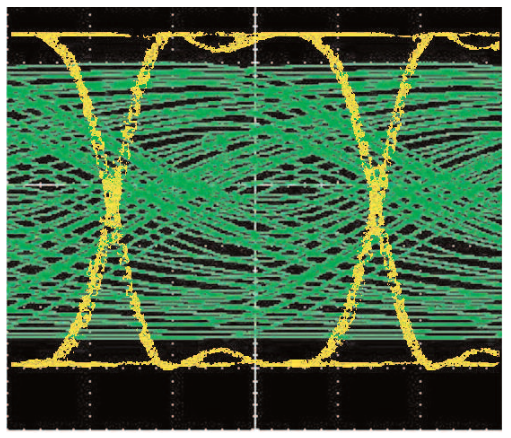
The transmitter trace is superimposed on the green trace, which though indistinguishable is also an eye diagram. This is the receiver input! All remnants of the eye opening have vanished. Yet somehow the receiver’s internal serializer/deserializer (SERDES) circuit needs to extricate usable binary data packets and clocks from this signal.
Obviously a signal such as the green trace in Figure 2 is unacceptable. Designers throughout the computing and communications industries have spent countless man-years looking for solutions to this problem. But ultimately these behaviors are a result of the physics of materials, electricity, and radiation. Until "perfect" drivers, cables, and transmission media are invented, designers must concentrate on either minimizing or counteracting the losses, or preferably both.
Three Strategies, Two Solutions
Three strategies have emerged to deal with the serial signal transmission challenges just summarized1:
- Signal conditioning to counteract attenuation and related losses
An approach known as de-emphasis2 (or alternatively, pre-emphasis) deals with signal degradation by recognizing its characteristics and applying counteracting amplitude changes in advance. Filtering (equalization) is another tool used to pre-empt anticipated signal losses due to the frequency response of the transmission medium
- Thorough stress validation of new designs, using externally-imposed "worst-case" signal conditions
As a new receiver design emerges, it is tested with signals containing jitter, noise, amplitude variations, and other stress-inducing characteristics. By monitoring a device's response, chiefly in terms of bit error rates, it is possible to pinpoint vulnerabilities that could appear in end-user applications.
- Rigorous compliance and interoperability testing
In the final analysis, interoperability under specified operating conditions is the most important attribute of all. Industry standards and compliance guidelines are the path toward this ideal. Serial product developers are urgently looking for solutions that will speed and simplify their compliance measurements while delivering accurate, repeatable results.
Each of these strategies depends on accurate measurements as part of either the design or evaluation process. Signal sources must provide known, controlled stimulus signals. Measurement tools, usually oscilloscopes and error rate testers, must monitor input and/or output ports and capture every signal detail.
A critical requirement in all of these strategies is a signal source that can drive the receiver with complex data patterns modified by de-emphasis and filtering as well as noise, jitter, and other imperfections. Two types of signal sources (sometimes supplemented by secondary sources for modulation and/or noise injection) span the receiver’s stimulus requirements:
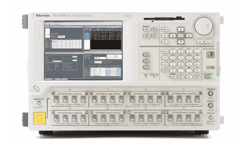
The Data Timing Generator (DTG, Figure 3), sometimes known as a pattern generator or logic source, delivers purely digital (binary) signals. Within the instrument, patterns may be created algorithmically or read from internal memory locations at test time. Signal amplitudes can be varied and rise and fall times are adjustable. In general, modulation, jitter, and noise must be supplied by an external device, though some instruments have built-in features to add controlled amounts of jitter to the signal. One key DTG advantage is its wealth of outputs – up to 32 channels on a single platform, which in turn can be synchronized using a master-slave configuration to yield up to 96 channels.
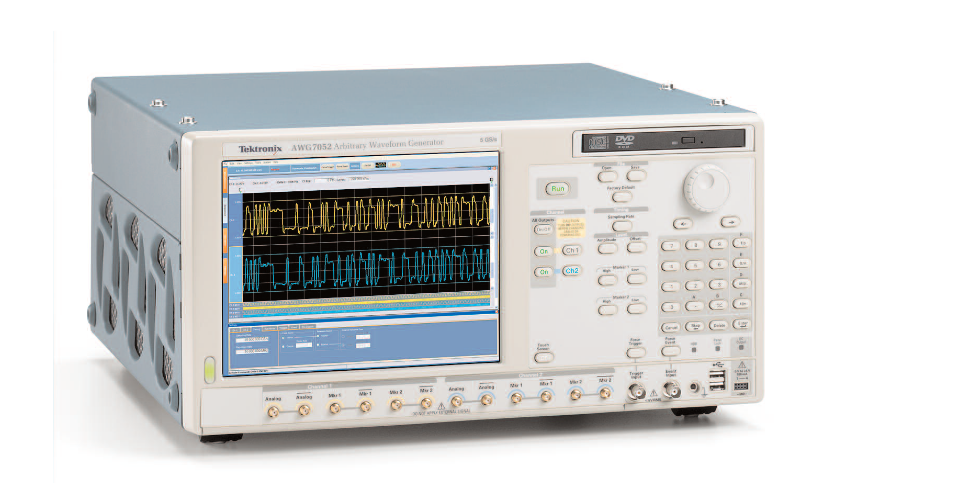
The Arbitrary Waveform Generator (AWG, Figure 4), a tool designed to output “analog” signals, is equally capable of sourcing digital patterns. However, the main data stream is generated by reconstructing sampled waveforms stored within the instrument’s memory. Assuming the instrument has sufficient bandwidth and sample rate, this technique allows aberrations and signal condition to be embedded into the signal, eliminating the need for external sources. AWGs commonly include several digital marker outputs that can act as additional data sources. The balance of this document will examine some techniques that use these tools to help designers implement effective test strategies.
Inter-Symbol Interference (ISI) Meets Its Match In De-Emphasis
Inter-symbol interference (ISI) can occur when a group of successive serial bits of the same state cause a buildup of energy in transmission components, with the result that pulses begin to spread in time and even overlap. Eventually the receiver has difficulty distinguishing changes of state. ISI began to plague serial bus transmission channels as bit rates accelerated into the gigabit range. Detecting and eliminating ISI has been the focus of a tremendous amount of research effort.
The accepted cure for ISI is de-emphasis. The de-emphasis technique assumes that, for any series of bits having the same binary state, the first bit (known as the transition bit) must have a greater amplitude than the bits that follow it to compensate for the frequency characteristics of the transmission line and improve signal fidelity at the receiver input. By making the transition bit higher in amplitude than the subsequent bits, the signal will arrive at the receiver pins with an "open eye."
Like any other treatment that affects signal amplitude and wave shape, an emerging serial device’s response to de-emphasis must be evaluated thoroughly during the design phase. Moreover, de-emphasis measurements are part of most compliance test regimes, including those for PCI Express II, Ethernet, XAUI and more.
The DTG has long been a solution of choice for de-emphasis evaluation. Although the DTG requires two differential channels to deliver one signal with deemphasis, and a total of eight channels for four lanes, a modern multi-output DTG can be equipped with more than enough outputs to do the job.
A typical DTG configuration might have 16 channels – sufficient for four “lanes” of a serial bus such as PCI Express. With the growing importance of multi-lane serial architectures (the PCI Express standard encompasses variants having up to 16 lanes) as a solution for maximizing data throughput, the DTG’s future in de-emphasis testing is assured.
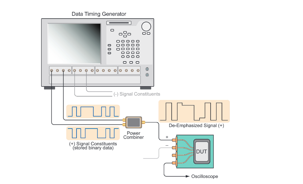
De-emphasis testing with a DTG requires an external power combiner to mix two synchronized data streams and produce a single composite output. The test setup is shown in Figure 5 (note that only the “plus” side of the differential pair is shown in its entirety; the “minus” side mirrors this arrangement). It is important to reiterate here that the constituent data is stored within the DTG as individual binary bits that are read in each operational cycle, such that a "1" in the DTG memory becomes a single "1" in the pattern.
Another Way to Produce De-Emphasis Signals
An alternative method of producing the de-emphasis signal (and many other effects) is emerging thanks to the arrival of high-speed AWGs delivering sample rates up to 24 GS/s. These instruments are capable of delivering data rates consistent with the needs of serial standards in the second generation and beyond. The AWG method of producing the de-emphasis signal is entirely different from that of the DTG, although the resulting signal applied to the DUT is identical.
Full-featured modern AWGs are known as directsynthesis platforms. They generate a signal by reading a sequence of samples, each defining one analog voltage value, from a random-access memory. A succession of these samples reconstructs a waveform. This may be a sine wave, a ramp or triangle… or a serial data stream. The waveform samples are typically created with the help of a software editing tool or they may be imported from an oscilloscope that has acquired them from reference measurements. Most importantly, the stored signal data can be modified to introduce de-emphasis or other characteristics.
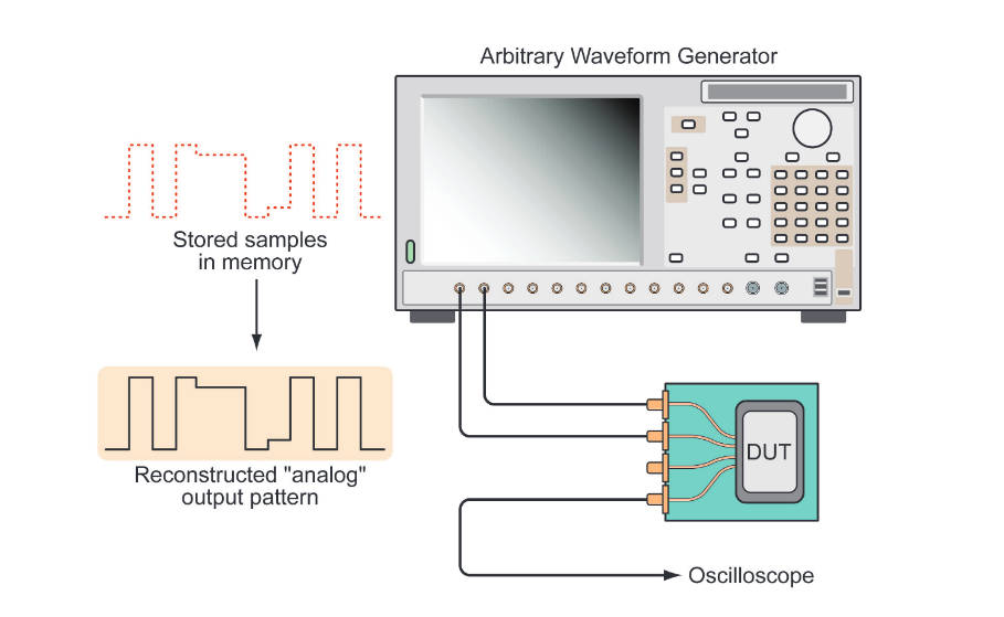
Because the stored signal can incorporate the deemphasis, there is no need to generate and externally combine two constituent data streams for each side of the differential signal. Two complementary AWG analog outputs are used to drive the differential inputs of the DUT. As Figure 6 shows, this is a simpler arrangement than that of the DTG-based configuration.
Digital marker outputs accompany the analog outputs on most high-speed AWGs, enabling the instruments to serve as the stimulus source for testing on multi-lane serial devices. These markers offer excellent timing precision as well as variable output levels. In use they perform very similarly to the digital outputs of the Data Generator.
Stress Testing Calls For Re-Shaping Signals
Stress testing provides necessary proof that a newlydesigned serial element can withstand the rigors of high-speed transmission and still deliver acceptable bit error rates. Even the best signal path can allow some noise to intrude or admit just enough crosstalk to cause jitter. The receiver must be able to reject these effects as much as possible. Signal sources play a big role in stress testing, since they provide signals intentionally laden with noise and distortion. These emulate effects ranging from jitter to overshoot.
Jitter is a phenomenon that can have drastic effects on circuit behavior, since it tends to “smear” edge placements and narrow the eye opening. The importance of jitter measurement is such that jitter features and tools are now integrated into many signal sources including DTGs and AWGs. A DTG-based setup can deliver a fixed jitter profile that meets the needs of many applications. However, if jitter modulation is required, an external waveform generator must provide the modulating signal.
By using the direct synthesis (AWG) technique to create signals that represent what data looks like after propagation, transmission line, and system effects have taken their toll, it is possible to eliminate the ancillary equipment formerly required for modifying and modulating DTGproduced signals. With a suitable direct-synthesis AWG, jitter in any form can be merged into the test signal itself. The effects of both random and deterministic jitter can be modeled. The AWG’s ability to vary imposed effects such as jitter in both quantitative and qualitative terms is also valuable, and easy to accomplish.
The same is true of noise and aberrations such as overshoot. Because the fundamental architecture of the AWG platform allows essentially any signal shape to be defined, the small details of signal behavior are easy to model. And though small, these details are exactly what make up a “real world“ signal. Using an AWG, it is possible to closely approximate the content of a signal that has passed through FR4 traces, connectors, and cables.
Compliance Testing
The direct-synthesis method lends itself to other important serial validation and compliance testing requirements. At this writing, AWG techniques have not yet been codified into industry standards dictating signal production for most serial compliance testing. Tests for de-emphasis, noise, and other effects rely on DTG-based methods. However, with the emergence of fast new platforms, new procedures are being researched and evaluated.
One class of compliance tests, though, has been shown to benefit from the use of analog signal sources.
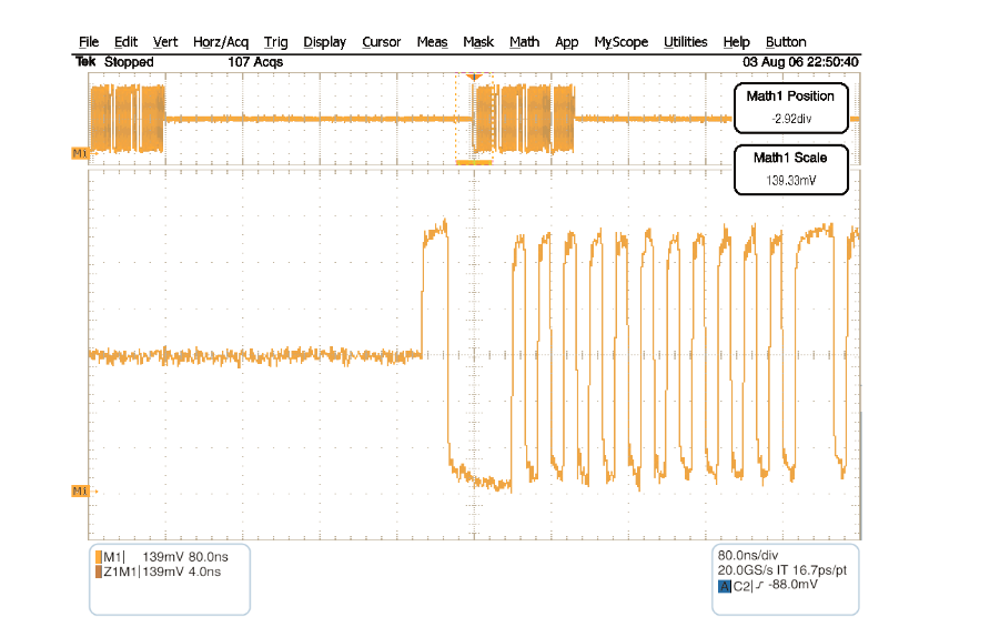
Multi-level signals with at least three states – high, low and idle – are common in out-of-band operations such as Serial ATA COMWAKE. This is an inter-device communication signal with bursts of data separated by an idle bus condition. The signaling occurs at lower frequencies than those encountered in the data path. The idle condition is essentially a tri-state level that falls between the true binary “1” and “0” values.
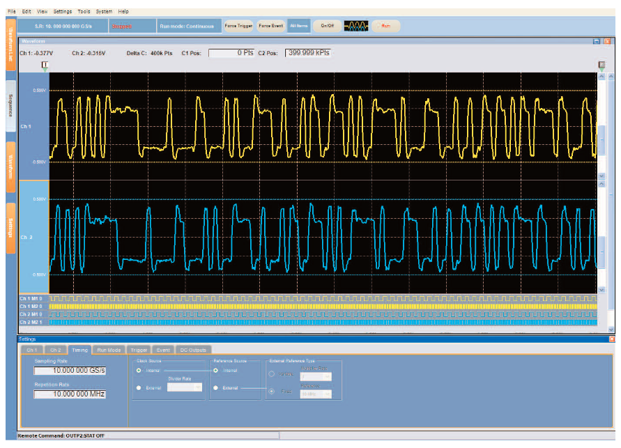
The idle state is exactly the sort of signal characteristic that brings out the strengths of an AWG. Given what we have already demonstrated with de-emphasis, it should be clear that the AWG can produce any needed voltage level on a sample-by sample basis. By eliminating the need for external signal modifiers such as power combiners, the AWG can generate an accurate tri-state voltage value just as easily as the binary pattern values that surround it. Figure 7 is an oscilloscope screen view showing an OOB signal generated by an AWG.
Conclusion
Testing receiver elements for the latest high-speed serial bus protocols, including SATA, PCI-Express and many more, is a challenge for engineers and their equipment alike. Specific tests are required before a product can receive “logo” certification under these standards. Established tools such as data or pattern generators have a proven track record for evaluation and compliance testing of these demanding technologies. Using external modifiers such as power combiners and noise generators, data generators can provide most of the necessary signal formats. Currently, most serial standards are based on results achieved with these purely digital tools. With fast digital-to-analog converters and faster sample clock capabilities, a new generation of arbitrary waveform generators is coming forward as a supplement to digital instrumentation – or even as an alternative. Since the testing requirement is, in effect, to replicate real-world transmission path effects, the AWG presents a compelling solution for the test problem. It can embed aberrations such as jitter and overshoot in the signal itself. And it can apply signal conditioning such as de-emphasis in the same way – as part of the original signal.
Research is underway to validate new approaches for design and compliance measurements using AWG sources.