Introduction
Clock recovery plays a significant role in making accurate test measurements, whether incorporated into the test setup or as part of the device under test. As most gigabit communication systems are synchronous, the data within them are timed against a common clock. Whether traveling across inches of circuit board or traversing continents on optical fiber, the relationship between the data and the clock they were timed against can become disturbed. By extracting clock directly from the data, signal regeneration at the receiver can be achieved correctly.
It is important to note that receivers typically improve the incoming data signal before passing it on. A decision circuit in the receiver retimes the data and squares up the pulses. This process depends on a clock signal that is synchronous with the incoming data. Clock recovery within the receiver achieves this goal, provided the retiming clock moves in the same way and at the same time.
PLL-based Clock Recovery
Different architectures exist for achieving clock recovery. The most common methodology used in measurement equipment is based on a phase-locked loop (PLL).The recovery circuit is used to derive a clock that is synchronous with the incoming data, dependent upon seeing transitions in the data. For data segments with runs of identical bits, the PLL must remain locked. The loop gain has the most significant effect on the loop bandwidth; any filtering within the loop filter typically has a secondary effect. It should be noted that the transition density of the incoming data affects the amount of energy entering the loop and, therefore, the loop characteristics. The consequence is that loop bandwidths in compliance testing can change depending on the transition density of the pattern chosen.
The system transfer function performs a low-pass filtering operation on the phase modulation of the input signal, while the error-response transfer function performs a high-pass filtering function. The loop tracks input phase modulation within the loop bandwidth while failing to track phase modulation outside the bandwidth. This enables the loop to track low-frequency jitter and ignore high-frequency jitter outside the loop bandwidth of the PLL.
One measure of the jitter tracking characteristic of a PLL is the loop bandwidth (LBW), often measured as the point where the transfer of 'jitter in/jitter out' is -3 dB. However, this is not the only way that loops are defined.
A wide LBW improves jitter tolerance, while a narrow LBW removes more jitter from the recovered clock, which is beneficial to downstream synchronizers but impairs jitter tolerance. Although a wide LBW seems ideal, it is usually cost and technology dependent. Wide LBWs also contribute more noise or random jitter. Current LBWs used in measurements are typically in the range of 1 to 10 MHz.
The Ups and Downs of Clock Recovery
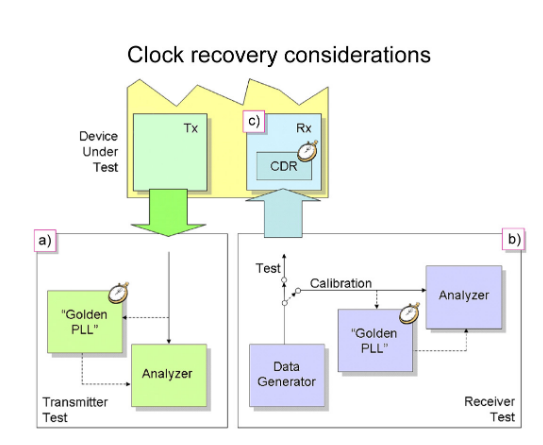
It is important to note how clock recovery is used in measurements and what could go wrong. On the transmitter testing side, for example, clock recovery is often required for two primary reasons either because no clock signal is available to act as a test equipment trigger, or because standards require jitter measurements to be made with a specific LBW (see Figure 1, part a). The intention of the latter is that a system receiver, like a BERTScope BSA Series, will contain clock recovery that tracks out some of the incoming jitter, so transmitter test-ing should only be concerned with high-frequency jitter that a receiver would not track. See Figure 1.
Thus, for signals under test with jitter components near the LBW of the clock recovery, an incorrectly set LBW can result in inaccurate jitter measurements. Sometimes standards imply use of clock recovery in testing by either referring to a 'golden PLL' or by specifying measurement of jitter 'after application of a single-pole, high-pass, frequency weighting function that progressively attenuates jitter at 20 dB/decade below a frequency of ((bit rate)/1,667)'.
Spread-spectrum clocking (SSC) spreads the energy of the clock (and the data) over 0.5% of the fre-quency band, lowering the average power at a given frequency in the spectrum. This helps products to comply with regulatory requirements for radiated and conducted emissions. For a receiver to successfully track out SSC, it must be able to track the modulation, including its harmonics, to avoid eye closure. If the loop response fails to sufficiently track SSC or there is an incorrect delay between the clock and data path, the test eye will be smeared closed.
Incorrect peaking (the region near the LBW where the jitter output of a clock recovery device can be greater than the jitter input) may amplify the amount of jitter measured. Additionally, trigger delay in the test equipment relative to the incoming data signal can cause incorrect amounts of jitter to be measured. For example, a fixed delay in the measurement system could cause additional apparent jitter to be measured. The additional jitter magnitude depends on the jitter frequency relative to the amount of delay.
At the receiver end, clock recovery can appear in either the device under test or as part of the test equip-ment calibration procedure. In the device under test, clock recovery is frequently present, and usually exercised in testing (see Figure 1, part b) using stress and sinusoidal jitter. In the case of sinusoidal jitter, testing is typically to a template whereby more jitter is applied at lower modulation frequencies and/or less jitter at higher frequencies
Problems would include an incorrectly designed LBW in the receiver that could cause a jitter tolerance template to fail. Incorrect slope to the tracking response may not follow SSC accurately enough, resulting in a test eye that is smeared shut and causing bit errors to occur.
Clock recovery is frequently used in the test equipment setup and calibration of a receiver's jitter toler-ance, or stressed eye, signal (see Figure 1, part c). Sinusoidal jitter is usually set to a frequency above the LBW of the clock recovery during calibration. However, an incorrect LBW may cause the wrong amount of stress to be set, resulting in either under- or overstressing the device being tested and increasing the likelihood of customer rejection or yield issues, respectively
From all these situations, it is easy to conclude that the LBW setting is critical and can have a significant impact on the observed jitter in measurement. Varying the loop bandwidth can give an indication of the jitter spectrum. Testing with very narrow LBWs can show all the jitter a transmitter under test is creating. Testing with very wide LBWs, on the other hand, indicates only the jitter that a transmitter produces that its intended system receiver is not able to filter out with its own PLL. Typically, the latter clock recovery is specified in compliance testing. A system designer is mainly interested in jitter that is beyond the capabili-ties of the receiver to track.
Distributed Clock Schemes
Not all systems derive their timing from the data stream. Some, such as PCI Express and fully buffered dual in-line memory module (DIMM), use a distributed clock routed to each end of the communications link for timing data. PLLs are used on the transmit and receive ends to multiply up the reference clock.
Typically, the distributed reference clock will have a certain amount of jitter; for instance, from the phase noise of the originating crystal. It could also have SSC. The clock is multiplied up within each IC and used to clock transmit and receive functions. Each PLL will have a loop response, and if their behavior is identical, jitter on one should be tracked exactly by the other, such that the receiver sees no net effect. However, reality tends to be more complex.
Even for devices manufactured with the same design, fabrication process, and manufacturing lot, it is virtually impossible to get identical loop responses. As it is also difficult to ensure identical path lengths between and within ICs, the equivalent of trigger delay is also apparent in the receiver jitter, causing it to see more jitter.
Embedded Clock Schemes
Embedding the clock into data is a common method of ensuring that accurate recovery of the transmitted data stream is achieved at the receiver. Once achieved, however, there is an issue of having a system running at one clock rate while an incoming bit stream is running at a slightly different rate. Somehow, the data must be reclocked to match the receiveend system.
In some architectures, particularly SONET/SDH, significant effort is made to keep all the clocks in the system as closely matched as possible. This is achieved by distributing a highly accurate system clock based on a global positioning system (GPS) or local clocks based on rubidium or similar standards.
Other architectures assume more dissimilarity in clock rates to keep costs and complexity down. In any case, eventually the system must deal with any mismatch. This is typically done by waiting until the difference becomes more than one bit, or one frame, and then inserting or deleting bits or characters. Often the system protocol will insert characters, known as fill-words, that can be sacrificed at the receiver. At other times, the protocol will allow the receiver to insert characters of its own, if required, without disturbing the meaning of the data.
The addition or deletion of these characters can significantly affect testing. Protocol-based test equipment is usually set up to deal with inserted or deleted characters and can still recognize the underlying informa-tion. However, physical layer test equipment is sometimes more limited, requiring patterns to conform exactly to an unchanging, known sequence that repeats. Extra or missing bits cause the equipment to conclude that errors have occurred.
Data pattern changes can also occur in a system's management of baseline wander, the way a system can be thrown off by AC coupling and long runs of identical bits, causing the average signal voltage to drift until bit errors occur. In this case, protocol schemes often have two versions of each valid character and decide to send the one that most effectively counteracts any baseline wander or running disparity. The protocol intelligence at the receiver has no problem recognizing either version as being correct, but again, this violates the need for an unchanging bit pattern in some test equipment.
Some test equipment can make parametric measurements without the need for repeating patterns. This can be very effective at examining physical layer problems, but will be blind to protocol mistakes. Receiv-er bit errors that are cleaned up and retransmitted as healthy bits may also be missed, despite those bits being flawed.
Using loop-back testing, a signal sent into a receiver is looped back to become the output of the transmit-ter. Still, it does not always follow that the data will be identical, because mismatches in clock rate can cause fill-word changes that might upset test equipment. A solution in some circumstances is to create a test situation where the transmitter and receiver clock domains are absolutely identical, negating the need for domain rate matching. Schemes exist that use instrument clock recovery to create a clock signal at the exact rate of the test device output, using this signal to generate a test signal for loop-back testing.
As clock recovery becomes increasingly common in more systems and test setups, its effects on measurements must be considered. Many outside influences can disturb the relationship between data and how it is clocked. By understanding the relationship between both, more useful and accurate measurements are achievable.