Introduction
This application note describes how an oscilloscope probe changes the signal you’re measuring at the test point and what probing specifications to look for to minimize probing effects. One measurement trap users often forget or overlook are the effects of probe loading. Ultimately, you want to select an oscilloscope probe that meets the following criteria:
- Faithfully transmit the signal from your device under test to the oscilloscope
- Do not disturb! meaning you want to select a probe that changes the signal at the test point as little as possible
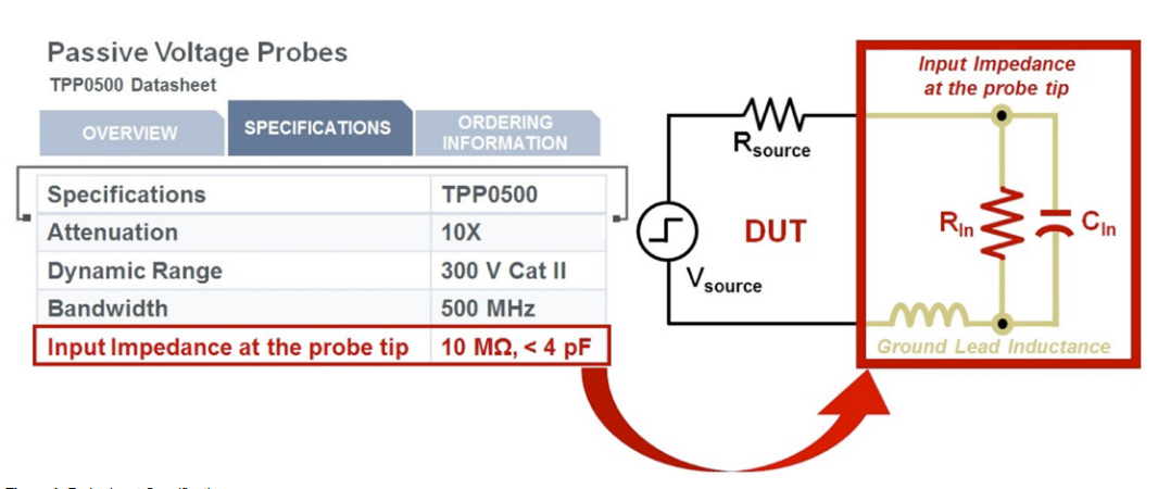
If I soldered a 15 pF capacitor from a random location in your circuit to ground, would you expect the circuit to behavior differently? Of course you would. Because an oscilloscope probe has a capacitance, resistance and inductance, it’s going to affect the signal you’re measuring and can affect the operation of the circuit. To produce a voltage waveform on the oscilloscope, the probe tip is going to draw some current; it’s conductive. Since the probe tip has to draw some current, it’s going to disturb or load the circuit. There are two probe specifications related to the probe loading the circuit, and these loading factors are input resistance and input capacitance. An example of probe input impedance data sheet specifications and an example of how these specifications may be modeled are shown in Figure 1.
Input Resistance Specification
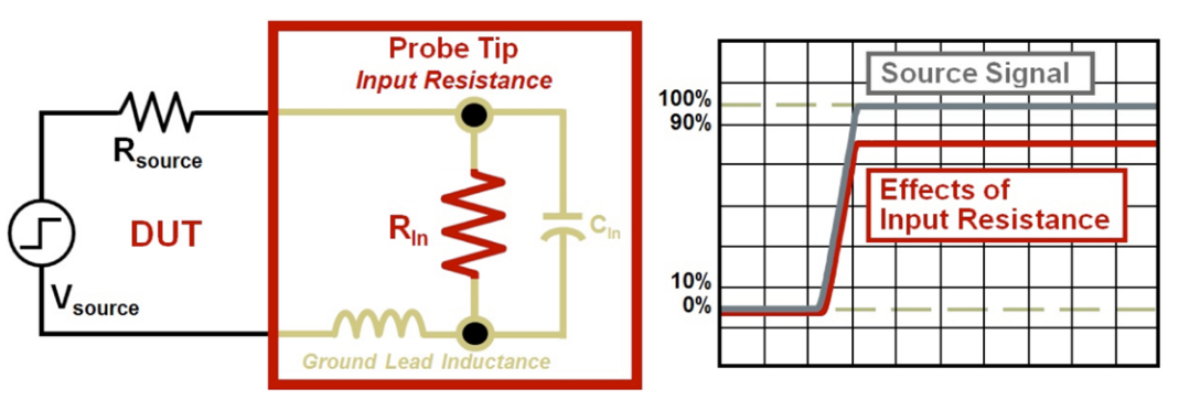
Let’s first investigate the Input Resistance specification. The probe and scope input resistance will reduce the amplitude of the signal under test as shown in waveform on the right of Figure 2. The waveform shape of the loaded signal will closely resemble the source signal, but the amplitude will change. How much the source signal’s amplitude is reduced generally depends on the source resistance because most passive probes that ship with an oscilloscope have a very large 10 MΩ input resistance.
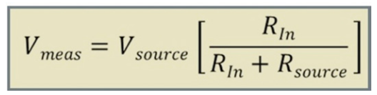
The input resistance of the probe combined with the scope’s input resistance causes the measurement system to act like a voltage divider. The calculation for the effect of input resistance is shown in Equation 1.
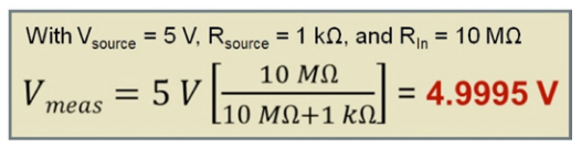
Ideally, Vmeas would equal Vsource because the signal at the test point would be unchanged. In reality, the input resistance of the probe and scope will have some impact on the measured amplitude. To minimize resistive loading, probes typically have a large input resistance, and for most applications, the input resistance of a probe is less likely to cause significant probe loading since most 10X passive probes that ship with an oscilloscope have 10 MΩ input resistance. Equation 2 shows how a system’s large input resistance causes very little loading or disturbance to the circuit.
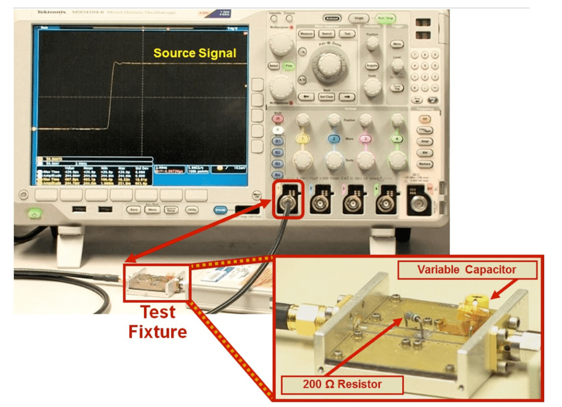
As shown in Equation 2, a measurement system’s large 10 MΩ input resistance has little impact on the measured signal. In this example, the measured signal is calculated at 4.9995 V which is 99.99% of the 5 V source signal. Reviewing equations and models helps provide an academic overview of input resistance, but the best method to see the impact of probe loading is to show how the signal at the test point changes. Figure 3 presents a test setup using a voltage source with 50 Ω source resistance, a test fixture and an oscilloscope. The test fixture has a 200 Ω resistor and variable capacitor soldered to it. You can clearly see the test fixture is directly cabled to the oscilloscope with the output of the test fixture attached to Channel 1. This setup is intended to show what is happening at the test point and to observe the effects of probe loading. The oscilloscope is showing the output of the test fixture, not the output of a probe.
With 10 MΩ, it would be difficult to see the effect of input resistance at the DUT. To see how input resistance affects the signal at the test point, Figure 4 shows the effects of the 200 Ω resistor soldered into the test fixture to exaggerate the effect. The reference waveform is the source signal, and Channel 1 is the source signal loaded by the 200 Ω resistor’s input resistance. Measurements are turned on to observe the amplitude and rise time of both the reference waveform and the loaded waveform. The waveform shape of the loaded waveform is similar to the source signal as is the rise time, but the amplitude has been decreased.
Input Capacitance Specification
When selecting the right probe for their application, most users typically look at the probe’s bandwidth, dynamic range, and perhaps even the input resistance specification. When evaluating a probe’s loading characteristics, most users see the 10 MΩ input resistance value and conclude the probe has sufficient loading capabilities. A critical probe specification almost always overlooked is the probe’s input capacitance. When measuring signals at lower frequencies, the probe’s capacitance has a reactance that is very high, and the probe loading is not as much. However, as the measured signal’s frequency increases, the capacitive reactance decreases. At higher frequencies, the probe’s impedance decreases causing much greater probe loading. The larger the probe’s input capacitance, the more it’s going to disturb or load the circuit when the measured frequency increases.
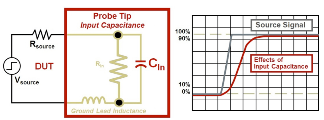
The effect of input capacitance is shown on the waveform on the right of Figure 5. Compared to the source signal, the waveform impacted by a larger input capacitance value has a front corner that is rounded. The consequence of a large capacitance value is severe because the front edge of the signal contains the high frequency content. When this critical signal content has been compromised, one has to question whether measurement results are reliable. When selecting a probe, users need to identify a probing solution with the lowest input capacitance.
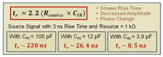
Using the simple model from Figure 5, a first order equation shows that a larger input capacitance will result in significantly slower rise times and lower bandwidth. Based on the rise time calculation in Equation 3, there is a clear relationship between larger input capacitance and slower rise times.
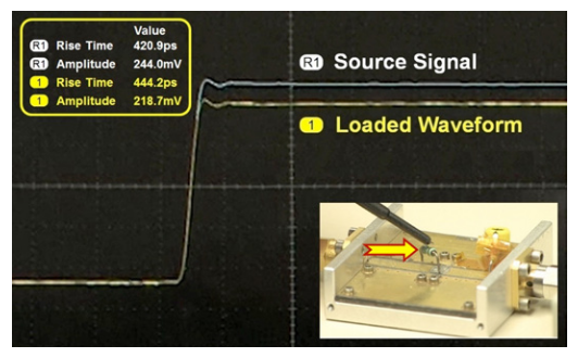
Using the test setup from Figure 3, the variable capacitor soldered into the test fixture will now be connected to the signal strip line to show the effects of probe input capacitance.With the variable capacitor adjusted to 50 pF, the impact of capacitive loading is shown in Figure 6. Again, the source signal is shown as the reference waveform identified as R1 and Channel 1 is the output of the test fixture which is the waveform loaded by the variable capacitor.
Measurements reveal the differences in amplitude and rise between the reference waveform and the loaded waveform.The impact of capacitive loading is obvious. The front edge has been degraded, the rise time is significantly slower, and there is a minor phase shift.
How Does the Passive Probe Shipped with Your Oscilloscope Load Your Signal?
The test setup in the previous sections used simple resistive and capacitive components to isolate the effects of input resistance and input capacitance. Now let’s turn our attention to the impact of input capacitance induced by some passive probes that ship with an oscilloscope.
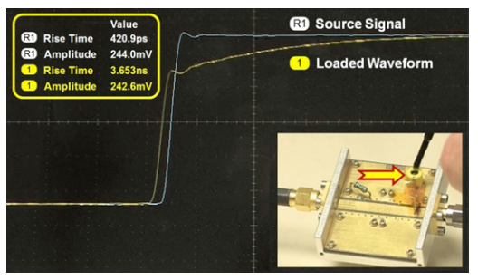
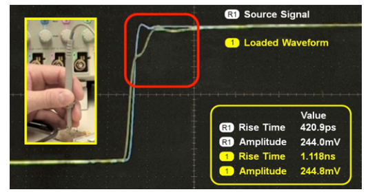
Let’s first examine the loading effects of a passive probe from Agilent which ships standard with the scope. This probe has many of the specifications users are looking for: 500 MHz bandwidth, 300 V CAT II dynamic range, and 10 MΩ input resistance. This probe also has 9.5 pF input capacitance which is comparable with passive probes offered by other vendors. Using the same test setup from Figure 3, the Agilent passive probe will be connected to the test fixture as shown in top left corner of Figure 7. The probe tip is applied to the signal path and a short ground spring is connected to ground. The impact of input capacitance is apparent. The front corner of the loaded waveform in Figure 7 is degraded and the rise time is significantly slower. The signal you’re measuring now looks very little like the original source signal. This degraded signal will be further changed as it travels through the probe cable to the probe’s compensation box and finally to the scope. This test signal has to be reconstructed by the probe and the scope to make it look like the original signal. This kind of loading or disturbance will have adverse effects when you’re performing important circuit validation.
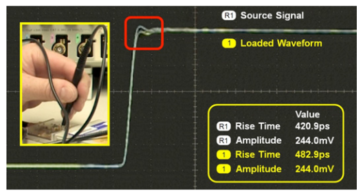
Because of the adverse effects of capacitive loading, Tektronix includes a new series of passive probes with their oscilloscopes with industry best input capacitance of 3.9 pF. These products are the TPP1000, TPP0500B, and TPP0250. Connecting a TPP0500B to the test fixture as shown in Figure 8, the benefits of a probe with low input capacitance are obvious. The signal on Channel 1 which is the loaded waveform is nearly identical to the source signal. Also, the rise time of the loaded waveform is minimally affected. Once again, you want to make measurements with a probe that is going to do less harm, meaning it is only going to minimally affect the signal you’re measuring. A low capacitance passive probe from Tektronix offers nearly the probe loading benefits of an active probe.
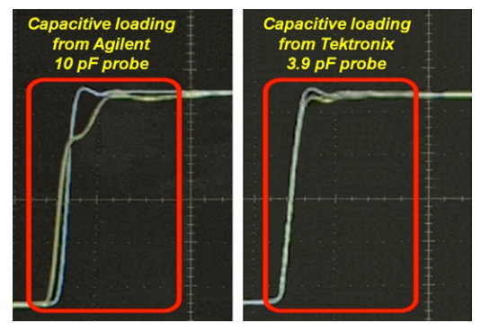
Figure 9 compares the capacitive loading of an Agilent standard probe against the Tektronix TPP0500B. The differences are dramatic. In today’s world, signals have faster edges and tighter margins, so the designer has to make the effort to model, run simulations, and validate the design. When you spend that much time and effort in the design process, you don’t want to second-guess the measurement system or spend additional time troubleshooting due to measurement inaccuracy. In this case, one would have to question if the effects of probe loading are the weak link in validating the design.
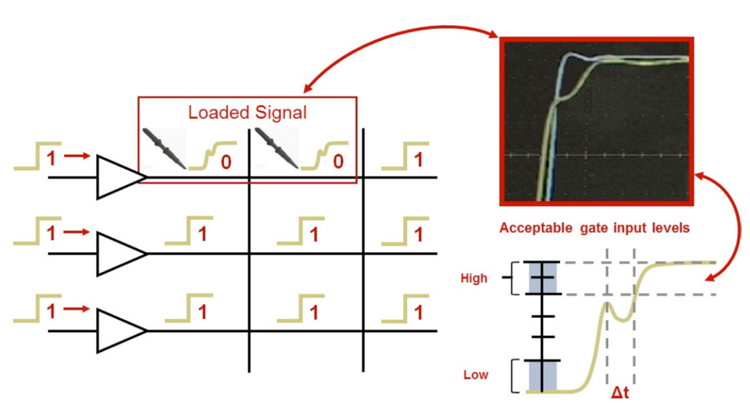
A probe’s loading affect may not only cause measurement inaccuracy but can also affect circuit operation. In the example shown in Figure 10, the probe’s large input capacitance has caused the signal to fail to meet critical setup and hold time requirements. You can also see how a degraded front edge or ringing can cause reflections which will compromise signal fidelity. When you’re validating your design, the last thing you want to do is fight the test equipment. It is critical to select a probe which is going to cause less disturbance by selecting a probe with low input capacitance.
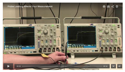
How Probe Loading Affects Your Measurement
The video shows a comparison of what is occurring at the test point and what the output of the probe looks like Click here.
Conclusion
When selecting a probe, users will first look at what are considered to be the banner specifications which are bandwidth and dynamic range. A more knowledgeable user may even check the input resistance to make sure it’s a large value. However, a critical specification often overlooked is the probe’s input capacitance. It is important to use a probe with a smaller input capacitance because it is going to cause less disturbance or loading.
You may be using a probe with a larger input capacitance and you’re getting the results you want. The question is, are those results real and reliable? There may be more going on at the test point than you considered and just because the probe reconstructs a signal you’re expecting to see doesn’t mean your results are accurate. Using a probe with a smaller input capacitance will cause less disturbance or loading at the test point, which greatly increases the likelihood you’ll get a measurement with greater accuracy
Find more valuable resources at TEK.COM
Copyright © Tektronix. All rights reserved. Tektronix products are covered by U.S. and foreign patents, issued and pending. Information in this publication supersedes that in all previously published material. Specification and price change privileges reserved. TEKTRONIX and TEK are registered trademarks of Tektronix, Inc. All other trade names referenced are the service marks, trademarks or registered trademarks of their respective companies.
01/14 51W-30013-0