
Contact us
Live Chat with Tek representatives. Available 6:00 AM - 4:30 PM
Call
Call us at
Available 6:00 AM – 5:00 PM (PST) Business Days
Download
Download Manuals, Datasheets, Software and more:
Feedback
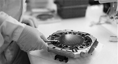
Material Science
Unlocking the Potential of New Materials
Today’s consumers are demanding smaller, lighter, cheaper, and more capable electronics than ever before with ever-longer operating times. To address these conflicting demands, researchers need to develop new materials, miniaturize existing devices, and enhance device efficiencies. The effort to boost device density and performance while reducing power consumption has led to research into graphene and other two-dimensional (2-D) solids with high carrier mobility, as well as organic semiconductors and nano-scale devices.
High efficiency batteries based on new electrolyte and electrode materials will be critical to extending operating times. Advanced fuel cell technologies designed to make the next generation of electric vehicles more efficient and affordable are also under investigation. The desire for greener power generation solutions is spurring investigation into higher temperature superconductors and the power semiconductors essential to power conversion. Materials like gallium arsenide (GaAs) and silicon carbide (SiC) will be crucial to future power transmission technologies. Materials research is also central to boosting the conversion efficiency and power output of solar cells. Boosting the efficiency of laser diodes to increase data transmission capacity requires studying new materials and structures.
Ultra-sensitive measurements are central to materials characterization, from measuring femtoamp-level leakage currents to micro-ohm-level resistance measurements for assessing the resistivity of high carrier mobility materials. On the other end of the scale, characterizing the latest insulators often entails teraohm measurements. Superconductor or nanomaterials research performed at near 0⁰K requires reducing the level of power applied to prevent self-heating, which can affect the device’s or material’s response or damage it. That calls for sourcing very low DC currents or current pulses.
Featured Content
Recommended Equipment
Ultra-Low Resistance Configurations
4200A-SCS Parameter Analyzer

Series 6400 Picoammeters

6430 Electrometer

Graphical Touchscreen SourceMeter® Source Measure Unit (SMU) Instruments

Keithey Potentiostats for ElectroChemistry
