Introduction
Extensive research and development have been invested in semiconductor-based biosensors because of their low cost, rapid response, and accurate detection. In particular, field effect transistor (FET) based biosensors, or bioFETs, are used in a wide variety of applications such as in biological research, point-of-care diagnostics, environmental applications and even in food safety.
A bioFET converts a biological response to an analyte and converts it into an electrical signal that can be easily measured using DC I-V techniques. The output characteristics (Id-Vd), transfer (Id-Vg) characteristics, and current measurements vs.time (I-t) can be related to the detection and magnitude of the analyte.
These DC I-V tests can easily be measured using multiple Source Measure Units (SMUs) depending on the number of terminals on the device. An SMU is an instrument that can source and measure current and voltage and can be used to apply voltage to the gate and drain terminals of the FET. An integrated system that combines multiple SMUs with interactive software is the Keithley 4200A-SCS Parameter Analyzer shown in Figure 1. This configurable test system simplifies these measurements into one integrated system that includes hardware, interactive software, graphics, and analysis capabilities.
This application note describes typical bioFETs, explains how to make electrical connections from the SMUs to the device, defines common DC I-V tests and the instruments used to make the measurements, and explains measurement considerations for optimal results.

The BioFET Sensor
The bioFET combines a transistor with a bio-sensitive layer that can detect a biological component such as bio-molecules.A simplified diagram illustrating how a bioFET works is shown in Figure 2.
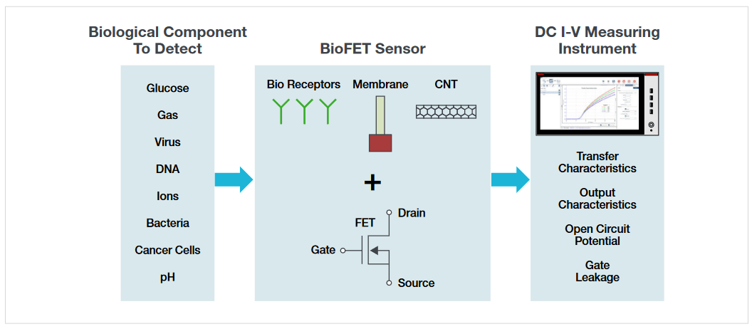
Using a bioFET, biological components such as glucose, a virus, PH, or cancer cells are detected by a sensing element such as bio receptors, a sensing membrane, or carbon nanomaterial that are part of the bioFET. The device converts the biological response to an analyte into an electrical signal. The detection and concentration of the biological element is related to the drain current flowing through the transistor. The electrical signal of the FET is then measured using DC I-V measuring instruments. These are the same measuring instruments that are used to measure traditional transistors.
Common DC I-V tests that are performed on these devices include the transfer characteristics, output characteristics, threshold voltage, open circuit potential, and the gate leakage current of the device.
MOSFET Overview
Many bioFET sensors are based on a MOSFET, or MetalOxide-Semiconductor FET, which is a three or four terminal FET with an insulated gate.
Figure 3 shows an n-channel MOSFET, or an nMOS transistor, with four terminals: the gate, drain, source and bulk. The source and drain contacts are heavily doped n+ areas. The substrate is a low doped material, p-. The gate is insulated from the channel with a very thin oxide layer often SiO2.
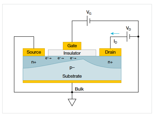
When voltage sources are connected to the gate and drain terminals and bias voltages, Vg and Vd, are applied, a conductive channel is formed between the source and drain terminals. Current begins to flow from the drain to the source. The direction of the current flow is opposite to the direction of movement of the negatively charged electrons. The gate voltage controls the channel along with the charge carriers.
As shown in Figure 4, the two power supplies in the circuit can be replaced with SMUs which can source voltage and measure current for determining the I-V characteristics of the MOSFET. In this example, one SMU is connected to the gate terminal and applies the gate voltage and measures the gate leakage current. A second SMU is connected to the drain terminal and forces the drain voltage and measures the resulting drain current.
Besides forcing voltage and measuring current, the SMU can remotely change the polarity of the voltage source and set a compliance current to prevent excessive current from damaging the device.
Depending on the desired I-V measurements, SMUs can also be connected to the Source and Bulk terminals of the MOSFET. However, in this example, the source and bulk terminals are connected to the LO terminals of the SMUs.
When using multiple SMUs, the timing of the SMUs must be synchronized which is done automatically within the 4200A-SCS Parameter Analyzer.
The bioFET combines a transistor with a bio-sensitive layer that can detect a biological component such as bio-molecules.A simplified diagram illustrating how a bioFET works is shown in Figure 2.

Example BioFETs
In this section, examples of common bioFETs and how electrical connections are made to these devices will be provided. These examples include a back-gated bioFET, an extended-gate FET, and an ion-sensitive FET.
Back-Gated BioFET
In the back-gated bioFET, shown in Figure 5, an electrically and chemically insulating material separates the semiconductor layer from the conducting channel. When the bio receptor is exposed to a particular analyte or biological element, the I-V characteristics of the FET will be affected. In this case, the drain current is related to a biological factor, such as a pathogen, or other biological analyte.
The two SMUs in the circuit are used to bias and characterize the device. One SMU is connected to the gate and a second SMU is connected to the drain. The source terminal can be connected to the ground unit of the 4200A-SCS or to a third SMU.
In this example, SMU1 supplies the gate voltage and can also be used to measure the gate leakage current. Sometimes a power supply is used to force the gate voltage, but using an SMU provides an advantage because it can also measure the gate leakage current which is helpful when studying the I-V characteristics of the device. The gate voltage is used to control the channel width and can be used to increase the sensitivity to the analyte so it’s easier to measure the drain current. SMU2 is connected to the drain terminal and forces the drain voltage (VD) and measures the drain current (ID).

Extended-Gate FET (EGFET)
Figure 6 shows an extended-gate FET which includes both a sensing structure and a MOSFET. In this bioFET, the sensing structure and the MOSFET are physically separated into two parts. Because the MOSFET is separate from the sensing element, a commercially available MOSFET can be used as the transducer.
The EGFET has a working electrode that is in direct contact to the gate of the MOSFET. The working electrode also has a sensing membrane in an electrolyte solution which is used to sense the analyte. In this configuration, SMU1 is connected to the reference electrode and forces the reference voltage (VREF). This voltage is used to control the channel width of the FET. SMU2 forces the drain voltage (VD) and measures the drain current (ID).
Like the back-gated FET, the transfer characteristics (ID vs.VREF) of the MOSFET measured by the two SMUs will change depending on the analyte. The SMUs can also be used to measure the output characteristics (ID vs.VD) and the gate leakage current of the device.
Some applications for EGFETs include detecting specific molecules such as glucose, pH, and ion species.

Ion-Sensitive FET (ISFET)
Shown in Figure 7, the ion-sensitive field effect transistor (ISFET) is used to measure the ion concentration in a solution. The ion concentration is related to the drain current flowing through the transistor. ISFETs are used in a wide range of biomedical applications such as pH monitoring, glucose measurements, and antibody detection.
The ion-sensitive FET, like the EGFET, has both a sensing structure and a MOSFET. However, unlike the EGFET, the sensing element and the FET are not physically separated but are combined. The ISFET has the same basic structure of a MOSFET including a gate, drain, and source. However, the metal gate of the traditional MOSFET is replaced by a reference electrode in a solution and an ion-sensitive membrane. This example shows a silicon channel, but the channel can also be made of other materials such as graphene, silicon nanowires, or carbon nanotubes.
In this example, the Reference Electrode is connected to SMU1 which forces voltage and measure the gate current. The gate voltage is applied between the reference electrode and the substrate and forms an inversion layer between the drain and source terminals of the FET. The drain of the FET is connected to SMU2 which forces the drain voltage and measures the drain current. The back contact is used to connect the substrate of the ISFET to the Force LO terminal of the GNDU. When the ion concentration of the electrolyte solution changes the drain current of the FET also changes and is measured by SMU2.

DC I-V Measurements
This section will describe common DC I-V measurements used to characterize bioFETs include the transfer characteristics (IdVg), output characteristics (Id-Vd) and drain current vs. time measurements (Id-t).
Transfer Characteristics (Id-Vg)
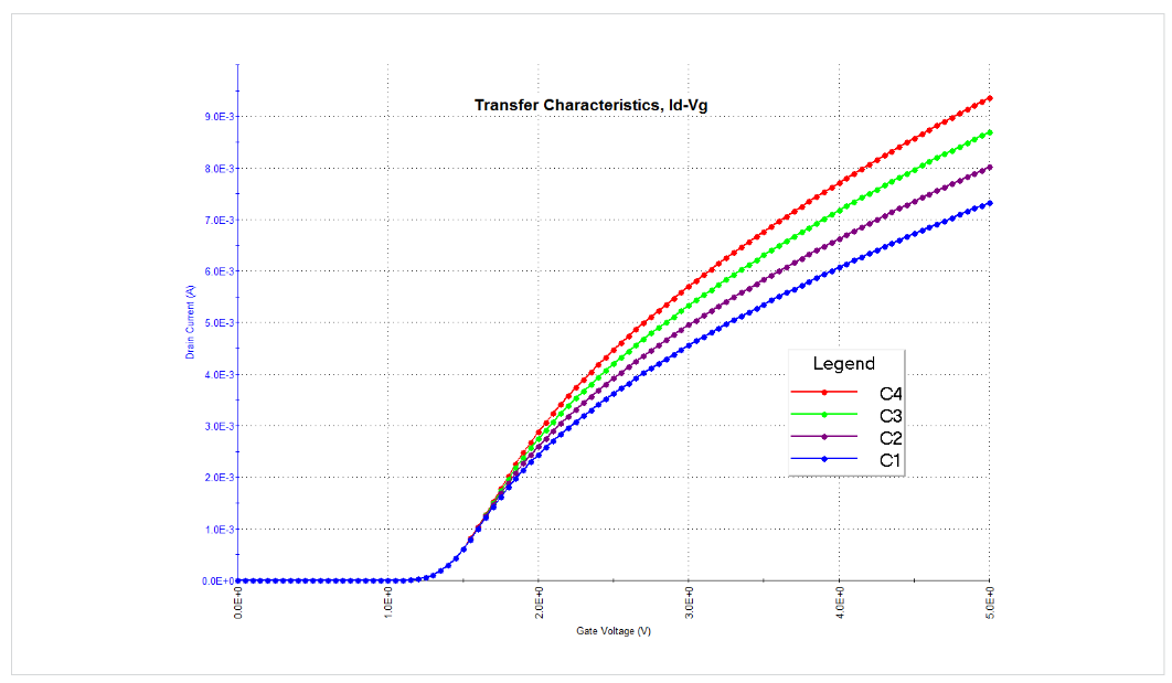
Probably the most common electrical measurement on the bioFET is the transfer characteristics which plots the drain current vs.the gate voltage. The transfer characteristics are usually related to the concentration of a pathogen or other biological factor that’s being investigated.
In this test, one SMU sweeps the gate voltage and a second SMU measures the resulting drain current at a constant drain voltage. Figure 8 shows four different curves which represent four different concentrations of the pathogen. These curves were generated using the 4200A-SCS Parameter Analyzer.
The Library in the Clarius software comes with a test that performs the transfer characteristics of a FET as well as a project that has tests for both the transfer and output characteristics. These tests and project can be found by entering biofet in the search bar of the Library in the Select view of the software. A screen capture of the Configure view of this test is shown in Figure 9.

Output Characteristics (Id-Vd)
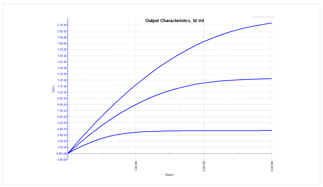
Another common test is determining the output characteristics, which is the drain current as a function of drain voltage, of the FET as shown in Figure 10. These curves were generated using two SMUs in the 4200A-SCS Parameter Analyzer.
In this case, SMU1, which is connected to the gate, steps a voltage, while SMU2, connected to the drain, sweeps the voltage and measures the resulting current.
To test the functionality of the FET, multiple gate steps enables the generation of a family of curves and shows the dependency of the drain current on the gate voltage. Alternatively, the gate voltage can be kept constant, but changes to the biological component are made to observe how different components or concentrations affect the drain current.
Drain Current vs. Time (Id-t)
The dynamic response of a bioFET sensor can be monitored by graphing the drain current as a function of time as shown in Figure 11. The magnitude of the drain current will change as the concentration of the analyte changes.
In this application, both the gate and drain voltage biases remain constant as the drain current is measured so that only the analyte is changing.

Measurement Optimization
In this section, ways to achieve optimal measurements including running a blank or empty test, minimizing noisy readings, allowing sufficient settling time, and using compliance to avoid damaging devices will be described.
Run a “blank” test: Once the system is set up, it’s a good idea to run a “blank”, or empty, test to make sure everything is set up and configured properly. This test will establish a baseline current by measuring the I-V characteristics of the device to make sure it is working properly without any biological component added. Adjustments can be made to the test circuit and settings, as necessary, prior to adding the biological component. Depending on the type of device, this may or may not be possible to do.
Minimize noisy readings: Noisy measurements are probably one of the most common problems when measuring low current. The drain current or gate leakage current of the bioFET can be in the nanoamp and picoamp range. Noisy readings can be caused by several reasons and may take some experimenting to determine the source.
Electrostatic interference occurs when an electrically charged object approaches the circuit under test. In high impedance circuits, this charge doesn’t decay rapidly and can result in unstable measurements. The erroneous readings may be due to either DC or AC electrostatic fields, so electrostatic shielding will help minimize the effects of these fields.
The electrostatic shield can be just a simple metal box that encloses the test circuit. Probe stations often include an electrostatic/EMI shield or optional dark box. The shield should be connected to the measurement circuit LO, which is the Force LO terminal of the SMU. The Force LO terminal is the outside shield of the triax cable of the SMU or is located on the GNDU. All cables need to be of a low noise design and shielded. Each 42XX-SMU comes with two low-noise triax cables.
Another way to reduce noise is to control external noise sources. These noise sources are interferences created by motors, computer screens, or other electrical equipment in or near the lab or test station. They can be controlled by shielding and filtering or by removing or turning off the noise source.
In summary, to minimize noisy readings:
- Keep all charged objects, including people, and conductors away from the sensitive areas of the test circuit.
- Avoid movement and vibration near the test area.
- Control or remove external noise sources.
- Increase the integration time of the measurement which can be adjusted using the Custom Speed mode in the Test Settings window in Clarius.
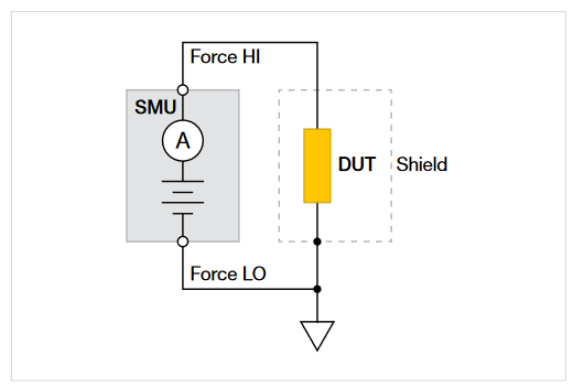
- Shield the device under test by surrounding it with a conductive enclosure and connect the enclosure electrically to the test circuit common terminal (Force LO) as shown in Figure 12. The shield can be just a simple metal box or meshed screen that encloses the test circuit.
Limit Current: To prevent damage to the device while performing I-V characterization, set the compliance to limit the amount of current that can flow through the device. This can be done in the Clarius software by setting the current compliance of each SMU to a safe level. This is a programmed limit to ensure the current doesn’t exceed the user-defined level.
Provide sufficient settling time: When measuring low current (<1 µA), it is important to allow sufficient settling time to ensure the measurements are stabilized after a current or voltage has been applied or changed such as when the gate voltage is sweeping and measuring the drain current. Factors affecting the settling time of the circuit include the shunt capacitance of the test circuit and the device resistance. The shunt capacitance includes the cables, test fixtures, probers, and switch matrices.
The settling time of the measurement circuit can be determined by plotting the current vs.time to a stepped voltage. The settling time can be visually determined by the graph. Once the settling time is determined, this value can be used as the voltage sweep delay time in the Test Settings window of the Clarius software.
Conclusion
Research and development of FET-based biosensors have increased because of their low cost, rapid response, and accurate detection. A bioFET converts a biological response to an analyte into an electrical signal that can easily by measured by DC I-V instrumentation. SMUs in the 4200A-SCS Parameter Analyzer are used to perform the I-V characterization of bioFETs. Using the appropriate instrument settings and applying proper measurement techniques will lead to optimal measurement results.
Further information on making optimal low current measurements can be found in the Keithley Low Level Measurements Handbook, which can be downloaded from the Tek.com website.
Find more valuable resources at TEK.COM
Copyright © Tektronix. All rights reserved. Tektronix products are covered by U.S. and foreign patents, issued and pending. Information in this publication supersedes that in all previously published material. Specification and price change privileges reserved. TEKTRONIX and TEK are registered trademarks of Tektronix, Inc. All other trade names referenced are the service marks, trademarks or registered trademarks of their respective companies.
102620 1KW-73757