Debug Your FPGA Design at Full Speed
Solutions such as mixed signal oscilloscopes (MSOs) and logic analyzers with FPGAView™ enable you to instantly move probe points within your Xilinx and Altera FPGAs without the need to recompile your design. Plus the ability to correlate internal FPGA signal activity to board-level signals can make the difference between hitting your schedule and missing your time-to-market window.
Introduction
The phenomenal growth in design size and complexity continues to make the process of design verification a critical bottleneck for systems based on Field Programmable Gate Arrays (FPGAs). Limited access to internal signals, advanced FPGA packages, and printed circuit board (PCB) electrical noise are all contributing factors in making design debug and verification the most difficult process of the design cycle.You can easily spend the majority of your design cycle time debugging and verifying your design. To help you with the process of design debug and verification, new tools are required to help debug your design while it is running at full speed on your FPGA.
This application note focuses on the issues and techniques that can help you become more efficient when debugging your FPGA systems.
FPGA Design Process Overview
There are two distinct phases in bringing an FPGA system to market: the Design Phase and the Debug and Verification Phase (See Figure 1). The primary tasks in the Design Phase are entry, simulation, and implementation. The primary tasks in the Debug and Verification Phase are to validate the design and correct any bugs found.
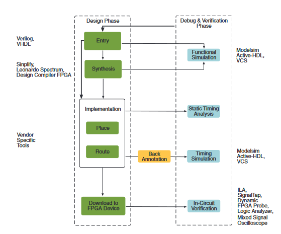
The Design Phase
Not only is the design captured in this phase, but debugging begins with the use of simulation tools. The proper use of simulation has proven to be an effective way of finding and correcting many design errors. However, simulation should not be relied upon as the only tool to debug a FPGA design. There are too many things that simulation just can not catch.In the Design Phase you also need to look ahead to the Debug and Verification Phase and plan how you will debug your FPGA in-circuit and at-speed. This should lead you to define the overall debug approach, help identify any test and measurement tools required, and identify any impact that the chosen debug method has on the design of the board.
The Debug and Verification Phase
During the Debug Phase, you need to find the hard problems that were not caught by simulation. Doing this in a timeeffective way is the challenge.In this application note, we will look at how to select the proper FPGA debug methodology, how to effectively plan for debug during the design phase, and how to harness the power of new methodologies that allow you see many internal FPGA signals using just a few FPGA pins. Done properly, this will allow you to breakthrough your most difficult FPGA debug problems.
FPGA Debug Methodologies
The key choice that needs to be made in the design phase is which FPGA debug methodology to use. Ideally, you want a methodology that is portable to all of your FPGA designs, provides you insight into both your FPGA operation and your system operation, and gives you the power to pinpoint and analyze difficult problems.
There are two basic in-circuit FPGA debug methodologies: the use of an embedded logic analyzer and the use of external test equipment, such as a mixed signal oscilloscope or logic analyzer. The choice of which methodology to use depends on the debug needs of your project.
Embedded Logic Analyzer Core
The major FPGA vendors offer embedded logic analyzer cores. Examples include SignalTap® II from Altera and ChipScope™ ILA from Xilinx. These intellectual property blocks are inserted into your FPGA design and provide both triggering capability and storage capability. FPGA logic resources are used to implement the trigger circuit and FPGA memory blocks are used to implement the storage capability. JTAG is used to configure the operation of the core and is used to pass the captured data to a PC for viewing.
Because the embedded logic analyzer uses internal FPGA resources, they are most often used with larger FPGAs that can better absorb the overhead of the core. Typically you want the core to take up no more than 5% of the available FPGA logic resources.
As with any debug methodology, there are some trade-offs that you should be aware of:
Pins vs. Internal Resources
Embedded logic analyzer cores use no additional pins since they are accessed via the existing JTAG pins. This means that you can use this method even if your design is pinconstrained. The trade-off is that you use internal FPGA logic resources and memory blocks that could be used to implement your design. Also, since internal memory is used to capture the data, memory depths tend to be relatively shallow.
Probing vs. Operating Mode
The probing for an embedded logic analyzer core is simple.It uses the existing JTAG pins, so you do not need to worry about how to connect an external logic analyzer to your system. The trade-off is that while the embedded logic analyzer gives you visibility into the operation of your FPGA, you do not have a way of correlating that information to boardlevel or system-level information. The correlation of signals inside the FPGA with those outside of the FPGA is often critical to solving the toughest of debug challenges.
Cost vs. Flexibility
Most FPGA vendors offer their embedded logic analyzer cores for less than the cost of a full-functional external logic analyzer.As you would expect though, embedded logic analyzer cores offer less functionality than a full-function logic analyzer – functionality that is often needed to capture and analyzer your tough debug challenges. For example, embedded logic analyzers can only operate in state mode – they capture data synchronous to a specified clock that is present in your FPGA design and therefore can not provide accurate signal timing relationships.
External Test Equipment
Because of some of the limitations of the embedded logic analyzer methodology, many FPGA designers have adopted a methodology that uses the flexibility of the FPGA and the power of an external mixed signal oscilloscope such as the MSO5000, MSO4000, MSO3000, or MSO2000 Series, or logic analyzer such as the TLA Series.
In this methodology, internal signals of interest are routed to unused pins of the FPGA, which are then connected to the external test equipment. This approach leverages the very deep acquisition memory in the external test equipment, which is useful when debugging problems where the symptom and the actual cause are separated by a large amount of time. It also offers the ability to correlate the internal FPGA signals with other activity in the system.
As with the embedded logic analyzer methodology, there are trade-offs to consider:
Pins vs. Internal Resources
The external test equipment approach uses very few (if any) logic resources and no FPGA memory. This frees these resources to IMPLEMENT your functionality. The trade-off is now that you need to dedicate some number of incremental pins for debug. These are, obviously, pins that could have been used by your design.
Probing vs. Operating Mode
The probe connections to the external test equipment is a little more involved than the probing required for the embedded logic analyzer approach. Rather than being able to reuse the JTAG connector that is already on your board, you need to determine how to access your FPGA signal with the MSO or logic analyzer probes. The easiest technique is to add a debug connector to your board. This will also enable you to easily correlate your FPGA signals with other signals in the system.
Cost vs. Flexibility
While it is true that external test equipment may have a higher initial cost than an embedded logic analyzer, you can also solve a wider range of problems with it. Not only is the MSO or logic analyzer useful for FPGA debug, it can be used to solve your other digital and mixed signal design challenges. You also get more flexibility in acquisition modes and trigger capability.With an external MSO, you have the ability to trigger on and capture a wide variety of analog, digital, and serial signals with very high timing resolution. With an external logic analyzer, you have access to as many as 16 different trigger states and can capture very long buffers of data in timing mode with very high timing resolution.
Selecting the Appropriate FPGA Debug Methodology
Both methodologies can be useful depending on your situation. The challege is to determine which approach is appropriate for your design. Ask yourself the following questions:
What are the anticipated problems?
If you think they will be isolated to functional problems within the FPGA, the use of an embedded logic analyzer may be all the debug capability that is required. If, however, you anticipate larger debug problems that require you to verify timing margins, correlate internal FPGA activity with other activity on your board, or require more powerful triggering capability, the use of external test equipment is more suited to your debug needs.
Will you have a need to look at at-speed timing information in addition to just state data?
An external MSO or logic analyzer allows you to see the detailed timing relationships of your FPGA signals with resolution much less than a nanosecond. This helps verify that events are really happening as they are designed to and allows you to verify the timing margins of your design. An embedded logic analyzer can only capture data synchronous to a specified clock that is present in your FPGA.
How deep of a capture will you need?
You will have access to a greater sample depth with an external MSO or logic analyzer. In SignalTap II for instance, the maximum sample depth is set to 128 Kb, which is a device constraint. However, with an external MSO you can capture up to 40M samples, and with a logic analyzer you will be able to capture up to 256M samples. This can help you see more of the problem and its potential cause, thus shortening your debug time.
Are you more pin-constrained or resourceconstrained in your design?
Using an embedded logic analyzer requires no additional output pins but internal FPGA resources must be used to implement the logic analyzer functions. Using external test equipment requires the use of additional output pins but minimizes (or eliminates) the need to use internal FPGA resources.
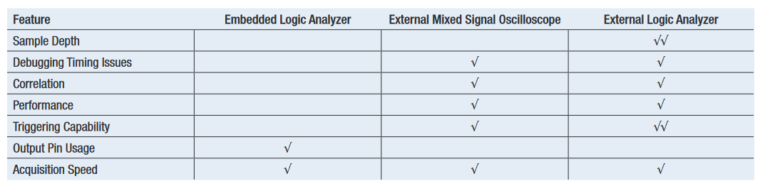
Table 1 summarizes the relative strengths of each approach.
The FPGAView™ Advantage
Overview of FPGAView
The external test equipment method makes effective use of the "P" in FPGA to reprogram the device as needed to route the internal signals of interest to what is typically a small number of pins. This is a very useful approach but it does have limitations:
- Every time you need to look at a different set of internal signals, you need to change your design (either at the RTL-level or using an FPGA editor tool) to route the desired set of signals to the debug pins. This is not only timeconsuming but, if it requires a re-compile of the design, can change the timing of the design and potentially hide the problem you need to solve.
- Typically there are a small number of debug pins and the 1:1 relationship between internal signals and debug pins limits visibility and insight into the design.
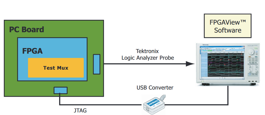
To overcome these limitations, a method of FPGA debug has been created that delivers all of the advantages of the external test equipment approach while removing its primary limitations. FPGAView, used with a Tektronix MSO5000/4000/3000/2000 Series mixed signal oscilloscope or TLA Series logic analyzer, provides a complete solution for debugging your Xilinx and Altera FPGAs and surrounding hardware (See Figure 2). This combination allows you to:
- View internal activity and external activity simultaneously
- Quickly change your FPGA probe points without recompiling your design
- Monitor multiple internal FPGA signals per pin
In addition, FPGAView can handle multiple test cores in a single device (useful for monitoring different clock domains) and multiple FPGA devices on a JTAG chain.
Using FPGAView
Using FPGAView consists of these easy steps:
- Step 1. Configure and insert the appropriate test core into your FPGA design
- Step 2. Configure FPGAView to match your debug environment
- Step 3. Establish the mapping of FPGA pins to MSO or TLA logic analyzer channels
- Step 4. Make your measurement
Each of these steps is described in more detail in the following sections.
Step 1. Insert Core
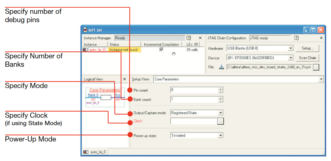
The first step is to configure the test core and insert it into your design. For example, when using Altera devices, you use Altera’s Logic Analyzer Interface Editor to create a test core that best suits your need (See Figure 3a). The On-Chip Instrumentation Generator (OCIGEN) is used to specify and insert a test core into Xilinx devices (See Figure 3b).
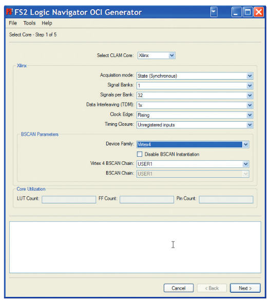
With most test cores you can specify the following parameters:
- Pin Count: Signifies the number of pins you want dedicated to your external test equipment interface.
- Bank Count: Signifies the number of internal signals that you want to map to each pin.
- Output/Capture Mode: Selects the type of acquisition you want to perform. You can select Combination/Timing or Registered/State.
- Clock: If you selected a capture mode of Registered/State, this allows you to select the sample clock for the test core.
After selecting the appropriate parameters for your debug requirements, you need to select which pins will be used by the test core for output. You will also need to select which signals are to be probed and groups those signals into banks.
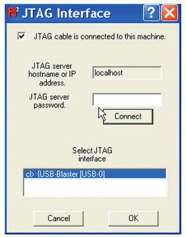
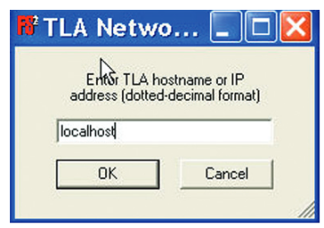
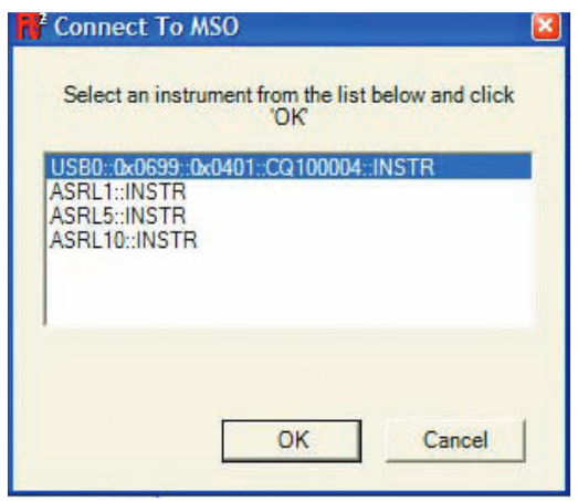
Step 2. Configure FPGAView to match your debug environment
From the FPGAView window, you establish the connection to the JTAG programming cable (See Figure 4) as well as connecting to the external test equipment. Figure 5a and 5b show the connection to the TLA Series logic analyzer, MSO5000/4000/3000/2000 Series oscilloscope, or PC workstation. These configurations provide you with the flexibility needed to match your debug challenges.
Step 3. Map FPGA Pins to Mixed Signal Oscilloscope or Logic Analyzer
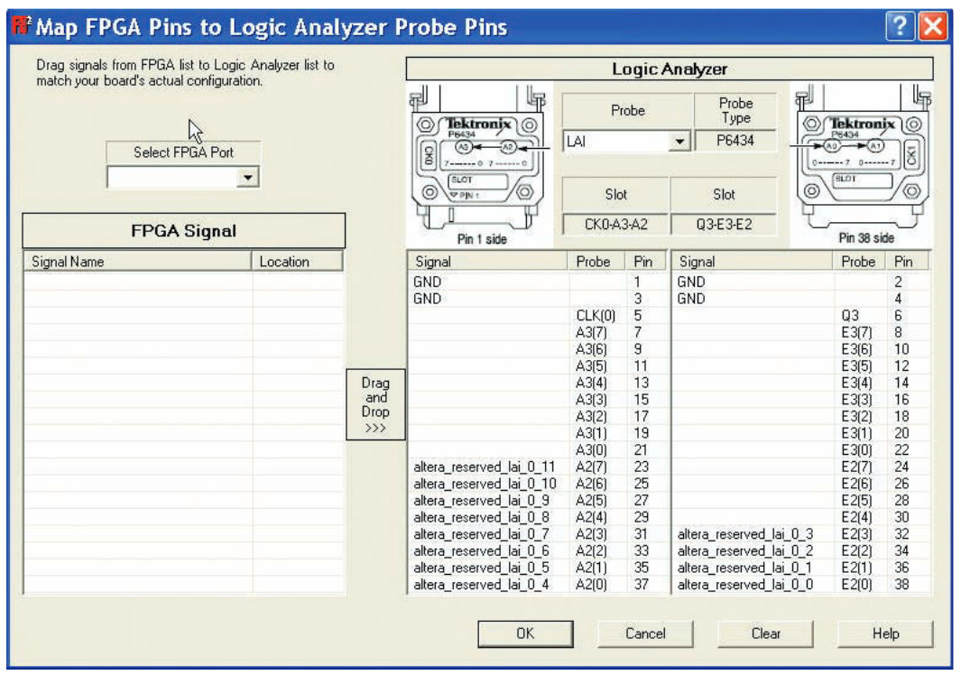
The next step is to map the physical connection between the FPGA pins and the mixed signal oscilloscope or TLA Series logic analyzer. This will allow FPGAView to automatically update the signal names displayed on the MSO or logic analyzer to match those of the signals in the FPGA design currently being monitored by the test core.
To do this, simply click on the Probes button to bring up a drag-and-drop window for connecting the test core output signal names with the correct channels on the logic analyzer (See Figure 6). This assignment process is only necessary once for a given target connection.
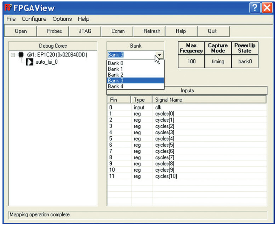
Step 4. Make Your Measurement
The Bank list pull-down lets you select which Bank you want to measure. Once the Bank is selected, FPGAView communicates to your FPGA via the JTAG interface and configures the test core so that the desired Bank is selected.
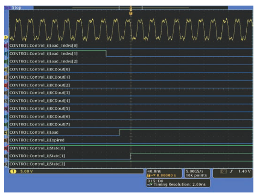
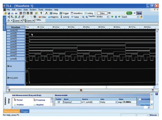
FPGAView also programs the MSO5000/4000/3000/2000 Series mixed signal oscilloscope or TLA Series logic analyzer with these names into the assigned channels making it easy to interpret your measurement results. To measure a different set of internal signals, you simply choose a different bank of signals (See Figure 7). Correlating these FPGA signals with other signals in your system is done automatically by a fullfeatured MSO (See Figure 8a) or TLA Series logic analyzer (See Figure 8b).
Summary
By carefully considering your debug needs during the design phase, you will be able to select the appropriate debug methodology that will both simplify the process and help save you time. The embedded logic analyzer and external test equipment approaches have their own strengths and weaknesses, but new methods such as FPGAView make the external test equipment approach even more appealing.The ability to instantly move probe points without the need to recompile your design and the ability to correlate internal FPGA signal activity to board-level signals can make the difference between hitting your schedule and missing your time-to-market window.