Introduction
As more standards documents of high-speed serial data specify jitter limits, precise and repeatable timing measure- ments are becoming increasingly important and critical. Jitter budgets are becoming tighter, and jitter induced impairments are often the major factor limiting system performance or preventing interoperability.
Designers of next-generation telecom and datacom hardware have been confronted with inherent limitations of measurement instrumentation. While standard instru- ment trigger jitter in Tektronix high-bandwidth sampling oscilloscopes has been improved in recent years to an industry-leading <750fsRMS , many R&D and manufacturing test engineers working on 40 Gigabit systems or high precision Rj/Dj jitter characterization at 10 Gigabit require the lowest possible jitter noise floor in their test instrumentation.
Tektronix responded to these demands by introducing the new CSA8200 Sampling Oscilloscope platform in combination with the 82A04 Phase Reference module which enables ultralow <200fsRMS jitter floor measurements, highest acquisition rate, highest signal fidelity and features uniquely flexible operation modes.
The CSA8200 with the 82A04 module features two new phase-corrected timebase modes. The Triggered Phase Reference mode retains the full functionality and behavior of a sampling oscilloscope. The oscilloscope can be operated just like in the familiar standard timebase mode, and enables the user for example to display specific bits in a single waveform. With the clock phase information provided by the 82A04, the instr ument jitter is now reduced to <200fsRMS.
In addition to the Triggered mode the 82A04 module also offers the Free-Run Phase-Reference mode which has slightly limited functionality and different timebase behavior compared to a typical triggered timebase; its advantage is that is does not need a trigger signal.
Principle of Operation
The phase reference timebase employs a horizontal sample placement method based on phase measur ement against a co-sampled external reference clock signal. Clock phase demodulation is a concept with long history. In fact, the Tektronix TDS8000 Series of sampling oscilloscopes has been utilizesing phase measurements relative to the cycles of an internal SAW oscillator running at 360 MHz to generate the standard timebase. The 82A04 takes this concept a step fur ther by accepting a user supplied external reference oscillator synchronous to the data signal.
This opens up the possibility of allowing significantly higher clock frequencies (by more than two orders of magnitude) and of using highly stable, low phase-noise reference oscillators generated by exter nal clock sources such as stand-alone RF synthesizers, thus resulting in significant timing accuracy improvement over the standard internal timebase.
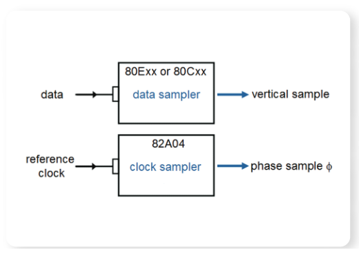
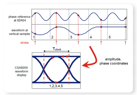
The schematic diagram of a phase-ref acquisition is shown in Figure 1. In the Free-Run mode the oscilloscope does not access its inter nal timebase. Rather, the function of the Phase-Ref module is to extract the relative phase angle of the clock signal and assign it to each vertical data sample taken simultaneously. The data signal is acquired by either an electrical 80E0x or optical 80Cxx plug-in module
The synchronous clock signal is applied to the input of the Phase-Reference module, where a clock sampler measures the clock voltage and determines its relative phase from 0 to 2π. The oscilloscope then builds the waveform display by plotting the vertical data sample on the vertical display axis versus the cor responding clock phase on the horizontal display axis. The horizontal axis is scaled from radians to time units accor ding to the clock frequency information entered by the user
A sampling strobe generator strobes the sampling gates via a common strobe line. Note that the strobe generator is free-running and thus asynchronous to signal and clock, i.e. the oscilloscope is in a random equivalent-time sampling mode.
The key for ultra-low jitter performance is the use of a common sampling strobe applied to data and clock sampling modules simultaneously as opposed to a multi-strobe architecture where the gates are strobed independently by multiple strobe generators. Any intrinsic jitter present in the single-strobe generation and delivery circuitry arrives in-phase at the sampling gates, thus ensuring simultaneous sampling of clock and data signals. The single-strobe architecture eliminates differential jitter that would be inevitable between parallel sampling strobe delivery circuits in a multi-strobe architecture.
In principle, the 82A04's best performance is achieved for reference clock signals with ideal sinusoidal shapes. However, the module's hardware employs sophisticated clock signal conditioning, and utilizes a phase r econstruc- tion algorithm that compensates for a range of non-ideal clock characteristics. Extraction of the true clock phase from the sampled clock voltages is mathematically non-trivial because the exact shape of an applied clock signal is not known.
Therefore prior to acquiring data in the phase-ref mode, the instrument needs to perform a clock characterization in order to analyze the specific clock shape and to con- struct a calibrated phase look-up table which is then accessed during data acquisition for proper horizontal sample placement. A total number of 250,000 clock sam- ples is collected during clock characterization. This number provides a good balance between fast characterization speed and high timebase calibration accuracy.
During operation, the instrument continuously monitors the reference clock to detect any subsequent changes in its amplitude, offset or shape. Upon detecting a change above an internally set threshold, even if intermittent, the user will be notified that a clock r e-characterization is necessary.
The edges of the reference clock signal relative to the edges of the data signal need to be stable in phase to each other. Any common mode jitter between the data and clock will be removed in this type of sampling since the clock becomes the timebase and thus the common jitter moves the timebase by exactly the same amount as the data, thus canceling common jitter. Uncommon or differential jitter will, however, be included in the sampled data in this mode. It is important to point out, however, that common mode jitter is only removed between clock and data if it is of sufficiently low frequency or if the propagation delay between clock sampler and actual data signal sampler are matched which in most cases they are not. For higher frequency jitter, the time delay between the samplers allows common mode noise and jitter to manifest itself as system jitter and is not cor rected for.
he clock does not have to be a serial clock but can be any integer sub-rate (divide-by-N) of the signal rate as well. This is very common for multiplexed 40 Gb/s signals which often are generated from a base 10 GHz clock source.
The key feature of the 82A04 is its wide-band RF input design and the tunability of its internal acquisition hardware which is a necessary requirement to obtain an optimum clock sampler setting for any given fr equency of the input clock. As a result the 82A04 accepts clock frequencies ranging from 2 GHz to 60 GHz (with option -60G). It is guaranteed to work for any data rate within this operating range. The continuous operating range, therefore enables users to cover all non-standard bit rates as well as emerg- ing rates, thus aiding customers in futur e-proofing their investment on test equipment. Other examples where a continuous operating range is critical are margin testing and debugging. It is very common during development to overclock the bit rate of a device under test, e.g. from 10 Gb/s to 12-14 Gb/s, to find the point where the DUT fails its specified performance. On the other hand, during the debugging phase vendors and component developers often run devices at 80% or less of the operating bit rate to simplify error and failure diagnosis. The 82A04 is the only
phase-reference module that offers a continuous clock input range. Other ultra-low jitter solutions are based on a fixed narrow-band architecture and therefore are not rate flexible. Their usable clock frequency range is limited to a narrow range around fixed nominal clock rates specified for each separate clock input channel.
Another technically interesting feature of the 82A04 is its maximum frequency performance. With its continuous range clock input the phase reference module does not simply stop working above its specified 60 GHz upper frequency, but can be used over a range above 60 GHz. The user interface accepts frequencies up to 110 GHz, and customer tests have shown full usability for 80 GHz clock signals when sufficiently large clock amplitudes are used. The factors limiting performance above 60 GHz are the frequency response rolloff of the clock sampler and higher- order moding resonances of the Precision 1.85 mm ("V") input connector. Such resonances typically occur above 70 GHz and may give rise to a small number of very narrow insertion loss notch bands where the module may be inoperative. These notch frequencies vary from part to part and may be avoided by slightly adjusting the clock rate up or down away from the center of a moding resonance notch.
Phase-Corrected Timebase Modes
Triggered Phase-Reference Mode
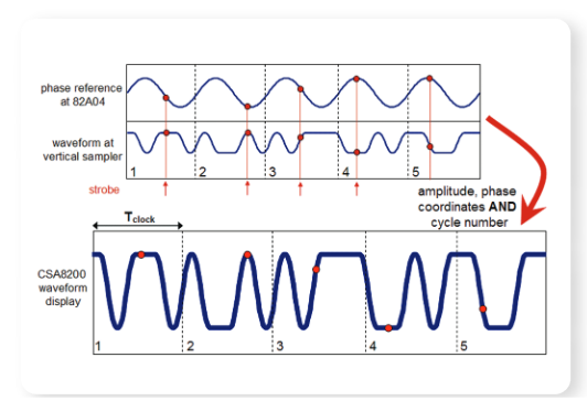
In Triggered Phase-Reference mode the user supplies a traditional trigger signal to either the dir ect or pre-scale trigger inputs. The oscilloscope employs its standard equivalent-time operation to acquire samples relative to the trigger point. The instrument then precisely phase- corrects the samples according to the simultaneously acquired corresponding phases of the reference clock. That way, the trigger determines where in the data stream the waveform record is taken.
An intuitive way of visualizing this concept is to think of the oscilloscope as counting the integer number of refer- ence clock cycles from the trigger point, then measuring the phase within the particular clock cycle where the sample is taken. The clock cycle number then provides an absolute reference with respect to the trigger point as illustrated in Figure 2. In this manner the horizontal axis is built up of consecutive r eference clock periods but the timing remains coherent to the trigger. The result is similar to the traditional sampling operating mode, but with substantially lower system jitter owing to the additional clock phase information.
Sampling oscilloscopes operating in standard, non-phase- corrected timebase mode usually contain small amounts of horizontal timing non-linearities. For applications that require the acquisition of wavefor ms with long record length it is crucial to have the highest degree of long-range time- base precision and linearity. The 82A04 combined with the Triggered Phase-Correction mode is a powerful tool to remove all sources of standard timebase inaccuracies from the system when a clean, stable reference clock is used, and yields the most precise, long-range timebase with unrivaled linearity.
Other instruments on the market do not support a triggered phase-correction mode and they are limited to the free- run mode. The triggered mode is the only way to view a complete single-valued pattern waveform with <200fs jitter edges instead of just an overlaid eye-pattern.
ITU-T recently created draft document O.172 which recommends a universal phase-analysis testing technique to accurately measure jitter after finding that commercial jitter analyzers showed wide discrepancies in reported jitter measurements on identical signals. ITU recognized the need to avoid the different measurement methods of these instruments. Instead O.172 specifies the use of a sampling oscilloscope in combination with a low-phase- noise synthesizer as a reference clock source. Pattern- dependent jitter is then determined by measuring the phase differences between the rising and falling edges of the data signal and that of the simultaneously acquired reference clock signal using the standar d timebase operation. Note that the essential elements of the ITU recommended method is inherently provided by the Triggered Phase-Reference mode of the CSA8200+82A04 in a convenient and highly accurate fashion.
The triggered phase reference mode enables the highest degree of accuracy in jitter and noise separation for advanced waveform and jitter analysis. Triggered phase- corrected mode returns the full functionality of an equiva- lent-time sampling oscilloscope to the user. This mode allows the traditional use of the oscilloscope to view long records with the same low &lp;200fs RMS jitter as the free-run phase reference mode. A user supplied pattern trigger, along with a reference clock, allow the user to view ultra-low jitter, entire-pattern waveforms. This triggered mode is not cur rently offered by any other low-jitter solution on the market.
Jitter Separation in Triggered Phase-Ref Mode
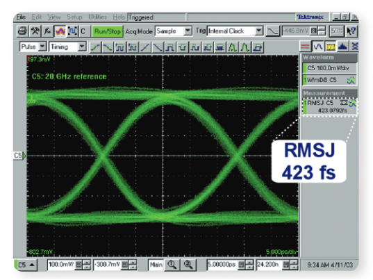
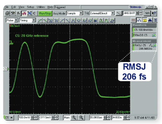
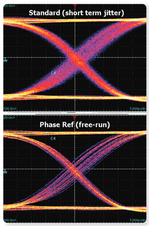
Figure 3 and Figure 4 show the same 40 Gb/s signal acquired in Free-run and Triggered Phase-Ref mode respectively. The eye diagram obtained in Free-run mode exhibits low jitter (423fs RMS ) but the edges obviously contain multiple components of jitter (ISI, data-dependent,residual random jitter leftover in Phase Refer ence module, un-correlated periodic jitter etc). The new Triggered Phase-Ref mode allows to "unwrap" the eye diagram as shown in Figure 4 if the applied trigger is synchronous with the repeating pattern length.
One can now measure the jitter on a single isolated edge (206fsRMS ) which contains only random system jitter and any uncorrelated jitter (periodic, crosstalk, etc). It follows that the difference of the two measurements is due to ISI and deterministic jitter.
When measuring jitter values, keep in mind that random Gaussian jitter is unbounded, and theoretically the measured peak-peak value can grow indefinitely with time. As a rule of thumb, acquisitions of signals with a few seconds of persistence (a few hundred waveforms) will experience a peak-peak jitter value that is nominally about 6 to 8 times the RMS jitter value.
Free-Run (untriggered) Mode
In free-run mode, the oscilloscope samples the vertical channel and corresponding reference clock phases randomly. Since different clock periods are indistinguish- able, the unique phase information is limited to one clock period, resulting in an overlaid display of all 0 to 2 π clock periods as illustrated in Figure 5. Note that in this mode, a trigger input is not required since the oscilloscope does not use the internal timebase hardware to sweep out the acquisition interval, and consequently the oscillo- scope can produce waveforms for any reference clock frequency that the 82A04 suppor ts. Thus, random sampling allows for trigger-free data acquisition. In a sense the reference clock forms a virtual trigger signal with a usable trigger bandwidth given by the bandwidth of the clock sampler. While the oscilloscope allows the user to adjust the horizontal range to display more than one clock period, it is important to keep in mind that any portions of the displayed waveform exceeding one clock period are simply filled with identical copies of the cor responding portions from inside the unique clock period. In other words, the on-screen waveform simply repeats after every clock cycle.
Unless the data pattern applied has a repetition rate that is equal to or shorter than the reference clock period, the waveform display generally results in eye patterns. Consequently, Free-run (untriggered) mode is most prevalently used with eye diagram analysis. It offers high timing accuracy but is highly constrained in its functionality by the fact that all data points "collapse" into a single clock period window.
Even relatively slow data rates with much mor e total jitter than the standard CSA8200 timebase can benefit fr om Phase Reference acquisition. In the example given in Figure 6, the individual data-dependent (ISI) dispersion of the edge from various data sequences can be more clearly seen when the phase reference module is used.
The lowest horizontal scale selectable in phase reference mode is as small as 100fs/div allowing the user to examine fast edges with high resolution.
Reference Clock Requirements
Most clocks are not ideal sinusoids; they may contain higher harmonics, duty-cycle distortion, aberrations and ringing. Excessive clock shape distortions, for example, may cause ambiguity in the clock phase extraction method if uncorrected for. Quantitative simulations of the effect of harmonic distortion on a hypothetical, uncor rected design show that a reference clock signal at 10 GHz containing 20% second-harmonic amplitude content would result in non-uniform system jitter degradation along the timebase of up to 30fsRMS. Likewise, a 10 GHz reference clock with 20% third harmonic amplitude content would (in an uncorrected design) lead to a jitter degradation of up to 60fs RMS
Clock Signal Filtering
To accept non-sinusoidal clock signals without the above mentioned performance degradation, the clock signal needs to be conditioned, i.e. its harmonic content needs to be reduced. To achieve this, the 82A04 employs internal filtering based on programmable bandwidth tuning of the clock sampler. The frequency response of the sampler is tunable and is set automatically to an optimum value when the user enters the clock frequency. This scheme generally provides adequate filtering for clock signals from 8 to 60 GHz. Below 8 GHz, the internal filtering of the 82A04 is less efficient and non-sinusoidal clocks ranging from 2 GHz to 8 GHz require the addition of external filtering. There are three optional
Filter accessories offered with the 82A04 covering the clock ranges 2-4 GHz, 4-6 GHz, and 6-8+ GHz. If the oscillo- scope encounters a clock signal with excessive distor tions during clock characterization, it warns the user of a "clock shape problem," in which case an external filter should be used to remedy the distortions. It is not recommended to attach a filter directly to the 82A04 input with a rigid SMA barrel adapter due to the mechanical str ess such a long lever-arm setup would introduce, possibly causing damage to the high fidelity, critically aligned 60 GHz input assembly of the 82A04. Instead, a flexible cable should be used between the 82A04 and the filter to allow for stressr eduction in the setup.
After filtering, the resulting clock shape in the 82A04 system will generally still have some r esidual non-sinusoidal content. As this error is slight, such imperfections can be character- ized and compensated by the clock calibration routine for the phase reference mode and will work adequately given that it remains stable.
In summary, it is desirable for good jitter performance to use clock waveforms with low harmonic content; above 8 GHz this is achieved with internal filtering. At lower clock frequencies an external filter might be needed. Here are additional key points to ensure maximum performance in Phase-Reference mode:
Intrinsic system jitter or, equivalently, horizontal timebase phase noise is determined by the random vertical noise of the clock voltage measurements. In order to achieve lowest instrument jitter floor, it is essential to maximize the signal-to-noise ratio of this clock measurement. The noise is comprised of two main components: the finite thermal noise of the sampling gate circuitry, and the amplitude noise contained in the reference clock signal itself. A perfectly noiseless clock ~1Vpp into the 82A04 will be limited by the internal sampler noise and residual jitter in the strobe delivery circuitry to ~150fsRMStimebase uncertainty. An effective way for the user to improve SNR is to increase the slew rate of the applied sinusoidal clock signal:
Use the highest reference clock frequency available for a given data rate. Note, however, that when in Free-Run mode this will reduce the period of unique data information.
Maximize the reference clock amplitude to utilize the entire dynamic range of 1.8 Vpp of the 82A04 input. The larger the clock signal, the less effect the fixed sampler noise has on measuring the clock signal voltages
It is recommended to use at least 600mVpp clock amplitude. While the module remains fully functional below 600mV pp the random noise contribution of the clock sampler becomes increasingly non-negligible relative to the lowered clock amplitude and will affect the phase uncertainty, thus leading to reduced instrument jitter performance.
Make sure that the 82A04 has been properly temperature compensated and its compensation status is within +/-5 Celsius of the last compensation (check under menu >Utilities>Compensation).
Measuring DUT Jitter Generation (Jitter Transfer Function)
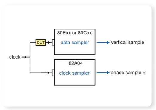
Figure 7 shows how to measure the jitter generation of a DUT. For most accurate results, it is necessary to measure the intrinsic contribution of the oscilloscope and the clock source to correct the total measurement and extract the contribution of the DUT. A clock signal is applied to both the phase reference module and to the vertical sampling module. Jitter measurements are repeated once with and once without the DUT in the vertical sample path. The setup without the DUT serves to establish the intrinsic jitter noise floor of the measurement system.
The jitter that is common is r emoved in a clock vs. data or in a clock vs. clock (including divided clock) signal that is applied to the Phase Reference system. Then the jitter generation that is produced with an added DUT inserted into the setup in the ver tical sample path can be compar ed against the setup lacking the DUT in the path and the jitter generation of the DUT can be measur ed.
Note that in most cases, the instrument and DUT jitter contributions are random and uncorrelated and therefore the rms jitter values add as the root sum of the squares of the individual contributors (assuming each has a Gaussian noise distribution).
An important point to mention is that in order to obtain the lowest possible jitter floor one has to keep the cable path from the clock source to the vertical sampler and to the phase reference module equidistant. This ensures that any phase noise contained in the clock synthesizer is synchronous at the sampling gates, i.e. the phase noise is sampled coherently and is thus removed from the measurement. On the other hand, if you are interested in looking at the phase noise of the clock source itself, an appropriate delay can be added in the non-DUT setup of Figure 2 in one of the cable paths. In this case clock phase noise is sampled incoherently (above frequencies corresponding to the differential propagation delay) resulting in increased jitter values compared to the setup using equal length cables. By using various delay lengths, you can, in principal, examine dif ferent phase noise frequency ranges.
Flexibility
The unique triggered Phase-Ref mode of the CSA8200/ 82A04 also enhances FrameScan ® to a new level of timing accuracy. Scanning a bit sequence at a very high accuracy can easily display sub-picosecond ISI problems, in particular with averaging turned on. The Phase-Ref module timebase is necessary for this.
If a reference clock is not available, the recovered clock output from a clock recovery module can be used. The TDS/CSA8200 family of plug-ins offer integrated optical, as well as dedicated electrical clock recovery modules for all standard rates from 50 Mb/s to 12.6 Gb/s; the acquisition jitter performance in this case tracks that of the clock recovery. The use of clock recovery in combina- tion with a low jitter phase-r eference timebase module in the same mainframe is possible because of the available 6 plug-in slots of the TDS/CSA8200 mainframe. Actually, a phase reference timebase, clock recovery and up to 4 data acquisition channels (either 4 electrical channels, or 2 optical and 2 electrical channels) can be used simulta- neously in a single mainframe. If clock recovery is not required then a total of up to 6 data acquisition channels can be configured in phase-reference timebase mode.
The Phase Reference module meets all of its specifications when operating on an electrical module extender cable. The use of an extender cable conveniently allows the movement of the phase reference module to a location where access to a clock signal or DUT is available (in cases where space or cabling limitations prevent the clock signal to be supplied to the mainframe's location).
Acquisition Speed
The phase re-ordering algorithm in phase reference mode is performed in real-time and is computation intensive. The CSA8200 employs dedicated DSP for each acquisition channel enabling it to acquire data at an unrivaled rate of up to 57 kSamples/s in Phase-Ref mode and is more than 50% faster than other solutions in ultra-low jitter mode. The high acquisition rate suppor ts the use of averaging in combination with Framescan to remove random vertical noise and gain fast insight into both vertical and horizontal deterministic components of the user signa
Conclusion
The architecture of the 82A04 allows for a more flexible and compact implementation of an ultra-low jitter time-base, and avoids the limitations of competing products which are based on fixed, bulky components and non-adjustable, discrete filters to implement clock filtering and phase sampling.
The 82A04 together with the CSA/TDS8200 implements the phase reference timebase functionality in a novel way, giving the user the freedom to select from time- base and acquisition modes without compromises. Any phase-reference frequency within the operating range is accommodated, and even advanced features, such as FrameScan ® , remain available. It is the only sampling oscilloscope on the market offering a continuous reference clock frequency range from 2 to 60 GHz, as well as the powerful Triggered Phase-Reference mode. The CSA/TDS8200 architecture, with separate DSP per acquisition slot, enables the acquisition rate in phase reference mode to reach over 57 kSamples/s, and is well suited for demanding laboratory research work, as well as for throughput-critical manufacturing environments.