Introduction
Threshold voltage (Vth) is a fundamental electrical parameter of MOSFETs (metal oxide semiconductor field effect transistors). The threshold voltage (Vth) is the minimum voltage applied to the gate to establish a conductive channel between the drain and source terminals of the MOSFET. There are several methods to determine the threshold voltage from the device’s transfer characteristics, the drain current (Id) vs. gate voltage (Vg) curve. When testing silicon carbide (SiC) MOSFETs, a forward gate voltage sweep followed by a reverse gate voltage sweep exhibits a hysteresis effect. This effect is primarily due to traps and causes a shift in the thresholdvoltage. This threshold voltage difference can affect some device parameters such as the leakage current and on- state resistance.
To eliminate or reduce threshold voltage hysteresis, JEDEC (Joint Electron Device Engineering Council) introduced the JEP183A standard to provide guidelines for measuring the threshold voltage of SiC MOSFET devices. This standard describes methods that use a conditioning pulse prior to generating the drain current vs. gate voltage sweep that is used to determine the threshold voltage.
Starting with the Clarius+ V1.14 Software Suite release, threshold voltage tests for SiC MOSFETs based on the JEP183A standard are included with the 4200A-SCS Parameter Analyzer. These tests, which utilize two source measure units (SMUs), are executed through the Clarius software interface.
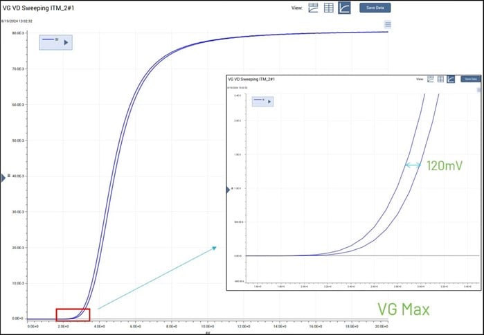
Figure 1. Exhibited hysteresis effect of Id vs. Vg curve of SiC MOSFET.
This application note discusses using the 4200A-SCS Parameter Analyzer to make accurate threshold voltage measurements on SiC MOSFETs based on the JEDEC JEP183A standard.
JEDEC JEP183A Standard
The JEDEC JEP183A standard, “Guidelines for Measuring the Threshold Voltage (Vt) of SiC MOSFETs”, addresses the hysteresis effect exhibited by traditional tests used on silicon MOSFETs. The hysteresis is caused by the increased number of traps in the SiC/SiO2 interface in SiC devices that causes a shift in the transfer curve between the forward and reverse sweeps.
The hysteresis can be observed by sweeping the gate voltage from 0 V to the maximum gate voltage and then back to 0 V. The SiC MOSFET drain current vs. gate voltage curve shown in Figure 1 demonstrates this effect. In this example, a difference of about 120 mV was observed between the forward and reverse curves. These sweeps were generated with the Clarius interactive software.
To address the hysteresis effect, a conditioning pulse is applied to the gate to help release the traps prior to a downward gate voltage sweep. The JEDEC JEP183A standard recommends that the conditioning pulse be set to the maximum gate voltage.
The JEP183A standard describes three different methods for threshold voltage measurements on SiC MOSFETs. All methods initially output a conditioning pulse on the gate but differ in how the gate and drain voltage are applied afterwards. These three recommended test methods are:
- Sweep Gate Voltage and Bias Drain Voltage Method
- Sweep Both Gate and Drain Voltage Method
- Bias Both Gate and Drain Voltage Method.
Details of these methods are further described in the JEP183A standard. The Clarius Library includes tests for performing the first two methods to extract threshold voltage. The following paragraphs explain how to use these Clarius Library tests.
Using the 4200A-SCS for SiC MOSFET Threshold Voltage Measurements
Setting up and executing the threshold voltage tests involves making connections to the device and using the Clarius software to configure and execute the tests.
Making Connections to the Device
Two SMUs and the ground unit (GNDU) are used for executing the threshold voltage tests as illustrated in the basic circuit diagram in Figure 2. Both SMUs are in the Force Voltage and Measure Current mode. The Force HI terminal of one SMU (SMU1) is connected to the gate terminal of the MOSFET and forces the gate voltage (Vg) including the conditioning pulse and a downward voltage sweep. A second SMU (SMU2) applies either a fixed or sweep drain voltage (Vd) and measures the drain current (Id). Force LO (GNDU) is connected to the source terminal of the MOSFET.
Not shown in the simplified circuit diagram are the SMU and GNDU Sense HI and LO terminals connected to the MOSFET. Using both the Force and Sense terminals enable a four- wire (or Kelvin) connection to the DUT to eliminate the lead resistance from affecting the measurement accuracy.
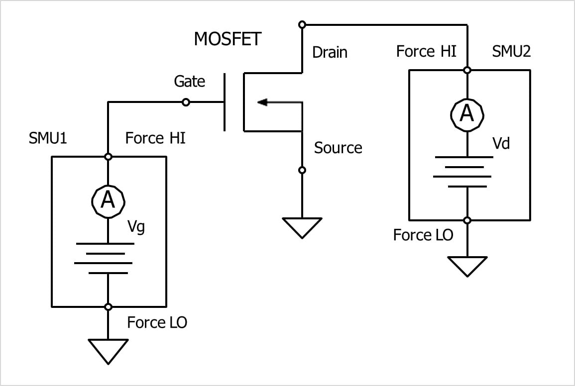
Figure 2. Simplified SMU connections to the gate and drain terminals of the power MOSFET.
Using the Clarius Software for SiC MOSFET Threshold Voltage Measurements
Tests for making SiC threshold voltage measurements are in both the Test and Project Libraries and can be found in the Select view of the Clarius interface by searching for the phrase “SiC MOSFET.” Once the tests are found in the Test Library, they can be selected and then added to a project tree. The Test Library includes tests (sic-mosfet-vth-vgsweep-vdfixed-smu and sic-mosfet-vth-vgvdsweep- smu) for both methods. As shown in the project tree in Figure 3, these two tests are also included in the project, sic-mosfet-threshold-voltage, which is in the Project Library. The tests are further described in the paragraphs to follow.
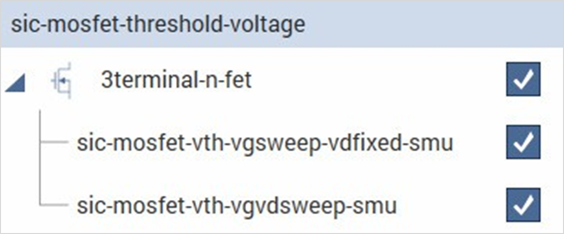
Figure 3. Project tree of sic-mosfet-threshold-voltage project.
Sweep Gate Voltage and Bias Drain Voltage Method
The first test, sic-mosfet-vth-vgsweep-vdfixed-smu, uses the Sweep Gate Voltage and Bias Drain Voltage Method that involves applying a conditioning pulse to the gate (Vg) using SMU1 and then downward sweeping the gate voltage (SMU1) while biasing a drain a voltage (SMU2). The drain current is measured by SMU2 and is plotted as a function of the gate voltage. The gate voltage (Vg), drain voltage (Vd), and drain current (Id) timing diagrams for this test are illustrated in Figure 4.
Also shown in the timing diagrams are the threshold voltage (Vth) on the Vg graph and the target drain current (Id Target) on the Id graph. From the user defined target drain current (Id Target), the threshold voltage (Vth) is calculated using linear interpolation.
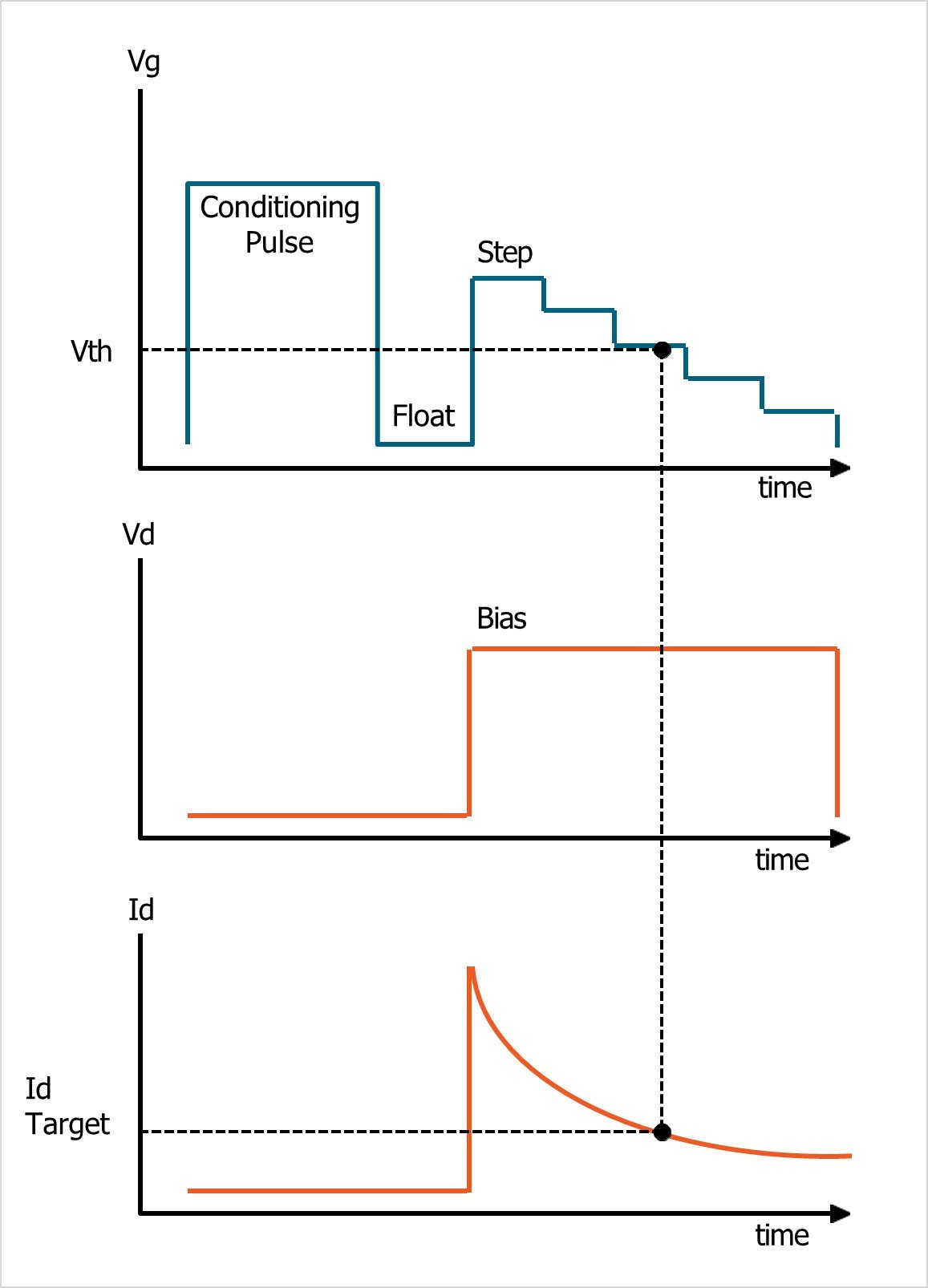
Figure 4. Gate voltage (Vg), drain voltage (Vd), and drain current (Id) timing diagrams of the sic-mosfet-vth-vgsweep-vdfixed-smu test.
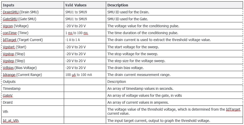
The input parameters of the test are set up in the Configure view of Clarius as shown in Figure 5. The test has settings for configuring the conditioning pulse, target drain current, drain current measure range, gate voltage sweep, and drain voltage bias. All the Input and Output parameters for this test are listed in the table in Appendix A.
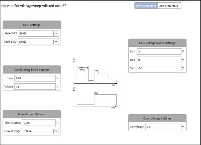
Figure 5. Configure view of the sic-mosfet-vth-vgsweep-vdfixed-smu test.
The JEDEC JEP183A standard recommends that the magnitude of the conditioning pulse be set to the maximum gate voltage. The step size of the voltage sweep should be kept small (0.1 V) to make an accurate threshold voltage calculation. The timing parameters in this test method require that the conditioning pulse be set between 1 to 100 ms and is user adjustable. The float time is the time between the end of the conditioning pulse and the beginning of the reverse sweep and is <10 ms and is not user settable. The time of each step in the reverse voltage sweep is also <10 ms and is not adjustable.
When the test is executed, the drain current is plotted as a function of gate voltage in the Analyze view graph as shown in Figure 6. The derived threshold voltage is represented as the red cross on the graph.
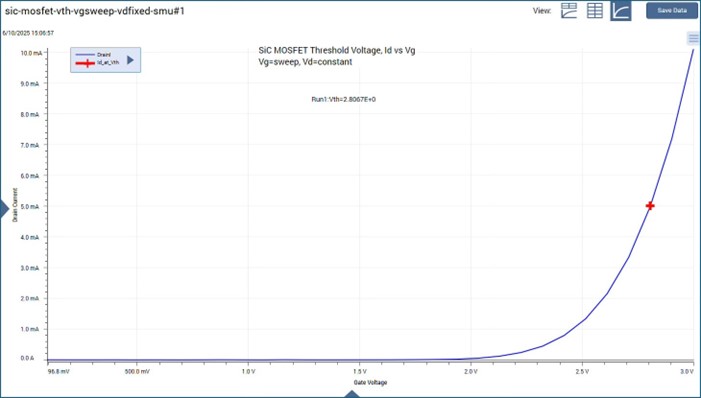
Figure 6. Id-Vg graph of sic-mosfet-vth-vgsweep-vdfixed-smu test showing Vth.
Figure 7 shows the screen capture from the Tektronix MSO5B Series Oscilloscope of the gate voltage (yellow) and drain voltage (blue) as output from the two SMUs.
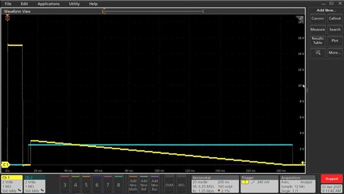
Figure 7. Oscilloscope Capture of sic-mosfet-vth-vgsweep-vdfixed-smu test.
All the measurements as well as the derived threshold voltage appear in the Sheet in the Analyze view. The first cell of the Sheet also shows any error codes from executing the code. All the error codes for both tests can be found in Appendix C.
This test was created using the SMU_vgsweepvdfixed user module in the wbg_ulib user library.
Sweeping both the Drain and Gate Voltage Method
The second test, sic-mosfet-vth-vgvdsweep-smu, applies a conditioning pulse to the gate (Vg) using SMU1 and then both SMUs output downward voltage sweeps of the same magnitude (Vg=Vd) to the drain (SMU2) and gate (SMU1) terminals. The gate voltage (Vg), drain voltage (Vd), and drain current (Id) timing diagrams for this test are illustrated in Figure 8. Like the previous test, the threshold voltage (Vth) is calculated using linear interpolation from the target drain current.
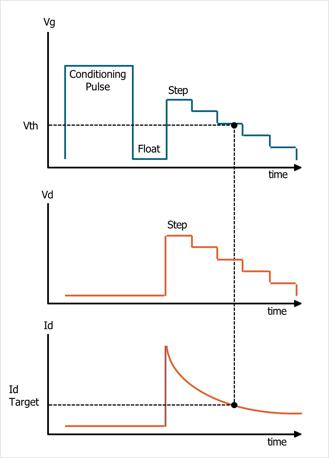
Figure 8. Gate voltage (Vg), drain voltage (Vd), and drain current (Id) timing diagrams of the sic-mosfet-vth-vgvdsweep-smu test.
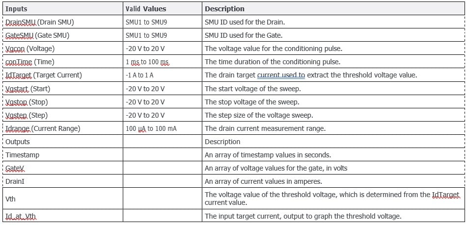
The input parameters for this test are set up in the Configure view as shown in Figure 9 and are similar to the ones in the first test but there is no drain voltage bias setting. The input and output parameters and their descriptions are listed in Appendix B.
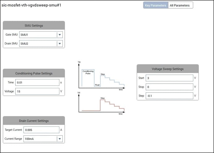
Figure 9. Configure view of the sic-mosfet-vth-vgvdsweep-smu test.
The results of executing this test are shown in Figure 10. Like the first test, the extrapolated threshold voltage appears as a red cross on the transfer curve.
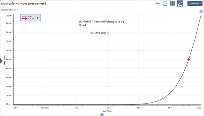
Figure 10. Id-Vg graph of sic-mosfet-vth-vgvdsweep-smu test showing Vth.
The oscilloscope waveform capture of the gate and drain voltages are shown in Figure 11. Notice the gate and drain voltage sweeps overlap since both sweeps are output simultaneously.
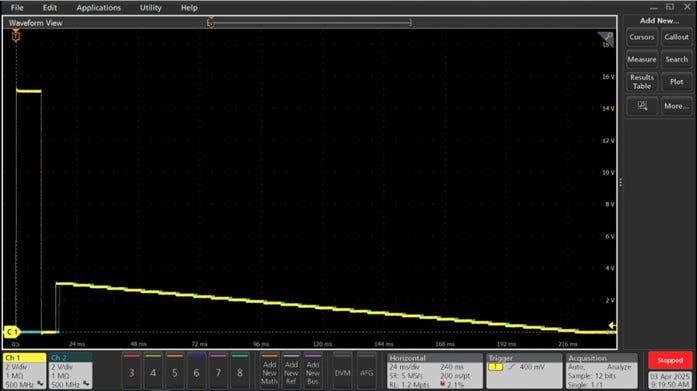
Figure 11. Oscilloscope capture of sic-mosfet-vth-vgvdsweep-smu test.
This test was created using the SMU_vgvdsweep user module in the wbg_ulib user library.
Conclusion
The 4200A-SCS Parameter Analyzer, paired with the Clarius+ Software Suite and two SMUs, enables accurate threshold voltage measurements on SiC MOSFETs using test methods based on the JEDEC JEP183A standard. These methods mitigate the hysteresis effect by applying a conditioning pulse to release traps. With its built-in test and project libraries, the Clarius software makes the 4200A-SCS a powerful tool for SiC device characterization.
Another SiC MOSFET test added with the Clarius V1.14 release enables quasistatic C-V measurements on SiC devices. Further details on this method are described in the Keithley application note, Forced Current Quasistatic C-V Method for SiC Devices.
Appendix A: Input/Output Parameters for sic-mosfet-vth-vgsweep- vdfixed-smu Test
Appendix B: Input/Output Parameters for sic-mosfet-vth- vgvdsweep-smu Test
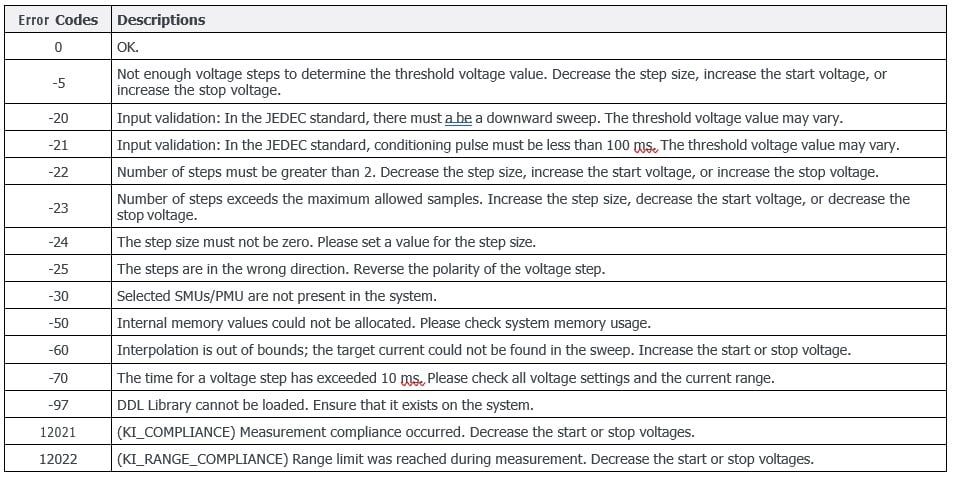
Appendix C: Error Code Descriptions