Introduction
Termed as the catalyst for the DTV revolution, High-Definition Multimedia Interface (HDMI) technology is on the threshold of mass adoption. Content providers, system operators and consumer electronics (CE) manufacturers are rallying behind this standard. As a result, the focus is now on demonstrating compliance to tests defined by HDMI standards. Design and validation engineers need tools to improve efficiency by performing a wide range of standards-required tests quickly and reliably.
This application note describes various tests that ensure validation, the challenges faced while testing complex HDMI signals and how oscilloscope-resident test software enables unprecedented efficiency improvements with reliable results and unprecedented automation to perform a wide range of tests (including the Sink tests).
Basics
HDMI leverages on the successful transition minimized differential signaling (TMDS) technology. The differential signals are +3.3 Volts, terminated in 50 Ω with nominal amplitude transitions of 500 mV (+2.8 V to +3.3 V). The voltage swing can vary from 150 mV to 800 mV. The signals have rise times of the order of 100 ps.
The data rates on a single link can range from 25 Mpps to 340 Mpps (Mpps = Mega pixel per second). Since each pixel is represented by 10 bits of data, the bit times, popularly referred as TBIT, can go down to 294 ps. A typical HDMI data signal is depicted in Figure 1. Most of the margins are defined with respect to TBIT – i.e. bit times for data signal.
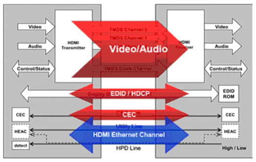
The TMDS transmission link comprises of three data channels and one clock channel. Figure 2 depicts the logical links of the TMDS signaling.
Physical Layer HDMI Compliance Standards
To ensure reliable information transmission and interoperability, industry standards specify requirements for the network's physical layer. The HDMI Specifications and, more specifically, the HDMI Compliance Test Specifications (or CTS) define an array of compliance tests for HDMI physical layer.
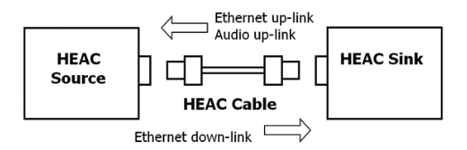
Figure 3 illustrates the major elements of the HDMI transmission system – source, cable and sink. The Source signals are characterized at TP1 while the sink devices are tested at TP2 to ensure that they are within standard margins. For testing cables, measurements need to be performed at both TP1 and TP2. Measuring at TP1 ensures measurements at TP2 are performed under known environments.
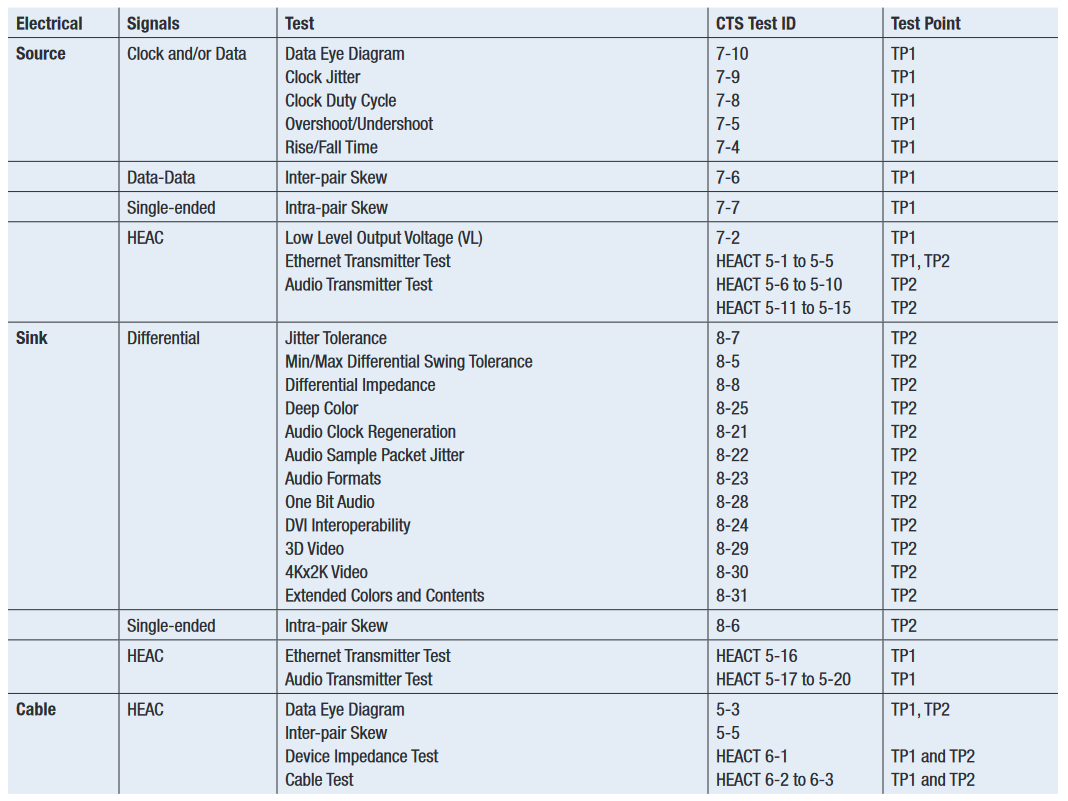
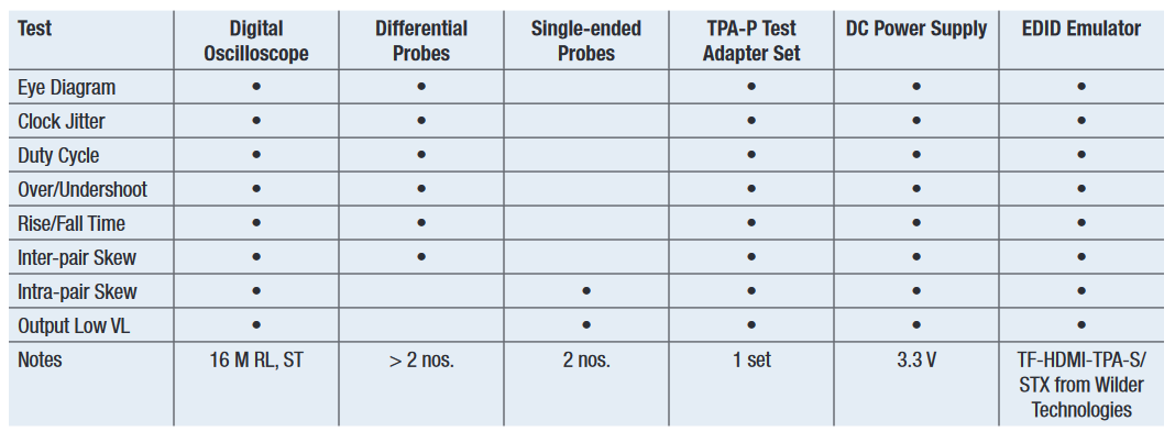
While it is recommended to perform as many tests as possible, the core tests are extremely critical for compliance.Table 1 summarizes some of the core tests:
Source Electrical Tests
These tests are performed on the clock and/or data signals at TP1. Considering the test setups, these can be further grouped as Clock-Data, Data-Data and Single-ended tests. The following sections will discuss these tests in more detail.
1. Clock-Data Tests
a. Data Eye Diagram Test
The objective of this test is to ensure the differential data has adequate "eye-opening" to enable effective recovery at the sink device after transmission. The data is clocked with respect to the recovered-clock and presented in a window size of +1.0 TBIT. Comparison to mask determines pass or fail and analysis of data jitter provides useful information on signal integrity.
The standard clearly delineates the method for clock recovery.The clock is recovered using a PLL function shown in Figure 4.
To ensure adequate representation of signal characteristics, the CTS specifies a minimum oscilloscope record length to acquire the data signal. This ensures that at least 400,000 unit intervals (or TBIT) are accumulated for building the eye diagram. With 16 M/20 M record length, at least 400,000 unit intervals can be captured for lower resolution signals, and over 2.6 M UI for higher resolution devices.
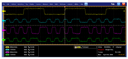
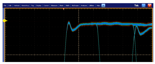
Figure 5 shows a screen-shot of eye diagram test being performed on the oscilloscope. The mask is shifted left until a violation occurs. Notice the tight margins, which imply strict discipline in violation detection. Typically, oscilloscope screens may have a pixel resolution of 500 x 400 or higher for the graticule and pass-fail testing is based on mask hits resolved by the screen image.
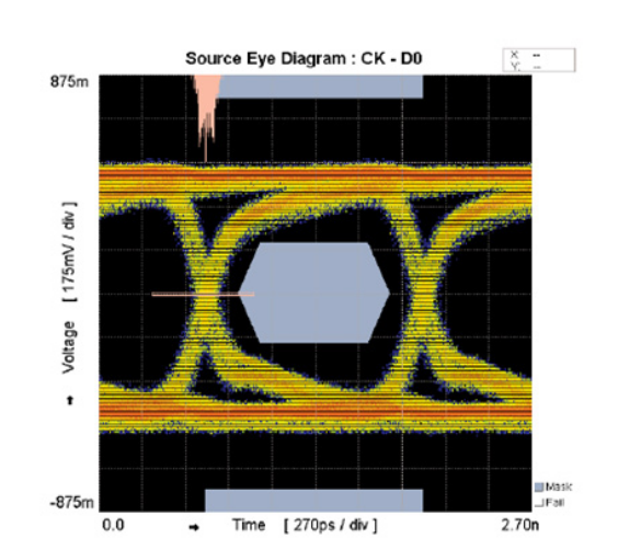
While this can be acceptable for lower HDMI resolutions, for higher speeds, results can often be misleading. In such cases it is preferable to perform mask violation testing down to data sample resolution. If this test were to be performed using image resolution, the results would have been incorrect.
b. Clock Jitter
At the nerve center of any transmission system is the clock signal. The jitter test checks to ensure that the clock signal is not carrying excessive jitter. In order to perform this test, the clock is referenced to a recovered clock. The standard defines the same clock recovery function as shown earlier in Figure 5.
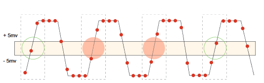
The clock signal is plotted with respect to the recovered clock. Histogram box is placed at the center of the edge and signal span determines the jitter present on the signal. The measured jitter should be less than 0.25*TBIT for compliance.
Traditionally, when measuring jitter using histogram box, the box is placed at the center of the rising edge and the height is kept at the minimum. This technique can be termed, for sake of convenience, as min-box approach.
It is important to recognize that at clock rates of the order of 340 MHz, number of samples on the edge might not be very high. In order to overcome the challenge of fewer samples, the size of histogram box could be increased vertically. In essence, it is no longer the min-box approach. This leads to higher jitter values as depicted in Figure 6.
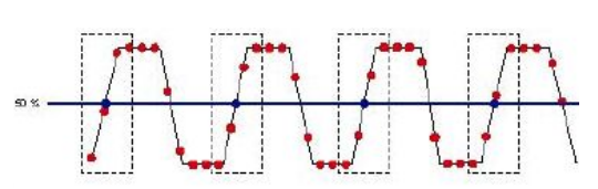
A better strategy is to interpolate samples and perform the measurement using the min-box technique. Figure 7 shows jitter measurement using interpolated samples using minbox approach. Comparing these values to those in Figure 6 demonstrates the effectiveness of interpolated min-box approach.
Another valuable jitter assessment technique is the Time Interval Error (TIE) method. In this case, the edge displacement is obtained for each cycle and the difference between minimum and maximum is presented as peak-to-peak jitter. Here again, interpolation lends higher resolution for precise analysis and testing.
c. Clock Duty Cycle
Duty cycle jitter is an excellent method of assessing deterministic jitter. The CTS defines the margin to be +10% from the nominal 50% duty cycle. Thus, the TDUTY measured should fall within 40% and 60%.
It is important that the variance in duty cycle is measured over large number of acquired signals. As per CTS, minimum 10,000-triggered waveforms are required for test purposes. Trigger re-arm rates of the oscilloscope take center-stage. Nominally, oscilloscope trigger re-arm rate are of the order of about 100 waveforms (wfms) per sec. This can mean unacceptably long acquisition and test times.
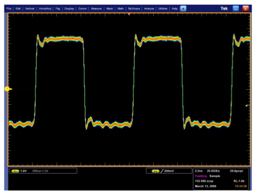
Fortunately, there are sophisticated techniques like FastAcq on Digital Phosphor Oscilloscopes (DPO) that enhance the trigger re-arm rates and deliver over 250,000 wfms/s. Figure 8 demonstrates the clock duty cycle test using the FastAcq™ technology. Notice the richness of information that ensures convincing measurements.
d. Overshoot and Undershoot
Overshoot and undershoot tests ensure that signals remain within prescribed limits. These tests ensure that the transmitter does not overdrive the channel or drive the ESD structures to become non-linear and start interfering. It also ensures interoperability by testing signals for recoverability.
The CTS standard defines the limit for overshoot as 15% and undershoot as 25% of the entire steady-state voltage swing. The test is performed on the clock as well as the data pairs. The test requires measurement of several parameters that includes accurate measurement of voltage swing (VH and VL) and overshoot and undershoots for both rising and falling edges. In all, this one test requires over six parameters before declaring results.
Besides the large number of parameters to be measured, it is also very important to ensure the measurements are performed authentically. It is important to maximize the size of the signal on the display in order to use as much A/D range as possible without overdriving. Figure 9 is a good example of accurate overshoot measurement technique. Tight margins require such careful measures for dependable results.
This test is not required to be performed as per CTS 1.4a. However, if the devices are tested as per CTS 1.2a, then this test is required.
e. Rise and Fall Time
Rise and fall time tests have been a mainstay in most physical layer tests. The limits ensure that signals deliver required signal speed and also that EMI is contained. The CTS specifies the rise or fall times should be higher than 75 ps and lower than 0.4 * TBIT value.
As in the case of clock duty cycle test, this test also requires large number of acquisitions. Once again, trigger re-arm rate becomes important. The test can be easily performed using FastAcq mode on a Digital Phosphor Oscilloscope.
The maximum rise and fall time is not required to be performed as per CTS 1.4a. However if the devices are tested as per CTS 1.2a then this is required.
f. Clock-Data Inter-pair Skew
Inter-pair skew is an extremely important test to ensure interoperability. This test confirms that skew between clock and any of the data pairs are within limits. The standard prescribes a limit on skew not to exceed 20% of the pixel-time (TPIXEL). This test is also performed between data channels as well. The next section on Data-Data tests describes this test in more detail.
This test is not required as per CTS 1.3c but is needed if tested as per CTS 1.2a.
2. Data-Data Tests (Inter-pair Skew)
The inter-pair skew test has several important aspects to be considered. Firstly, skew can be effectively measured only when both the pairs are transmitting a specific pattern. Secondly, the measurement paths (probes and oscilloscope acquisition system) could be introducing their own share of skew. Thirdly, the oscilloscope would need to trigger on specific serial patterns, also referred as serial triggering capability. Finally, the margins are specified with respect to the pixel time. Hence, it is important to also determine the clock rate accurately.
It is important to eliminate skew in the acquisition path. This process is termed as the “De-skew” process. For accurate results, it is better to perform de-skew prior to making this test.
3. Single-Ended Tests
These tests are performed on each pair using single-ended probes.
a. Intra-pair Skew
Intra-pair skew test gains significance, as the signals are differential and reveals several signaling artifacts. Skew within a differential pair is tested and the standards specify a limit of 15% of the bit time (TBIT). As in the case of Inter-pair skew, it is important to perform de-skew prior to performing this test. This ensures the error due to skew of the probing and acquisition system is minimized.
b. Low level Output Voltage (VL)
The VL test is performed to ensure signal voltage levels are within prescribed limits. The test checks for the DC voltage levels on the HDMI link for each TMDS signal. The CTS specifies that the voltage of the low-levels should fall within 2.7 V and 2.9 V.
In order to ensure compliance, large numbers of waveforms are analyzed. Standard prescribes a minimum of 10,000 waveforms. FastAcq helps perform this test faster. To determine the voltage level, histogram method is employed. The statistical maxima of the histogram (the histogram peak) is presented as the VL and compared against standard limits.
Preparing for Source Tests
a. The Test Suite
Table 2 summarizes the equipment required to perform the wide range of Physical Layer tests discussed earlier. Additionally, Digital Multimeter, Protocol Analyzer, LCR Meter and I2 C Analyzer are required to perform some of the other tests prescribed by the CTS standard.
b. Test Equipment - Important Considerations
While choosing the right equipment for your test setup, it is important to understand various aspects that need to be addressed. Some of these aspects are:
Digital Storage and Digital Phosphor Oscilloscopes
System performance drives measurement accuracy. It is important to consider the rise times of your HDMI signals while selecting the bandwidth required. A quick calculation on resolution supported, refresh rate and blanking period would provide a good indicator of the TBIT values. The TBIT values can be used to approximate the rise time of the HDMI signal (~0.2 to 0.3*TBIT).
At 165 MHz clock rate, the rise times can be between 75 ps to 250 ps. Tektronix’ TDS7704B, for example, provides rise times of the order of 60 ps and can be effectively used for signals with rise times greater than 180 ps. DPO70804 provides a rise time of the order of 33 ps and can also be used effectively for HDMI testing.
The eye-diagram and clock jitter tests require a minimum of 16 Meg record length. The eye diagram test is performed using two channels (Data and Clock) and 16 M should be available for both channels.
Several tests require large numbers of acquisitions (over 10,000 waveforms) and it is imperative to have fast trigger re-arm rates to perform the tests faster. FastAcq™ technology is available on many Tektronix oscilloscopes to enable faster testing.
The Inter-pair Skew test requires trigger on a specified serial pattern.
Differential Probes
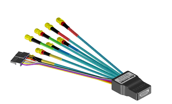
For example, two/four Tektronix P7313SMA probes could be connected using ET-HDMI-TPA-P adapter, which enables connections through SMA for reliable results. The HDMI TMDS signaling employs differential transmission system. Differential probes, with their high common-mode rejection, high sensitivity and response accuracy and low noise floor are well suited for this purpose. Considering the high signaling rates and tight margins, it is imperative to understand various aspects and options for probing. The primer – High-speed Differential Signaling and Measurements(3) provides in-depth understanding of these aspects.
Because differential probes have two identical input pins, making reliable connections is generally more challenging. It is important to carefully plan the connections to the test adapters with square-pins. Although there is a long list of probe tip adapters, each option must be weighed thoughtfully prior to employing any technique.
The Tektronix primer(3) dwells into finer details of each of these options. Variable spacing adapters, for instance, could result in excessive overshoot. Though inconvenient, soldering to the test points offers the best results. The P7380 and P7360 probe from Tektronix offers a variety of probe tips that allow soldering or holding the probe using a probe-positioner or a handheld probe housing to allow for point-to-point probing.
Probe bandwidth is another important factor to be considered. Again, depending on signal rise times, probes should be chosen to ensure its rise times are fast enough to ensure signal fidelity at the measuring instrument. Tektronix Oscilloscopes and Probes offer recommended system bandwidths right up to the probe tip.
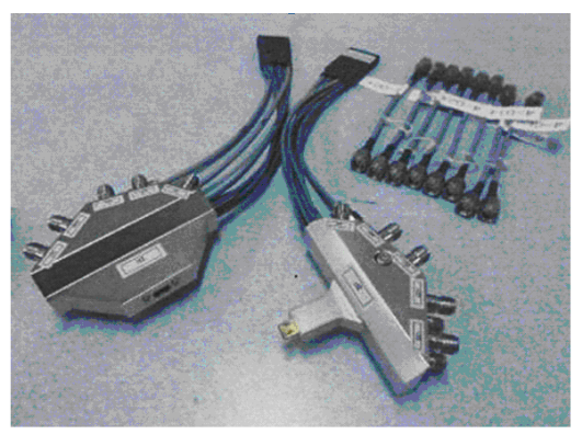
Test Adapter
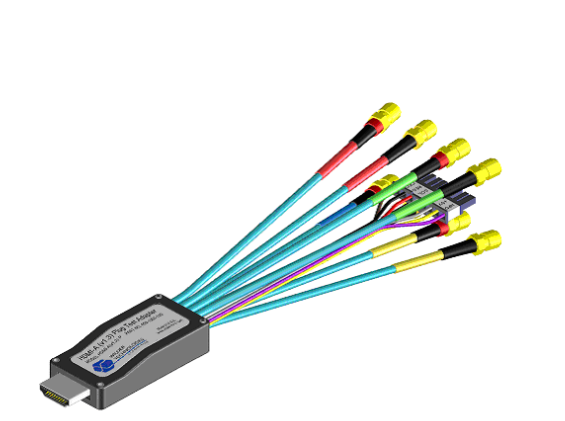
Reliable connections are key to maintaining precision and signal integrity. There are two types of test adapter sets available. For most of the Source devices, the plug-type adapters (TPA-P) are well suited for making the primary connection to the Device-under-test (DUT). Figure 10 shows a TPA-P plug-type test adapter from Wilder Technologies
Automation Tools
Compliance to Source tests implies performing a wide range of tests reliably. Tight margins and complex test procedures makes these tests very time-consuming. Most of the tests need to be performed under optimal conditions and users need to be an expert in HDMI technology as well as usage of test equipment. By any measure, a daunting task.
TDSHT3 discussed later in this document enables quick and reliable tests. Authentic measurement techniques ensure results that are reliable and automation relieves users of laborious and tedious test processes.
c. Test Setup for Source Tests
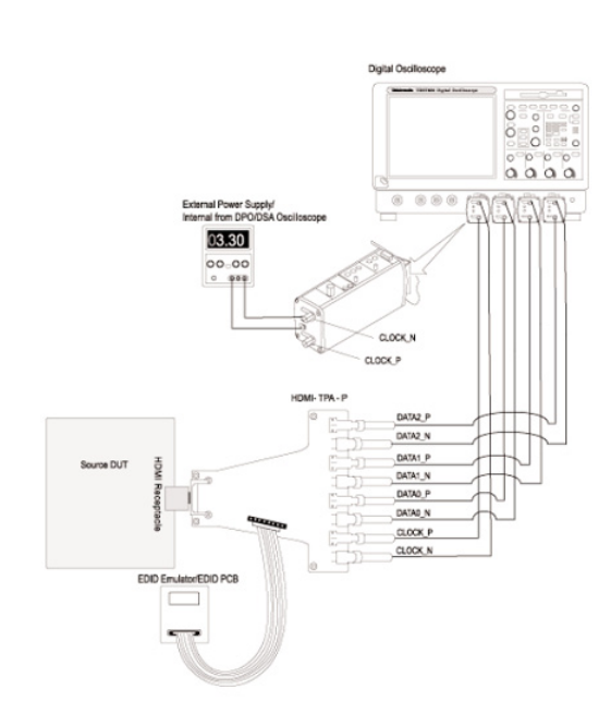
See Figure 11 for Differential Tests.
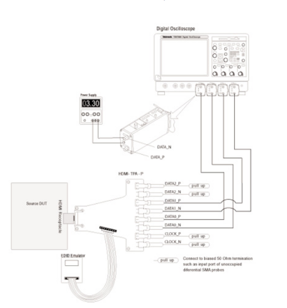
See Figure 12 for Single-ended Tests.
d. Getting the test signals from DUT
- Configure the EDID Emulator: This emulates a Sink device to enable handshaking of signals. Using a PC-based software, set the EDID Emulator to the desired resolution settings. One can use the Efficere EDID PCB. 8 Figure 10.
- Provide external power supply: Enables voltage across pullup resistors.
- There are no specified test patterns required and hence, any HDMI patterns generated by the Source DUT is adequate. For example, any DVD played on a DVD-player would generate required test signals.
Refer to the test setups described above for connection details.
Sink Electrical Tests
These tests are performed at the HDMI connector at the Sink Device at TP2. The following sections will discuss these tests in more detail.
1a. Jitter Tolerance Tests
One of the most critical characteristics of a sink device is its tolerance to specified levels of jitter in the signals. The standard defines the limit as 0.3*TBIT.
Specified amounts of jitter are injected in steps (from low to high jitter) into the transmitted TMDS signal until the sink device fails to recover the signal. The amount of jitter, which the sink device is able to tolerate, is compared against limits for compliance.
The jitter tolerance testing is performed in the following broad steps:
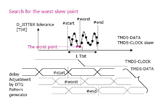
- Determining worst-case Clock-Data skew: The skew in data is varied until the worst point is determined. This test is performed over several iterations as described in Figure 13. The TMDS signal generator is then set to generate this worst-case skew.
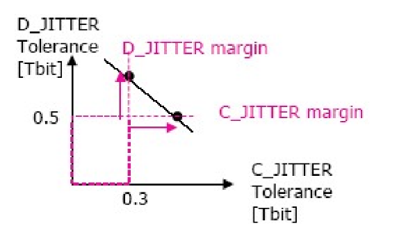
- Measuring Jitter Margins: Several measurements are carried out by injecting specified amount of jitter. Three measurements are performed over two test cases — (a) Data Jitter Frequency at 500 KHz and Clock Jitter Frequency at 10 MHz and (b) Data Jitter Frequency at 1 MHz and Clock Jitter Frequency at 7 MHz. The three measurements are:
- Data Jitter amplitude (Djw)
- Worst Data Jitter Amplitude (D_JITTER margin)
- Worst Clock Jitter Amplitude (C_JITTER margin)
Figure 14 helps understand measurement criteria for D_JITTER and C_JITTER margins.
With various parameters to be adjusted, and tight margins, this test tends to be extremely complex and takes a very long time.
1b. Jitter Tolerance Test
The Jitter Tolerance test in CTS 1. has been simplified to a great extent when compared to the test as per CTS 1.2a. The test is performed with all the jitter profiles (500 KHz, 10 MHz; 1 MHz, 7 MHz) and at 27 MHz, 74.25 MHz, 148.5 MHz, 222.25 MHz and if available at 297 MHz resolutions.
The jitter tolerance test in CTS 1.3c is performed in the following steps.
- Step 1: Create the worst case TP1 eye diagram by injecting 0.25 TBit clock jitter and 0.3 Tbit data jitter which results in a just pass TP1 eye diagram.
- Step 2 : Insert the first cable emulator (which emulates a worst case eye) for the resolution under test.
- Step 3: Adjust the clock jitter so as to measure a 0.3 TBit clock jitter at TP2 eye diagram.
- Step 4: Increase the skew between the lanes from 0 Tbit to 1 tbit in 0.1 tbit steps to observe failure of the Sink device.
- Step 5: Repeat steps 2,3 and 4 with the second cable emulator and find out if the Sink device fails.
HT3 software version 4.0.0 or above version now has limited margin test capability for Sink Jitter Tolerance test. Users can now insert jitter up to 0.5TBit.
2. Min/Max Differential Swing Tolerance
This test has been very common for most serial standards. The test confirms that the Sink properly supports interoperability even when the differential voltage swings are at their minimum levels (150 mV).
A TMDS signal generator with the ability to change amplitude is employed for this test. Any Sink-supported 27 MHz video format is generated that repeats the RGB gray ramp signals from 0 to 255 during each video period.
The testing starts from 170 mV VDIFF on all pairs and the differential swing is reduced in steps of 20 mV until the Sink device reports error. If the minimum VDIFF to which the Sink responds without error is < 150 mV, the device has passed the test. The test stops when minimum VDIFF reaches 70 mV.
Another important element of this test is that it is performed at two different VICM (common-mode voltage) settings, which are 3.0 V and 3.3 V. The CTS 1.3c asks for the signal to be also tested with a differential swing of 1.2 V.
3. Intra-pair Skew
The Sink devices also need to be tolerant to intra-pair skew. This test ensures the Sink device allows for timing skew within each TMDS pair. The CTS standard defines a limit of 0.4*TBIT for intra-pair skew tolerance.
The test starts by setting clock and data pairs with no skew and then increasing the intra-pair skew in each pair (one pair at a time) in steps of 0.1*TBIT until the Sink device outputs an error. The maximum skew with error-free Sink operation is defined as the Intra-pair skew and is compared against the limit. If greater than 0.4*TBIT, the device is termed compliant. TDSHT3 now supports 4-channel Intra-pair Skew test.
4. Differential Impedance
Differential transmission lines used in achieving fast data rates are very sensitive to impedance matching. Consequently, impedance characterization is a very crucial test in compliance testing of HDMI. The through-connection impedance has a limit of 15% variance to its 100 Ω specification. The impedance at termination needs to be tighter as the margins are only 10% of its characteristic value of 100 Ω.
This test is performed with the Sink device switched off. The measurement distance to DUT input connector is first measured. This is best determined using a TDR method where the impedance curve rises sharply to >200 ‰ denoting the distance to the connector.
Next, differential impedance values, ZDIFF, are determined for each pair from the input connector until the point where the impedance curve stabilizes to termination impedance. The other non-tested pairs are terminated to 50 Ω. ZDIFF values should fall within 85 Ω to 115 Ω for a device to pass the test.
To obtain a deeper understanding of TDR tests and measurement of controlled impedance, Tektronix offers some very descriptive application notes (4) and (5).
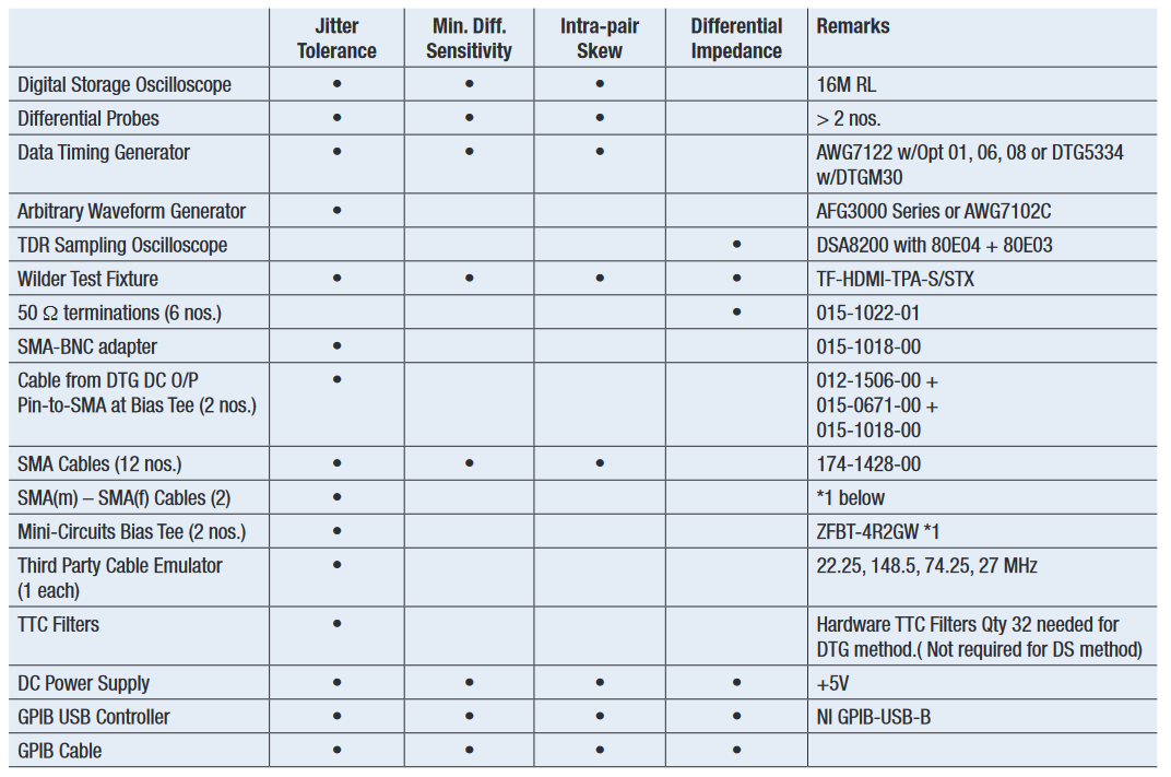
Preparing for Sink Tests
a. The Test Suite
Table 3 summarizes the equipment required to perform the Sink tests discussed earlier.
Additionally, Digital Multimeter, Protocol Analyzer and LCR Meter are required to perform some of the other tests prescribed by the CTS standard.
b. Test Equipments - Important Considerations
While choosing the right equipment for your test setup, it is important to understand important aspects that need to be addressed by this equipment. Some of these aspects are:
Digital Storage Oscilloscope
The jitter tolerance tests require a minimum of 16 Meg record length in the oscilloscope.
Data Timing Generator
TMDS Signal Generator plays a pivotal role in the Sink tests. The key challenge for a TMDS signal generator is to provide a full complement of highly accurate signals and the ability to precisely control their parameters.
For performing minimum differential sensitivity tests, a resolution of 20 mV is required. The intra-pair skew test requires precise delay settings down to sub-picosecond resolution. Tektronix offers the DTG5334 (with DTGM30 modules) that combines the power of a data generator with the capabilities of a pulse generator to enable the Sink tests with highly accurate test signals.
Arbitrary Waveform Generator
The jitter tolerance test assumes larger challenges as, both, clock and data jitter need to be varied. Generating jitter frequencies of the order of 10 MHz requires a combination of signal generators. Since margins are tight, precise control is required on jitter amplitude. Tektronix’ AWG7102 or AFG3000 is the platform of choice for generating such levels of performance.
TDR Sampling Oscilloscope
Time Domain Reflectometry (TDR) is a powerful and accurate tool for measuring impedance and length in interconnects. While fundamental concepts of TDR are relatively simple, a number of issues must be considered to make accurate measurements, the foremost being the ability to perform truedifferential TDR. This is what makes the DSA8200 with the 80E04 module the tool of choice for making the Differential Impedance test. If the TDR connection is to be probed to the circuit board, the 80A02 module can be combined with P8018.
If testing cables (such as in manufacturing), then the P8018 is not needed and just the the 80A02 with foot pedal actuator.This protects from possible operator error in connecting cables.
Test Adapter
Just as in Source tests, reliable connections are key to maintaining precision and signal integrity for Sink tests. There are two types of test adapter sets available. For most of the Sink tests devices, the plug-type adapters (ET-HDMITPA- P) set and receptacle-type adapters (ET-HDMI-TPA-R) set are well suited for making the primary connection to the Deviceunder-test (DUT). Figure 15 shows an ET-HDMITPA- R plugtype test adapter.
c. Test Setup for Sink
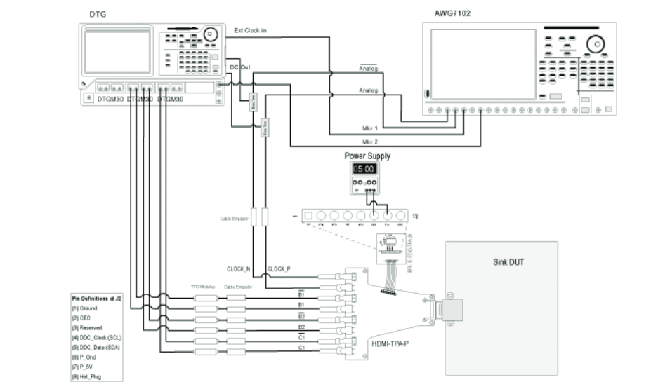
Tests Jitter Tolerance Tests (See Figure 16)
Minimum Differential Sensitivity (See Figure 17)
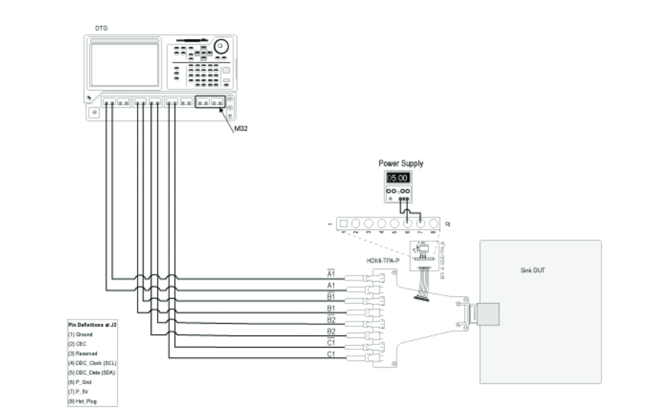
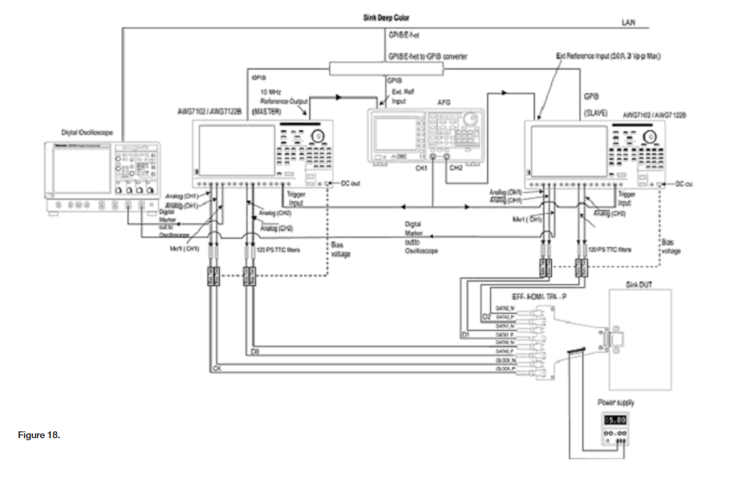
Intra-pair Skew tests (See Figure 18)
Automation Tools
Sink tests, as in case of Source tests, take a lot of time. In case of Sink tests, there is added complexity of controlling several tools to conclude a measurement. Add to that the challenge of precisely setting jitter parameters. All this makes automation an implicit requirement.
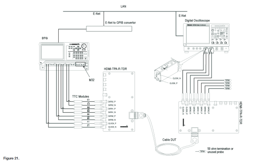
TDSHT3, discussed later in this document, de-skills the entire test process and makes use of GPIB to remotely control various parameters. The Digital Phosphor Oscilloscope connects to the DTG5334 using a GPIB cable and to the AWG using a GPIB-USB-B cable (available from National Instruments). The DPO/DSA70000 series oscilloscopes connects to the DTG5334 using GPIB cable and to the AWG using a GPIB-USB-B/HS cable or E-Net to GPIB converter (available from National Instruments).
Cable Electrical Tests
These tests are performed at the HDMI cable at both TP1 and TP2. The following sections will discuss these tests in more detail.
1. Data Eye Diagram Tests
The objective of this test is to ensure the cable relays the signal accurately from the Source to the Sink. The cable is expected to cause a certain amount of degradation to the signal. The test ensures the level of degradation is low enough to ensure interoperability between devices.
The signal is first characterized at TP1 prior to introducing the cable into the transmission system. An HDMI Signal Generator is used to generate TMDS signals. The HDMI Signal Generator parameters are adjusted to transmit signals carrying a specified amount of clock and data jitter. The eye-diagram and jitter tests ensure compliance to these test conditions and is performed similar to the Source tests.
The cable is then connected and the data eye diagram is verified again at TP2. The standard clearly delineates the amount of degradation permitted at TP2 by testing against several conditions:
- Mask tests
- Data Jitter is < 0.67 ns (equivalent to 0.5*TBIT at 75 MHz)
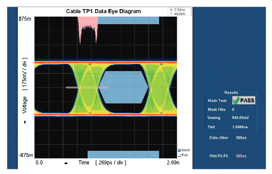
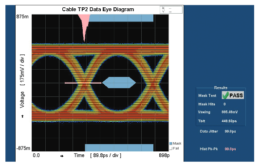
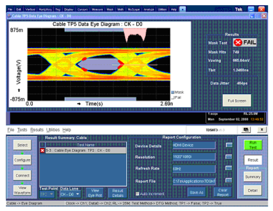
The data jitter is measured using a histogram box. Similar to Source jitter tests, min-box approach is highly recommended. The data jitter measured using min-box approach delivers reliable results. Figures 19 (TP1) and 20 (at TP2) illustrate a cable eye diagram test being performed on the oscilloscope.
2. Optional (Parametric) Tests
These tests are a very good indicator of the signal integrity of the cable. The tests are recommended, but not required.These tests are:
- Intra-pair Skew
- Inter-pair Skew
- Far-end Crosstalk
The Intra- and Inter-pair skew tests are performed using a sampling oscilloscope. The Tektronix TDS8200 used for Sink Differential Impedance test can be used for these tests using a TDT plug-in. The Tektronix 80E04 used for TDR can also be used for this test as it is a dual-channel sampler in addition to a dual-differential TDR step-generator. While the Far-end Crosstalk test is usually performed with a Network Analyzer, use of TDR for crosstalk measurements is gaining favor as the measurements can be performed faster, less expensively, and far more intuitively with TDR. TDA Systems has some informative application notes on measuring crosstalk with a TDR.
Preparing for Cable Tests
d. The Test Suite
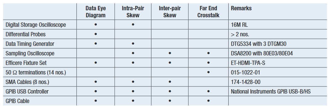
Table 4 summarizes the equipment required to perform the Sink tests discussed earlier.
A network analyzer can be used to perform the Far-end Crosstalk tests. Using a DSA8200 and I-Connect software you can now perform the tests which needed Vector Network Analyzers. This will provide a very good economical alternate test capability.
e. Test Equipment - Important Considerations
While choosing the right equipment for your test setup, it is important to understand important aspects that need to be addressed. Some of these aspects are:
Digital Phosphor Oscilloscope
The tests require a minimum of 16 M record length to ensure compliance to standards. Data jitter needs to be measured. It is also important to recognize that the jitter is measured with respect to the PLL-recovered-clock as described in the Source tests. As recommended earlier, min-box approach is most appropriate for reliable data jitter measurement.
Data Timing Generator
TMDS Signal Generator plays a pivotal role in the Cable tests. Tektronix offers the DTG5334 (with DTGM30 modules) that combines the power of a data generator with the capabilities of a pulse generator to enable the Cable tests with highly accurate test signals.
Sampling Oscilloscope
The limits for the skew tests require ultra-precision measurements. The DSA8200 with 80E04 or 80E03 modules deliver the required measurement accuracy and resolution for making these tests.
Automation Tools
Cable data eye diagram test brings the complexity of both Source as well as Sink tests. Complexity of eye-rendering, accurate data jitter measurement techniques coupled with the tedium of controlling several tools make this test very complex. TDSHT3, discussed later in this document, makes this test with relative ease. The Digital Phosphor Oscilloscope connects to the DTG5274 using a GPIB cable and to the AWG using a GPIB-USB-B/HS cable (available from National Instruments).
LiTek, from Taiwan offers a high-speed cable test solution (LT4165) that automates several other tests.
f. Test Setup for Cable Tests
See Figure 18 for Direct Synthesis setup for Cable tests.
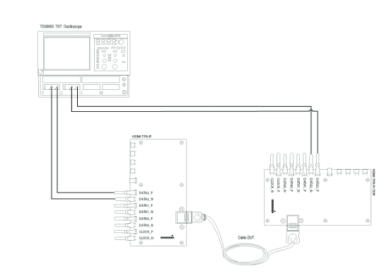
See Figure 21 for Data Eye Diagram Tests.
See Figure 22 for Intra-pair Skew Test.
See Figure 23 for Inter-pair Skew Test.
TDSHT3 HDMI 1.4a Compliance Software
Engineers designing or validating their HDMI physical layer need to perform thorough validation in-house. There are a wide number of tests that need to be made. These tests have tight margins requiring precise measurement techniques and complex control of a variety of test instruments. The standards also require many of the tests to be performed over various supported pixel resolutions, multiplying the complexity.
TDSHT3 HDMI Compliance Test Software automates a comprehensive range of tests, including Source, Sink and Cable tests, enabling unprecedented efficiency with reliable results.
Reliable and dependable results
TDSHT3 embeds the HDMI CTS 1.4a compliance test procedures, including the software clock recovery (SoftCRU), ensuring dependable results. Accurate eyerendering and precise violation testing deliver credible results. Sink tests are performed accurately with closedloop measurements that eliminate non-linearities of the test setup. Authentic measurement techniques and automation eliminate errors to provide convincing results.
Faster Validation Cycles
The unparalleled automation offered on the TDSHT3 enables faster validation. Test times for Sink devices shrink from hours to minutes with TDSHT3 remotely controlling the DTG and AWG to automate the complex test process. Its one-button "Select All" feature demonstrates efficiency by performing multiple Source tests. TDSHT3 instantaneously generates csvformat summaries or detailed reports at a press of a button.
Complete solution for validation
TDSHT3 offers a wide range of tests enabling thorough verification to standards. Tests offered include Source, Sink and Cable devices. With TDSHT3, convincing validation can be performed using a complete solution that includes oscilloscopes, arbitrary waveform generators, data timing generators, test fixtures and TDR.
Performing the tests using TDSHT3
User can select the entire range of tests by clicking on "Select All" button and run the tests at a press of a button. The Source tests are invoked when the Source tab is pressed.
The TDSHT3 Quick Start User Manual (6) provides examples of performing HDMI Source tests.
The user interface allows flexibility in setting up the tests and eliminates confusion.
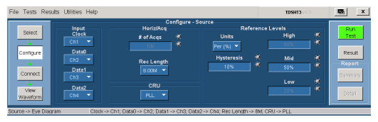
Source tests can be easily configured to various jitter parameters like amplitude and frequency while the software manages appropriate file transfer to DTG and AWG forb automated testing.
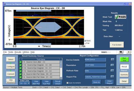
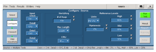
Pressing the Run Test button starts the test process and after performing all the tests, relevant plots are presented and result summary is provided as shown below.
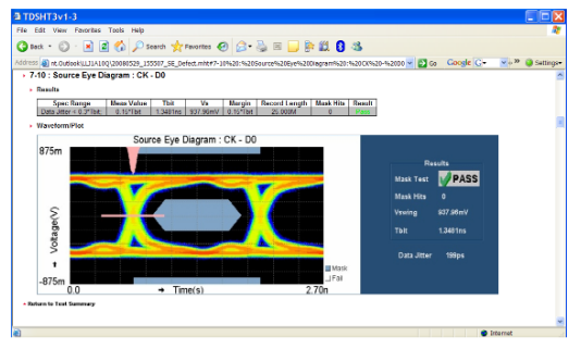
Pressing Result Details button provides more information on limits and measured values.
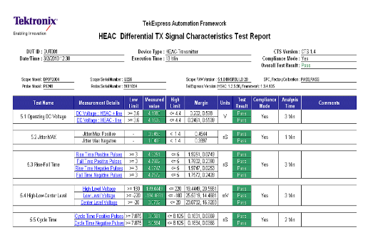
Report generation is instantaneous at the press of a button.The reports can then be easily converted in to popular formats such as portable document files and others.
The TDSHT3 Quick Start User Manual(6) provides examples of performing HDMI Sink tests.
A New Powerful Tool To Analyze ISI
Engineers Valuating High-speed Digital Serial Communication Who Need To:
- Isolate the particular bit sequences that cause mask violations.
- Remove noise and correlated Jitter on patterns as long as PRBS31-1 to evaluate deterministic effects such as Pattern Dependent Jitter and Inter Symbol Interference.
Specifications:
- Up to 6.25 GB/s NRZ or 8b/10b with internal clock recovery.
- Up to 2,147,483,647 bits pattern length.
Unfortunately the longest patterns, with the most stressful bit sequences including large numbers of Consecutive Identical Digits, place severe demands on test equipment. The problem is not only capture time but triggering capability.
Analysis methods that use data edges to trigger will ignore the Consecutive Identical Bits since there are no transitions. Pattern Lock triggers on recovered data clocks, not data transitions pattern lock, enables you to average and analyze serial data patterns up to 2.1 Gbs in length (PRBS31-1). By analyzing the digital data as a pattern you can isolate the particular bit sequences that are likely to cause mask violations.
Benefits
The TDSHT3 HDMI Compliance Test Software cuts validation cycles from days to hours. Authentic measurement techniques and closed loop measurements ensure reliable and dependable results. Its unparalleled automation shrinks test times and minimizes human-error. Coupled with a wide range of test equipment, it completes the solution for HDMI testing.
Reports can also be documented in comma-separated variable format by pressing the Summary button. This is very useful when testing multiple ports and documenting them as a summary. The csv format allows easy documentation in popular tools like Excel and many others.
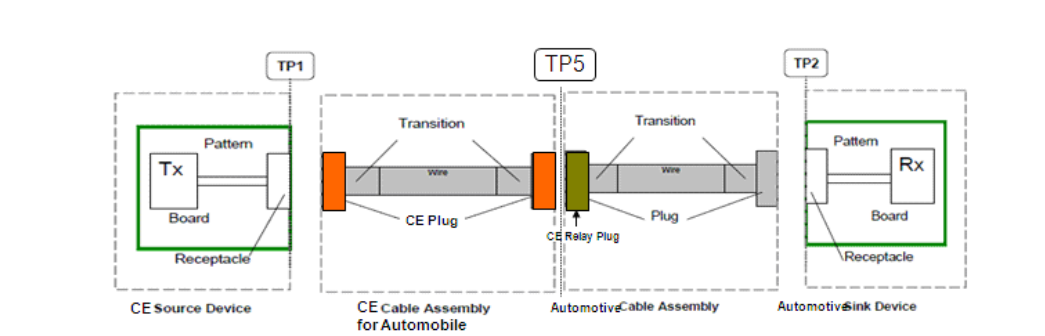
Automotive (Type E) and Mobile (Type D)
The Type 2 cable emulators have been approved in CTS 1.4a. The Direct Synthesis solution for Automotive HDMI has been approved in CTS1.4. DS solution for Type 1 and Type 3 CE has been approved in CTS1.4. Direct Synthesis solution supports all Cable emulators using the path breaking DS method which removes the need for hardware cable emulators thus enhancing the test method. Figure 24 shows the system components of the Automotive HDMI.
The HT3-DS software supports Automotive Type E HDMI testing as shown in Figure 25. The fixture for it is available from Tektronix and has been approved by the HDMI standards body.
Mobile companies will support the new Type D connectors as shown in Figure 27
HEAC
HPD/HEAC and reserved line forms full duplex balanced pair.HEAC consist of MLT3 signal in differential mode and IEC 60958-1 in common mode.
Source and Sink exchange 100BASE-TX data through a differential pair at the rate of 125 MSymbol/s (+/-100ppm) MLT-3 signal, which is simultaneously bidirectional (full-duplex).
The bidirectional signals do not necessarily have to be in synchronization with each other. The HDMI Sink device can transmits a single IEC 60958-1 stream as a common mode component of HEAC+/- differential pair signals to HDMI Source in reverse to the direction of the TMDS path with or without MLT-3 signals. This signal does not necessarily have to be synchronized with the MLT-3 signals.
HEAC lanes are biased to 4V through resistor from the Sink after detecting the HPD is active. HEAC allows the combination as signals are MLT-3 signal only, , IEC 60958 signal +MLT3 signal and IEC 60958 signal alone ) So there was no need of synchronizing MLT3 of TX and RX.
When an active Source and Sink are connected with a cable, the differential voltage across the termination resistance into one device is the sum of the driving signal of that device and signal from the other device. The device is able to detect with its sensor the MLT-3 signal and by subtracting the detected differential signal from its current driver's Signal. In addition, HDMI Source is able to detect with its sensor the IEC 60958- 1 signal by summing the differential signals, to extract the common mode signal.
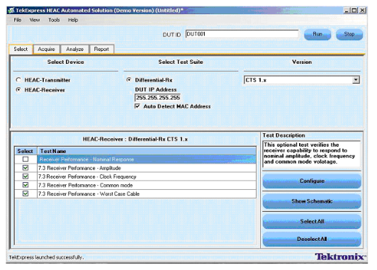
The following is a summary of the tests covered under HEAC Specification:
- Ethernet Transmitter Test
– Similar to normal 100Base-TX test except for lower amplitude - Ethernet Receiver Test
– Generate test packets with stress using AWG( 5K/7KB)
– Capture and analyze response packets using oscilloscope
– Confirm compliant packet error rate - Audio Transmitter Test
– SPDIF audio stream in common mode 400mVp-p amplitude
– 32k/44.1k/48k samples/s rate (up to 6.144Mbps)
– Measure typical pulse parameters using oscilloscope - Audio Receiver Test
– Generate test stream with stress using AWG
– Listening test to regenerated audible sound - Device Impedance Test
– Measure impedance of HEAC lines using TDR - Cable Test
– Measure impedance of HEAC lines using TDR/TDT
– Measure S-Parameters of HEAC lines using TDT+S/W
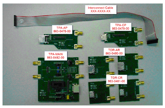
The HEAC Solution consists of the following:
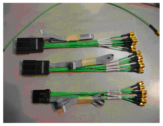
- Test Fixture Kit( TF-HEAC-TPA-KIT)
– One MAIN , 2 Plug ( AP/CP), 4#TDR ( 2#AR/2#CR),(Figure 30) - HEAC Software
– Ethernet Transmitter Test Software (Figure 28 and 29)
– Ethernet Receiver Test Software
– Control AWG & oscilloscope
– Setup signal (sensitivity, clock frequency, modal rejection, error rate)
– Extract & check response signal (software HYBRID & packet analysis)
– Audio Transmitter Test Software
– HEAC
– Audio Receiver Test Pattern Suite
– AWG files (format support, modal rejection, jitter tolerance)
Summary
High-Definition Multimedia Interface (HDMI) technology is witnessing rapid growth. As a result, the focus is now on demonstrating compliance to standards. Engineers designing or validating the HDMI physical layer on their products need to perform a wide range of tests, quickly, reliably and efficiently.
The large number of severe tests, coupled with unprecedented complexity, impose several challenges to the test engineer.Tight margins require careful measurements and thorough understanding of error contributors.
TDSHT3 enables efficiency improvements by performing a wide range of tests quickly and reliably.