Introduction
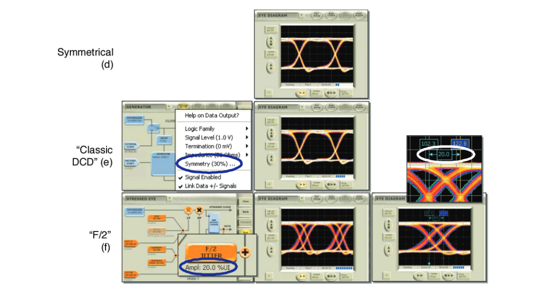
In most systems, it is desirable to have each data bit have the same duration (see Figures 1(a) and 2(d)). When bits vary in length, either randomly or systematically, this is known as jitter. One traditional form of systematic jitter is duty cycle distortion (DCD). For example, depending on bias setting, lasers transmitting NRZ (non-return to zero) data often have a delay before light is emitted, causing logic ones to be of shorter duration than logic zeroes. Frequently adjustments are made to the drive signal or bias settings of such a laser to eliminate the effect. An example is shown in Figure 1(b). All ones, wherever they occur in the data pattern, are shorter in this example than all zeroes. A commonly employed method of creating, or compensating for, this is to change the symmetry on a test equipment pattern generator (shown in Figure 2(e)). In the example eye diagram the pattern generator symmetry has been moved down 20% from the 50% symmetry point, and the crossing point on the eye diagram is visibly lower.
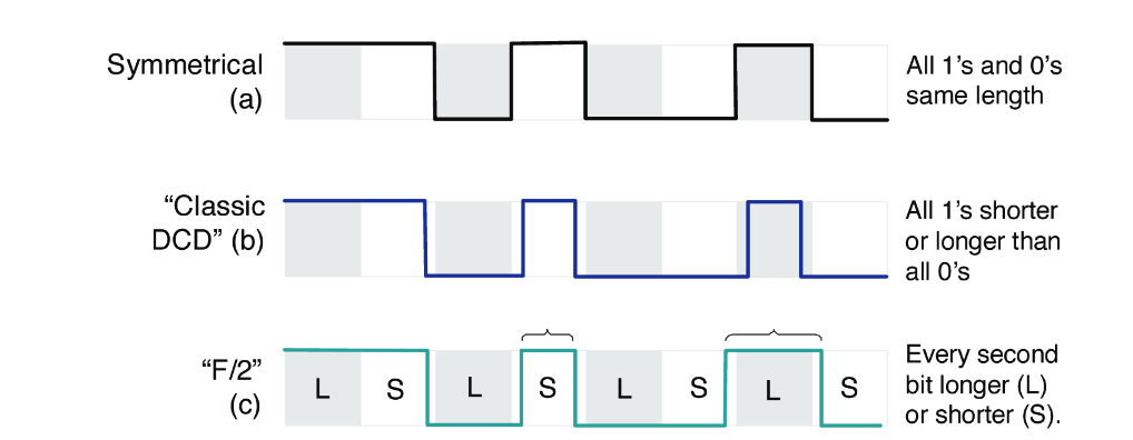
Recently it has become common for Gb/s systems, particularly those above 5 Gb/s, to employ architectures using a 2:1 mux in the final stage of their transmitters. Such multiplexers can be very sensitive to the duty cycle of the clock feeding them. The full rate clock is used to select between the two incoming half-rate data streams, with the high level selecting one, the low level the other. Any asymmetry in the clock will favor one incoming data stream over the other, resulting in longer bits from one side than the other. The outcome is that every second bit, independent of whether it is a zero or a one, will be longer or shorter. This is illustrated in Figure 1(c) with longer bits ("L") and shorter bits ("S"). As can be seen with the highlighted bits in Figure 1(c), ones (or zeroes) can be of different duration.
On a spectrum analyzer this kind of jitter is particularly obvious at half the data rate, and so is often known as "F/2" jitter, or shortened simply to "F2". An example is shown in Figure 2(f), generated with a BERTScope. Here, 20% amplitude F/2 was set in the stress setup, and the resulting eye diagram looks quite different to the 20% of classic DCD shown in Figure 2(e). The two distinct crossing points are shown to the right in Figure 2(f) measured with markers. The generator was set for 10 Gb/s to make the math easy, with 20 ps corresponding to 20%.
F/2 is a high frequency deterministic jitter component, and it is not easily compensatible in a system through the use of techniques such as receiver equalization. Because multiplexers can be prone to causing it in real systems, it is starting to appear in receiver jitter tolerance recipes, to ensure that receivers can cope well enough with it. An example is Backplane Etherneti (802.3ap, also known as 10GBASE-KR) where, although not explicitly stated, the introduction of 3.5% DCD is expected to be F/2. The current draftii of 8 GT/s PCI Express 3.0 shows F/2 jitter in the DCD eye diagram, and refers to it as "High Frequency AC Common Mode." F/2 is also a significant worry for standards groups working on USB 3.0, Fully Buffered DIMM, and QPI.