
A new generation of wide-bandgap (WBG) materials such as silicon carbide (SiC) and gallium nitride (GaN) are becoming more prevalent. Electrically, these substances are closer to insulators than silicon and other typical semiconductor materials. Their adoption is an effort to overcome limitations of silicon that stem from it being a narrow bandgap material, which leads to undesirable conductive leakages that become more pronounced with increases in temperature, voltage, or frequency. The logical extreme of such leakage is uncontrolled conductivity, which equates to failed operation as a semiconductor.
Of these two wide-bandgap materials, GaN is suited primarily to low- to mid-range power implementations, under approximately one kilovolt and 100 amps. A notable area of growth for GaN is its use in LED lighting, and usage is growing for additional low-power usages such automotive and RF communications. By contrast, the technologies surrounding SiC are both better developed than GaN and better suited to higher power implementations such as electric vehicle traction inverters, power transmission, large-scale HVAC equipment, and industrial systems.
Compared to Si MOSFETs, SiC devices are capable of operating at higher voltages, higher switching frequencies, and higher temperatures. Under these conditions, SiC provides higher performance, efficiency, power density, and reliability. This combination of benefits is helping designers reduce the size, weight, and cost of power converters, making them more competitive especially in lucrative market segments such as aerospace, military, and electric vehicles.
Because SiC MOSFETs enable higher energy efficiency from designs based on smaller components, they are instrumental in the development of next-generation power conversion equipment. At the same time, this transition also requires engineers to revisit some of the design and testing techniques that they have traditionally used when creating power electronics.
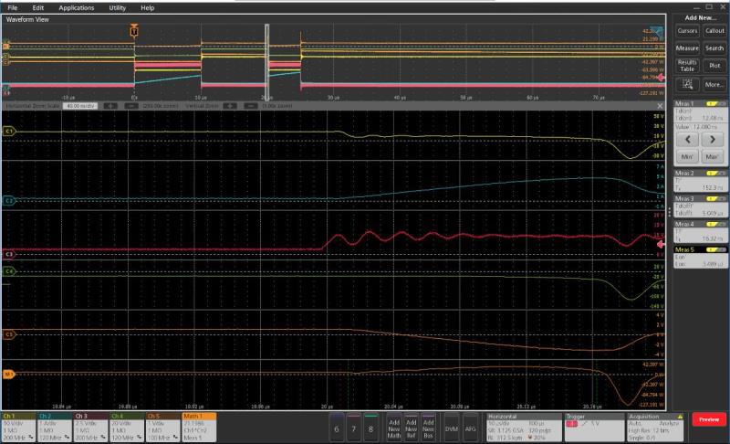
Double pulse testing software on a 5 Series MSO oscilloscope automatically measures energy loss during turn-on (Eon) and key timing parameters.
The Challenge… A Growing Requirement for Rigorous Testing.
In order to realize the full potential of SiC and GaN devices, accurate measurements during switching operations are needed to optimize efficiency and reliability. Testing procedures for SiC and GaN semiconductor devices must account for the higher operating frequencies and voltage levels of these devices.
Jonathan Tucker, Power Market Segment Leader for Tektronix/Keithley, recently authored an article in Electronic Design – Testing Requirements Evolve for Energy-Efficient Power Electronics. In it, he shared some thoughts on this new testing requirement:
"Advances in test and measurement tools such as arbitrary function generators (AFGs), oscilloscopes, source-measure-unit (SMU) instruments, and parametric analyzers are helping power design engineers obtain more robust results more quickly. This updated equipment helps them meet daily challenges.
Minimizing switch losses continues to be a major challenge for power-device engineers; these designs must be rigorously measured to ensure compliance. One key measurement technique is called the double pulse test (DPT), which is the standard method for measuring the switching parameters of MOSFETs or IGBT power devices."
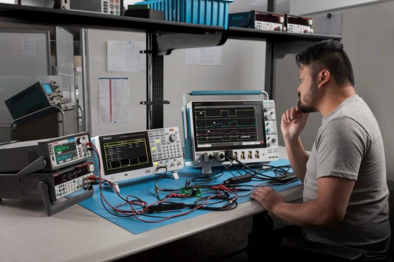
A setup for performing double pulse testing of SiC semiconductors includes a function generator for driving the gate of the MOSFET and an oscilloscope with analysis software for measuring VDS and ID.
In addition to double-pulse testing, a circuit-level test, there are material-level testing, component-level testing, and system-level testing that all need to be administered. Innovations in test tools enable design engineers at all phases of the life cycle to work toward power-conversion equipment that can cost-effectively meet rigorous design requirements.
Tektronix tools are positioned for WBG success.
Some of the tools from Tektronix that are positioned for today’s WBG requirements include:
- Source-measure-unit (SMU) instruments
- Arbitrary function generators (AFGs)
- Oscilloscopes
- Parameter Analyzer
Being prepared to certify devices against regulatory changes and the needs of new technologies from power generation to end user devices such as electric vehicles, enables companies that make power electronics to focus on the value-added innovation that defines the future.