
연락처
텍트로닉스 담당자와 실시간 상담 6:00am-4:30pm PST에 이용 가능
전화 문의
9:00am-6:00PM KST에 이용 가능
다운로드
매뉴얼, 데이터 시트, 소프트웨어 등을 다운로드할 수 있습니다.
피드백
전력 반도체 장치의 출시 기간 단축
전기 자동차 및 RF 통신의 까다로운 응용 분야에는 기존 실리콘의 지속적인 사용과 함께 SiC 및 GaN과 같은 와이드 밴드갭 반도체 기술이 필요합니다. SiC와 GaN은 Si에 비해 전압 작동 주파수와 온도, 전력 손실이 낮습니다. SiC와 GaN의 전기적 성능을 이해하면 새롭게 떠오르는 많은 전력 응용 분야에서의 활용 가능성에 대한 강력한 가치 제안이 가능합니다. 현장에서 장치 오류를 최소화하는 동시에 전력 반도체 장치의 출시 기간을 단축할 수 있습니다.
광대역 밴드갭 반도체를 위한 I-V 특성화 측정

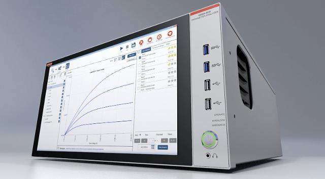
I-V 특성화
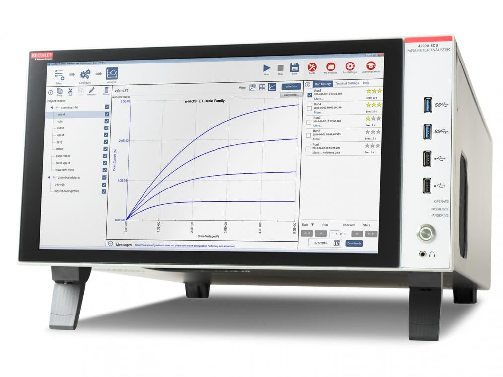
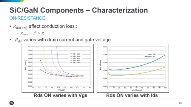
IV 특성화는 실리콘, 탄화규소 및 질화갈륨에서 기본 물성의 전류 대 전압 관계를 이해하는 기본적인 방법입니다. SMU 또는 매개 변수 분석기와 같은 장비와 적절한 소프트웨어를 사용하여 전자 장치 또는 회로를 통해 흐르는 전류와 해당 단자에 인가된 전압 간의 관계를 보여주는 데 사용되는 I-V 그래픽 곡선을 생성합니다. 가장 일반적인 I-V 곡선 세트는 곡선 집단입니다.
광범위한 전력 엔벨로프에서 테스트
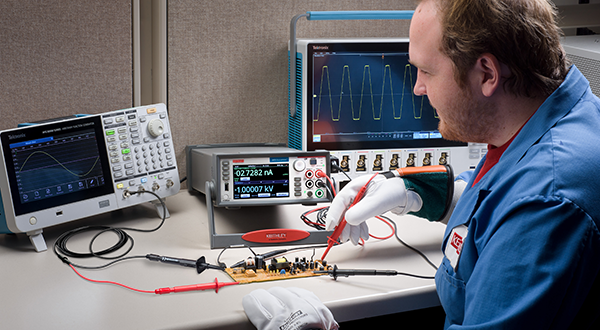
전기적 성능을 위해 SiC 또는 GaN 웨이퍼 및 패키지 부품 레벨 장치를 특성화하려면 고전력 장비 활용, 프로빙 문제 처리 및 낮은 레벨(예: 높은 브레이크다운 전압이 존재하는 곳의 피코암페어 레벨의 누설 전류) 측정 수행과 같은 새로운 기술을 학습해야 합니다. 광대역 밴드갭 반도체 경우, 최대 3000V의 전압과 최대 100A의 전류를 소싱하는 것이 더 일반적입니다. 마찬가지로 중요한 것은 ON 상태, OFF 상태 및 커패시턴스 측정을 위해 설정을 변경하는 데 걸리는 시간을 줄이기 위해 테스트 시스템을 최적화하는 것입니다.

전력 세미 장치의 브레이크다운 테스트
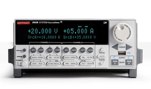
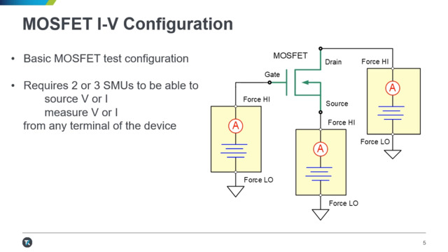
장치의 OFF 상태 브레이크다운 전압에 따라 장치에 인가할 수 있는 최대 전압이 결정됩니다. 전력 관리 제품 설계자가 관심을 갖는 주요 내전압은 MOSFET의 드레인과 소스 또는 IGBT의 집전 장치와 이미터 사이의 브레이크다운 전압입니다. MOSFET의 경우, n형 장치에 음전압을 인가하거나 p형 장치에 양전압을 인가하는 등 게이트를 단락시키거나 강제로 "하드" OFF 상태로 만들 수 있습니다. 이것은 하나 또는 두 개의 소스 측정 장치(SMU) 장비를 사용하여 수행할 수 있는 매우 간단한 테스트입니다.
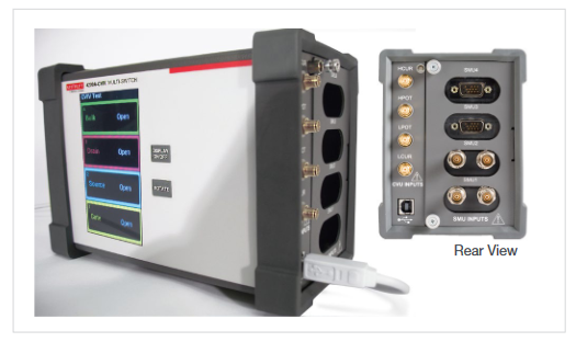
프로버 및 테스트 픽스처에 장비 연결
고전력 장비를 프로브 스테이션 및 테스트 픽스처에 연결하는 것은 복잡한 작업일 수 있습니다. 부적절한 연결은 종종 측정 오류로 이어질 수 있습니다. 8020 고전력 인터페이스 패널은 Keithley SMU와 다양한 반도체 프로브 스테이션 또는 맞춤형 테스트 픽스처 간에 매우 정확하고 유연하며 사용하기 쉬운 인터페이스를 제공합니다. 인터페이스 패널에는 3kV, 200V 및 100A 측정을 수용하는 6개의 측정 경로가 있습니다. 프로브 스테이션에 맞게 다양한 출력 커넥터 유형으로 5개의 경로를 구성할 수 있습니다. 선택적 바이어스 티로 4개의 경로를 구성할 수 있습니다. 이는 테스트 대상 장치의 최대 4개 핀에서 고전압 C-V 측정을 제공합니다.


8010 고전력 장치 테스트 픽스쳐는 최대 3kV 또는 100A의 고전력 장치를 테스트하기 위한 안전하고 간편한 연결을 지원합니다.
자세히 보기:
고전력 테스트 수행 시 안전 최우선
광대역 밴드갭 반도체에 대한 고전력 테스트를 수행할 때는 반드시 안전을 최우선으로 고려해야 합니다. 실험실을 위한 안전하고 규정을 준수하는 테스트 픽스처를 설계하는 것은 간단하지 않습니다. 8010 고전력 장치 테스트 픽스처는 최대 3000V 및 100A의 다양한 유형의 패키지 장치를 테스트할 수 있는 안전하고 노이즈가 적은 완벽한 환경을 제공합니다. 교체 가능한 소켓 모듈 테스트 보드는 사용자 제공 소켓 유형을 포함하여 다양한 패키지 유형을 허용합니다.
I-V 특성화를 위한 전력 시퀀싱 자동화
Keithley의 ACS(자동 특성화 제품군) 소프트웨어를 사용하면 테스트를 프로그래밍하는 수고를 덜 수 있습니다. ACS는 장치 특성화, 파라메트릭 테스트, 안정성 테스트, 단순 기능 테스트까지 수행할 수 있도록 설계된 유연한 대화형 소프트웨어 테스트 환경입니다. ACS는 다양한 Keithley 장비 및 시스템, 하드웨어 구성 및 테스트 설정을 지원합니다. ACS를 활용하면 자동화된 하드웨어 관리 툴을 사용해 장비를 구성하고 프로그래밍 지식이 없어도 빠르게 테스트를 수행할 수 있습니다.


-power-electronics-systems/fig-16.png?h=696&iar=0&w=1192)