Current Language
×
Korean (Korea)

언어 선택:

메뉴 전환
Current Language
×
Korean (Korea)

언어 선택:

연락처

텍트로닉스 담당자와 실시간 상담 6:00am-4:30pm PST에 이용 가능

전화

전화 문의

9:00am-6:00PM KST에 이용 가능

다운로드

매뉴얼, 데이터 시트, 소프트웨어 등을 다운로드할 수 있습니다.

다운로드 유형
모델 또는 키워드

피드백

4200A-SCS 파라미터 분석기를 사용한 MOSFET 게이트 전하 측정


소개

파워 MOSFET는 다양한 분야에서 사용되며 고속 스위칭으로 사용할 수 있습니다. 장치의 스위칭 속도는 내부 커패시턴스의 영향을 받으며, 보통 데이터 시트에 Ciss 및 Coss로 명시되어 있는데, 이는 입력 게이트와 드레인 커패시턴스인 Cgs 및 Cgd에서 도출된 것입니다. 게이트 전하(Qgs 및 Qgd)를 사용하면 커패시턴스의 명시 외에 MOSFET의 스위칭 성능도 평가할 수 있습니다.

MOSFET 게이트 전하의 게이트 전하를 측정하는 방법은 JEDEC JESD24-2 표준 "게이트 전하 테스트 방법"에 나와 있습니다. 이 방법에서는 게이트-소스 전압이 시간의 함수로 측정되는 동안 게이트 전류가 강제됩니다. 결과 게이트 전압 파형에서 게이트-소스 전하(Qgs), 게이트-드레인 전하(Qgd), 게이트 전하(Qg)가 도출됩니다.

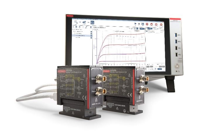
4200A-SCS 파라미터 분석기는 두 개의 소스 측정 장치(SMU)와 시스템에 포함된 게이트 전하 측정 테스트를 사용해 MOSFET 게이트 전하 측정의 수행을 지원합니다. 이 테스트는 4200A-SCS Clarius+ 소프트웨어 제품군에서 제공되는 광범위한 테스트 라이브러리에 포함된 여러 테스트 중 하나입니다. 이 애플리케이션 노트에서는 4200A-SCS 파라미터 분석기를 사용해 JEDEC 게이트 전하 테스트 방식에 따라 MOSFET 게이트 전하를 측정하는 방법에 대해 설명합니다.

MOSFET 게이트 전하 측정 개요

게이트 전하 방식에서는 고정된 테스트 전류(Ig)가 MOS의 게이트로 강제 주입되고 트랜지스터와 측정된 게이트 소스 전압(Vgs)이 게이트로 유입되는 전하에 대해 도시됩니다. 고정된 전압 바이어스는 드레인 단자로 인가됩니다. 그림 1에서는 파워 MOSFET의 게이트 전압 대 게이트 전하를 보여줍니다.

게이트 전하(Q)는 강제된 게이트 전류 및 시간(Igdt)에서 도출됩니다. 게이트-소스 전하(Qgs)는 그림 1과 같이 전압(Vgs)이 거의 일정한 평탄 구간의 시작점에 도달하기 위해 필요한 전하입니다. 평탄(또는 밀러) 전압(Vpl)은 JEDEC 표준에 따라 dVgs/dt가 최소일 때 게이트-소스 전압으로 정의됩니다. 평탄부(Voltage Plateau)는 트랜지스터가 OFF 상태에서 ON 상태로 스위칭되는 영역입니다. 이 스위칭을 완료하기 위해 필요한 게이트 전하(평탄 영역의 시작에서 끝으로 장치를 전환하는 데 필요한 전하)는 게이트-드레인 전하(Qgd)로 정의되며 밀러 전하로 알려져 있습니다. 게이트 전하(Qg)는 원점에서 게이트 소스 전압(Vgs)이 지정된 최대값(VgsMax)과 동일해지는 지점까지의 전하를 말합니다.

 
파워 MOSFET의 전압 대 게이트 전하를 보여주는 MOSFET 게이트 전하 측정 그래프
그림 1. 파워 MOSFET의 일반 게이트 전압 대 게이트 전하
 

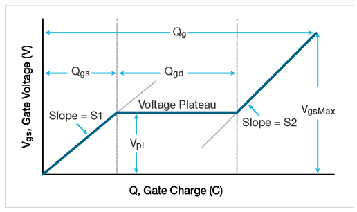
S1은 원점에서 첫 번째 평탄 지점까지의 선분의 기울기입니다. S2는 마지막 평탄 지점에서 지정된 최대 게이트 전압(VgsMax)까지의 선분의 기울기입니다. 기울기는 JESD24-2 표준에 명시된 것처럼 Qgs 및 Qgd를 계산하는 데 사용됩니다.

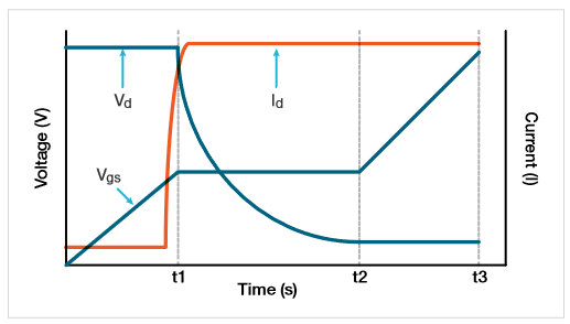
그림 2에는 일반 게이트 및 드레인 파형이 시간의 함수로 나와 있습니다. 게이트로 전류가 강제 주입되면 Vgs는 임계 전압에 도달할 때까지 증가합니다. 이 점에서 드레인 전류(Id)가 흐르기 시작합니다. 시간 t1에서 Cgs가 충전되면 Id는 일정하게 유지되고 드레인 전압(Vd)은 감소합니다. Vgs는 평탄 영역의 끝에 도달할 때까지 계속 일정하게 유지됩니다. 시간 t2에서 Cgd가 충전되면, 게이트-소스 전압(Vgs)이 지정된 최대 게이트 전압(VgsMax)에 도달할 때까지 다시 증가하기 시작합니다.

 
시간의 함수로 게이트와 드레인 파형을 보여주는 그래프
그림 2. Vgs, Vd, Id 대 MOSFET의 시간
 

4200A-SCS를 사용한 MOSFET 게이트 전하 측정

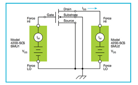
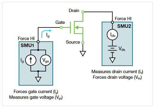
4200A-SCS는 두 개의 소스 측정 장치(SMU)를 사용해 파워 MOSFET의 게이트 전하를 측정합니다. 그림 3에는 게이트 전하 테스트의 기본 회로도가 나와 있습니다. 한 SMU(SMU1)의 강제 HI 단자를 MOSFET의 게이트 단자에 연결하고 게이트 전류(Ig)를 강제해 시간의 함수로 게이트-소스 전압(Vgs)을 측정합니다. 두 번째 SMU(SMU2)는 고정된 전압(Vds)을 지정된 전류 컴플라이언스 상태(Ib)에서 드레인에 인가합니다. 4200-SMU의 최대 컴플라이언스 전류는 0.1A이고, 4210-SMU의 최대 컴플라이언스 전류는 1A입니다.

게이트 전하를 테스트할 때는 게이트 전압이 증거하고 트랜지스터가 켜집니다. 평탄 영역에서 이러한 전환 중에는 전류가 지정된 컴플라이언스 레벨을 초과하기 때문에 드레인 SMU(SMU2)가 전압 제어에서 전류 제어 모드로 전환됩니다. 소프트웨어는 OFF 상태에서 ON 상태로 전환하는 동안 드레인 전류 과도 특성과 드레인 전압을 반환합니다.

MOSFET의 소스 단자는 4200A-SCS 섀시의 강제 LO 단자나 GNDU에 연결됩니다.

 
두 대의 소스 측정 장치(SMU)를 사용한 MOSFET 게이트 전하 테스트 구성
그림 3. 두 대의 SMU를 사용한 게이트 전하 테스트 구성.
 

MOSFET 게이트 전하 측정을 위한 Clarius+ 소프트웨어 구성

게이트 전하 테스트는 검색창에서 "게이트 전하"라는 문구를 검색하면 테스트 라이브러리와 프로젝트 라이브러리에서 모두 찾을 수 있습니다. 테스트 라이브러리에서 테스트를 찾으면 테스트를 선택해 프로젝트 트리에 추가함으로써 프로젝트를 추가할 수 있습니다. GateCharge 사용자 라이브러리의 gate_charge 사용자 모듈에서 생성되었습니다.

입력 매개변수 입력

테스트 실행 전 Clarius 소프트웨어의 구성창에서 입력 테스트 매개변수를 입력해야 합니다. (그림 4) 입력 매개변수는 장치와 사용하는 소스 측정 장치(SMU)에 따라 달라집니다.

 
Keithley Clarius 소프트웨어의 구성 보기에서 MOSFET 게이트 전하 테스트 설정
그림 A4. 구성 보기의 게이트 전하 테스트.
 

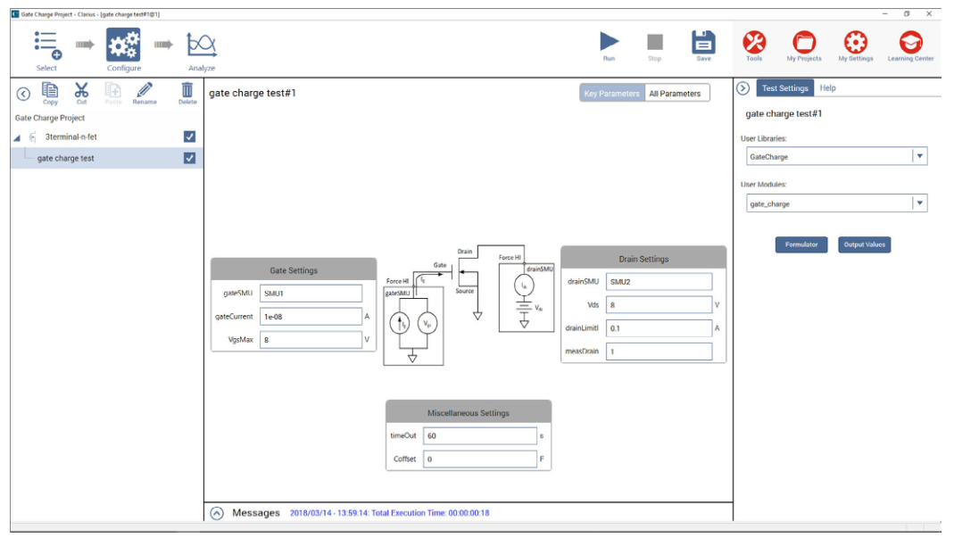
입력 매개변수에 대한 설명은 표1에 나와 있습니다. 먼저 MOSFET의 게이트(gateSMU)와 드레인(drainSMU)에 연결된 SMU 수를 입력합니다. 소스 단자는 항상 GNDU 또는 강제 LO에 연결되어야 합니다.

gateSMU에 의해 게이트로 강제 주입되는 전류의 크기는 gateCurrent(Ig) 매개변수입니다. 드레인 전압(Vds)은 드레인에 인가된 바이어스 전압이며 drainLimitI는 드레인 SMU의 컴플라이언스 전류입니다.

Coffset 매개변수는 오프셋 커패시턴스를 보정하는 데 사용되며 다음 단락에서 설명됩니다.

표 1. gate_charge 사용자 모듈용 입력 매개변수

입력 매개변수 값의 범위 기본값 설명
gateSMU SMU1-SMU9 SMU1 게이트 단자에 연결된 SMU 수
drainSMU SMU1-SMU9 SMU2 드레인 단자에 연결된 SMU 수
소스 GNDU GNDU 소스 단자는 항상 GNDU의 강제 LO 단자에 연결됨
Vds ±200V 10V 드레인 SMU의 드레인 바이어스 전압 크기
drainLimitI 4200-SMU: 0.1A
4210-SMU: 1A
0.1A 드레인 SMU의 전류 컴플라이언스
gateCurrent ±1E-5A 1e-7A 게이트 SMU의 게이트 전류 크기
VgsMax ±200V 10V 게이트 SMU의 최대 전압 레벨
타임아웃 0~300초 60초 시간 초과 전 시간(초)
measDrain 1(예)/0(아니오) 1 반환 측정 드레인 전류
Coffset 0 또는 Ceff 0 개방 회로로 테스트 실행 후 시트에 반환된 Ceff 값을 입력


오프셋 커패시턴스 보정

측정 시스템의 케이블 연결 및 연결에 따라 오프셋 커패시턴스는 단일 피코패럿에서 수백 피코패럿 범위가 될 수 있습니다. 이러한 커패시턴스는 개방 회로로 gate_charge 사용자 모듈을 실행하여 오프셋 커패시턴스를 구한 다음 소프트웨어에 오프셋 커패시턴스 값을 입력하여 보정할 수 있습니다. 이러한 단계를 수행하는 방법은 다음과 같습니다.

  1. 오프셋 커패시턴스를 측정합니다. 장치가 SMU에 연결된 것처럼 입력 게이트 전류 등의 테스트 매개변수를 설정합니다. (Ceff 측정을 위해 VgsMax를 증가시킵니다.) 테스트를 실행하기 전 프로브를 들어올리거나 테스트 픽스쳐에서 장치를 제거합니다. 개방 회로로 게이트 전하 테스트를 실행합니다.
  2. 오스셋 커패시턴스를 구합니다. 테스트가 실행되고 나면 측정된 시스템 오프셋 커패시턴스가 계산되어 시트의 Ceff 열에 표시됩니다. Ceff는 최대 게이트 전압, 게이트 전류 및 시간에서 도출됩니다.
    이 단계에서 개방 회로가 측정되기 때문에 테스트가 실행되고 나면 시트에 테스트 상태값 -9 또는 -12가 표시될 수 있습니다. 이는 측정된 장치가 없어 평탄 영역이 없기 때문입니다. 하지만 Ceff 값은 올바르며 구성 보기에서 Coffset으로 입력할 수 있습니다.
  3. 측정된 오프셋 커패시턴스를 입력하고 실행합니다. 구성 보기의 Coffset에 측정된 오프셋 커패시턴스, Ceff를 입력합니다. 기본적으로 Coffset는 0F입니다. 오프셋 커패시턴스에 대한 보상은 다음 판독값에서 이루어집니다.

테스트 실행

입력 매개변수를 입력했으면 화면 상단의 실행을 선택해 테스트를 실행합니다. 테스트가 실행되는 동안 분석 보기에 있는 그래프에 실시간으로 게이트 전하 파형이 업데이트되고 계산된 출력 매개변수가 시트에 표시됩니다.

출력 매개변수 보기

테스트가 완료되면 시트에 여러 매개변수가 반환됩니다. 표 2에는 이러한 매개변수에 대한 설명이 나와 있습니다.

표 2. gate_charge 사용자 모듈용 출력 매개변수

 
출력 매개변수 설명
gate_charge 테스트 상태값 - 설명은 표3 참조
timeArray 측정된 시간(초)
VgArray 측정된 게이트-소스 전압(볼트)
VgCharge 측정된 게이트 전하(쿨롬)
VdArray 측정된 드레인 전압(볼트)
IdArray 측정된 드레인 전류(암페어)
기울기 게이트 전압의 동적 기울기(dVg/dt)
Ceff 최대 게이트 전압에 대한 게이트 전하 비율
Vpl 평탄 또는 밀러 전압(볼트)
T1 평탄부가 시작되는 타임스탬프(초)
T2 평탄부가 끝나는 타임스탬프(초)
Qgs 원점에서 첫 번째 변곡점, 또는 전압 평탄부까지의 게이트 전하(쿨롬)
Qgd 게이트 전하 곡선의 두 변곡점 사이의 게이트 전하(쿨롬)
Qg 원점에서 VgsMax까지의 게이트 전하(쿨롬)


결과를 그래프로 나타내기

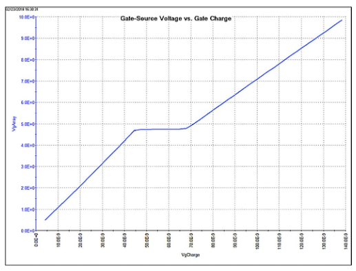
결과 게이트-소스 전압은 게이트 전하 또는 드레인 전류의 함수로 도시할 수 있으며 드레인 전압은 시간의 함수로 도시할 수 있습니다. 그림 5는 4200A-SCS에서 생성되는 일반적인 게이트 전압 파형입니다.

 
Keithley 4200A-SCS 파라미터 분석기에서 생성된 MOSFET 게이트 전압 파형
그림 5. 4200A-SCS에서 생성된 일반 게이트 전압 파형.
 

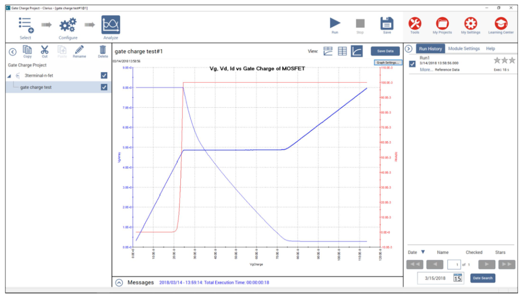
Vgs, Vds 외에도 Id 또한 MOSFET 게이트 전하 또는 시간의 함수로 도시할 수 있습니다. 그림 6에서는 Clarius 소프트웨어의 분석 보기 내 그래프에서 세 개의 매개변수가 모두 게이트 전하의 함수로 도시되는 모습을 보여줍니다. 이러한 경우 전압은 Y1 축에 표시되고 전류는 Y2 축에 도시됩니다.

 
시간 경과에 따른 MOSFET 게이트 전하 함수로서의 Vgs, Vds, 및 Id
그림 6. 게이트 전하 함수로서의 Vgs, Vds, Id.
 

테스트 상태 확인하기

테스트가 실행될 때마다 테스트 상태 값이 시트의 첫 번째 열("gate_charge")에 반환됩니다. 표 3에는 "gate_charge" 열에 반환된 테스트 상태 값과 그에 관한 설명 및 참고 사항이 나열되어 있습니다.

표 3. 테스트 상태 값

테스트 상태 설명 참고
1 오류 없음 테스트가 성공적으로 수행되었습니다.
-1 게이트 SMU가 존재하지 않음 올바른 SMU를 지정하십시오.
-2 드레인 SMU가 존재하지 않음 올바른 SMU를 지정하십시오.
-3 VgsMax > 200V 게이트 전압이 200V 미만인지 확인합니다. 게이트 전압을 줄이십시오.
-4 드레인 전류 한계 초과 1A (4210-SMU)
드레인 전류 한도 초과 0.1A(4200-SMU)
드레인 전류가 1A(중간 전력 SMU의 경우 0.1A) 미만인지 확인합니다. 드레인 전류 한도(drainLimitI)를 줄입니다.
-5 전력 한도가 초과됨 전압이 20V보다 크다면 전류는 0.1A 미만이어야 합니다. 드레인 전류 한도(drainLimitI)를 줄이거나 드레인 전압(Vds)을 낮춥니다.
-6 입력 조건의 오류 확인. timeOut을 200초로 제한 timeOut을 200초 미만으로 지정하십시오.
-7 테스트 시간이 지정한 시간을 초과함(timeOut) timeOut을 늘리십시오. 최대 시간은 200초입니다. 장치 충전 속도를 높이려면 gateCurrent를 높이십시오.
-8 반복/측정 횟수 >10,000 게이트 전류(gateCurrent)를 늘립니다.
-9 반복/측정 횟수 <5 게이트 전류(gateCurrent)를 줄입니다. 장치, 테스트 설정을 확인하고, 올바른 SMU인지 확인합니다.
이 오류가 오프셋 보정을 위해 개방 회로를 측정하는 동안 발생했다면 무시해도 됩니다. Ceff 값은 여전히 유효합니다.
-10 원점에서 첫 번째 평탄 지점까지의 지점 수 <10 게이트 전류(gateCurrent)를 줄입니다.
-11 기울기 S1 계산 오류. 상관 계수 <0.9. 원점에서 첫 번째 평탄 지점까지의 곡선이 선형이 아님. 장치와 테스트 설정을 확인합니다.
-12 기울기 S2 계산 오류. 상관 계수 0.9 미만. 마지막 평탄 지점에서 VgsMax까지의 곡선이 선형이 아님. 장치와 테스트 설정을 확인합니다. VgCharge 또는 VdArray가 높게 나타나면 gateCurrent를 낮추고 테스트를 반복하십시오.
이 오류가 오프셋 보정을 위해 개방 회로를 측정하는 동안 발생했다면 무시해도 됩니다. Ceff 값은 여전히 유효합니다.
-13 Vds > 200V 드레인 전압을 낮춥니다.
-14 gateCurrent > 10µA 게이트 전류(Ig)를 줄입니다.


결론

Keithley 4200A-SCS 파라미터 분석기를 사용하면 트랜지스터에서 MOSFET 게이트 전하를 쉽게 측정할 수 있습니다. Clarius 소프트웨어는 장치의 게이트와 드레인에 연결된 두 대의 SMU를 사용해 쉽게 게이트 전하 파형을 도출합니다.

TEK.COM에서 더 유용한 리소스 찾기

리소스

fig-18
브로슈어

레이더에 대한 실제 신호 만들기

가장 높은 주파수에서 복잡한 레이더 테스트 신호를 만들 수 있는 최적의 솔루션은 무엇일까요? 텍트로닉스 앱은 레이더 시스템의 교란 신호를 만드는 최고의 방법을 다룹니다.

smu
블로그

고급 레이더 분석: 최신 레이더 측정용 도구

설계 과정 중 테스트 불확실성을 줄이고 점점 더 복잡해지는 설계에 확신을 제공합니다. 텍트로닉스의 노트는 최신 레이더에 필요한 도구를 보여줍니다.

SMU Group
블로그

전자 보호 대책 검증 기술

이 웨비나에서는 RSA5100B 및 RSA7100과 같은 텍트로닉스의 실시간 스펙트럼 분석기를 사용하여 전자 보호 대책(ECM) 시스템을 검증할 접근 방식을 살펴봅니다.

Noisey gate drive
블로그

전자 보호 대책 검증 기술

이 웨비나에서는 RSA5100B 및 RSA7100과 같은 텍트로닉스의 실시간 스펙트럼 분석기를 사용하여 전자 보호 대책(ECM) 시스템을 검증할 접근 방식을 살펴봅니다.

Mosfet Gate Charge Frequently Asked Questions

What is the drain-source on-resistance of a MOSFET?

MOSFET switching devices operate in the on and off states. In the “on” state, the impedance of the switch is theoretically zero and no power is dissipated in the switch no matter how much current is flowing through it. In the “off” state, the impedance of the switch is theoretically infinite, therefore no current is flowing and no power is dissipated.

Thedrain-source on-resistance (RDS(on)) is the effective resistance between the drain and the source of a MOSFET when it’s in the on state. This occurs when a specific gate-to-source voltage (VGS) is applied. In general, as the VGS increases, the on-resistance decreases. The lower the MOSFET on-resistance, the better because a low resistance reduces undesired power dissipation, improving the power efficiency of the device.

How can I test a MOSFET for drain-source on-resistance on my curve tracer?

Answer: Drain-Source On-Resistance - RDS(on)

What is drain-source on-resistance?

Drain-source on-resistance (RDS(on)) is the resistance between the drain and the source of a MOSFET when a specific gate-to-source voltage (VGS) is applied to bias the device to the on state. As the VGS increases, the on-resistance generally decreases. The measurement is made in the ohmic (i.e. linear) region of the device. Generally speaking, the lower the MOSFET on-resistance, the better.

One of the ways to trace this resistance is to use a curve tracer. On a curve tracer, the so called “Collector Supply” drives the drain while the “Step Generator” drives the gate. For step-by-step instructions on how to test a MOSFET for drain-source on-resistance using a curve tracer, see below. For instructions on how to use an oscilloscope or SMU to measure MOSFET on-resistance, see our “What is the drain-source on-resistance of a MOSFET?” FAQ.

What the display shows:

The display shows VDS on the horizontal axis, and the resulting ID on the vertical axis. The specification is met when at the specified VDS, VDS/ID is less than or equal to the specified maximum.

How to test a MOSFET for drain-source on-resistance on a curve tracer:

1. Under Controls, set:

            A:Max Peak Volts to the lowest setting above the specified VDS

            B: Max Peak Power Watts to the lowest setting that satisfies (ID x VDS)

            C: Collector Supply Polarity to (+DC) for N-channel or (-DC) for P-channel  

            D: Horizontal Volts/Div to display VDS between the 5th and 10th horizontal divisions

            E: Vertical Current/Div to display ID between the 5th and 10th vertical divisions

            F: Number of steps to minimum (zero)

            G: Step Generator to Voltage

            H: Step Generator Polarity to apply forward bias (+ for N-channel), (- for P-channel)

            I: Step/Offset Ampl to approx 50% of the specified VGS

            J: Pulse to Long       

            K: Configuration to (Base/Step Gen, Emitter/Common)

            L: Variable Collector Supply to minimum % (full ccw)

            M: DotCursor ON

2. Apply power to the MOSFET:

            A: Position the Left/Right switch as appropriate

            B: Slowly increase the Variable Collector Supply until the specified VDS is reached

3. Compare to data sheet specifications:

            A: Check that VDS/ID is less than or equal to the specified minimum

Tektronix Curve Tracers are discontinued products. More efficient and accurate methodologies and solutions have been designed to support curve tracing functionality on a much more compact form factor. One such solution is based on using a dual channel SMU or two single channel SMUs and software to control the bias voltage step generation and the relative drain to source voltage drop. To learn more, see our “What is the drain-source on-resistance of a MOSFET?” FAQ.

How do you find the transconductance of a MOSFET?

Transconductance is a key test for validating the MOSFET performance in power electronics designs. It ensures that a MOSFET is functioning properly and helps engineers choose the best one when voltage gain is a key spec for their circuit designs. This, in turn allows companies to take power semiconductor devices to market faster while minimizing failures in the field.

Transconductance is the ratio of drain current (ID) to gate-source voltage (VGS) when a constant drain-source voltage is applied. The current to voltage ratio is commonly referred to as gain. Transconductance is a critical parameter strictly connected with the threshold voltage (VTH) of MOSETs and both are related to the size of the gate channel. The formula for deriving the transconductance of a MOSFET from I-V measurements is:

gm = ΔID / ΔVGS

How to measure transconductance of a MOSFET?

The approach shown in the first configuration calls for three source measure units (SMUs), allowing every node to be held at a feedback-controlled voltage and every current to be measured simultaneously. If you don’t have enough SMU channels to cover each device channel connection, it is possible to proceed as shown in the second configuration. It should be noted that this configuration is more susceptible to a noisy ground connection and can produce ground loops if long cables are used. Also, the current and voltage at the source terminal cannot be measured, which can lead to errors in calculations.

Measuring transconductance

  1. Sweep the gate voltage (VGS) over the desired range, while maintaining a constant drain/source voltage (VDS)
  2. Measure the drain current (ID) at each increment step of VGS.
  3. Calculate transconductance (gm) by dividing the small changes in the current ID by the small changes in VGS.

The red plot line shown here illustrates the transconductance (gm) and the maximum transconductance value (Vth).

Learn more about safe, precise and fast MOSFET device characterization tests.

How can I test a MOSFET for Zero Gate Voltage Drain Current on my curve tracer?

Answer: Zero Gate Voltage Drain Current - IDSS

What is Zero Gate Voltage Drain Current? 

Zero gate voltage drain current is the ID that flows when VGS=0.  It’s the on-state current in a depletion mode MOSFET and the off-state current in an enhancement mode MOSFET.

On the IV curve tracer, the Collector Supply drives the drain and the gate is shorted to the source so that VGS=0.

What The Display Shows:

The display shows VDS on the horizontal axis, and the resulting ID on the vertical axis.  The specification is met when with VGS=0 and the specified VDS applied, ID is less than or equal to the specified maximum.

How To Do It:

1. Set controls:

            A:Max Peak Volts to the lowest setting above the specified VDS

            B: Max Peak Power Watts to the lowest setting that satisfies (ID x VDS)

            C: Horizontal Volts/Div to display VDS between the 5th and 10th horizontal divisions

            D: Vertical Current/Div to display the ID between the 5th and 10th vertical divisions

            E: Collector Supply Polarity to (+DC) for N-channel or (-DC) for P-channel

            F: Configuration to (Base/Short, Emitter/Common)

            G: Variable Collector Supply to minimum % (full ccw)

            H: DotCursor ON

2. Apply power to the MOSFET:

            A: Position the Left/Right switch as appropriate

            B: Slowly increase the Variable Collector Supply % until the specified VDS is reached

3. Compare to data sheet specifications:

            Check that at the specified VDS, ID is less than or equal to the specified maximum

How can I test a MOSFET for Gate Threshold Voltage on my curve tracer?

Answer: Gate Threshold Voltage - VGS(th)

What is Gate Threshold Voltage? 

Gate threshold voltage is the lowest VGS at which a specified small amount of ID flows.  The test is run with VGS = VDS.

On the curve tracer, the Collector Supply provides VDS.  Patch cords are used to short the gate to the drain so that VGS=VDS.

What The Display Shows:

VGS is displayed on the horizontal axis, and the resulting ID is displayed on the vertical axis.  The specification is met when, at the specified ID, VGS is within the min/max limits.

How To Do It:

1. Set controls:

            A: Max Peak Volts to the lowest setting above the specified VGS

            B: Max Peak Power Watts to the lowest setting that satisfies (ID x VDS)

            C: Horizontal Volts/Div to display VGS between the 5th and 10th horizontal divisions

            D: Vertical Current/Div to display the specified  ID between the 5th and 10th vertical divisions

            E: Collector Supply Polarity to (+DC) for N-channel or (-DC) for P-channel

            F: Configuration to (Base/Open, Emitter/Common)

            G: Variable Collector Supply to minimum % (full ccw)

            H: DotCursor ON

2: Attach patch cords:

            A: Connect a patch cord between the base and collector terminals on the unused side of the interface area

            B: Connect a second patch cord between the base sense and collector sense terminals on the unused side of the fixture area

3. Apply power to the MOSFET:

            A: Position the Left/Right switch to Both

            B: Slowly increase the Variable Collector Supply % until either the specified ID or the maximum threshold voltage is attained – whichever comes first

4. Compare to data sheet specifications:

            Check that the gate threshold voltage is within the specified min/max limits

How can I test a MOSFET for Transconductance (gFS) and Forward Admittance on my curve tracer?

Answer: Transconductance (gFS) and Forward Admittance

What is Transconductance and Forward Admittance? 

Transconductance is the ratio of ID to VGS.  The I/V ratio is commonly referred to as gain.

On the curve tracer, the Collector Supply drives the drain and the Step Generator drives the gate.

What The Display Shows:

The display shows VDS on the horizontal axis, and the resulting ID on the vertical axis.  With the Step Generator providing gate drive, the curve will be displaced upward from the horizontal axis as the gate drive causes a proportional ID.  The specification is met when, at either the specified VGS or the specified ID, the ratio of ID to VGS is equal to or greater than the specified minimum.

How To Do It:

1. Set controls:

            A:Max Peak Volts to the lowest setting above the specified VDS

            B: Peak Power Watts at the lowest setting to satisfy (ID x VDS)

            C: Collector Supply Polarity to (+DC) for N-channel or (-DC) for P-channel

            D: Horizontal Volts/Div to display the specified VDS between the 5th and 10th horizontal divisions

            E: Vertical Current/Div to display the specified ID between the 5th and 10th vertical divisions

            F: Number of steps to minimum (zero)

            G: Step Generator to Voltage

            H: Step Generator Polarity to apply forward bias  (+ for N-channel),  (- for P-channel)

            I: Step/Offset Ampl to approx 1% of the specified VDS

            J: Pulse to Long       

            K: Configuration to (Base/Step Gen, Emitter/Common)

            L: Variable Collector Supply to minimum % (full ccw)

            M: DotCursor ON

2. Apply power to the MOSFET:

            A: Position the Left/Right switch as appropriate

            B: Slowly increase the Variable Collector Supply % until the specified  VDS is reached

3. Adjust to parameters:

            Press and hold Offset Aid until an appreciable vertical displacement of the   curve occurs. It will be necessary to readjust Variable Collector % to maintain VDS.  Continue adjusting Step Offset and VDS alternately until the specified operating point is reached.

4. Calculate transconductance (gFS):

             Read gFS directly from the cursor readout

5. Compare to data sheet specifications:

              Check that the value is equal to or greater than the specified minimum

Forward admittance is an alternative way of expressing transconductance and is measured by setting the curve tracer up to measure transconductance (as above), switching Horizontal Volts/Div to STEP GEN, using SWEEP to complete the curve, then changing the cursor to F line and positioning the slope of the F line until it’s tangent to the curve.

How can I test a MOSFET for On-State Drain Current on my curve tracer?

Answer: On-State Drain Current - ID(on)

What is On-State Drain Current?

On-state drain current is ID with a specified VGS to bias the device to the on-state.  The measurement is made in the ohmic (i.e. linear) region of the device.

On the curve tracer the Collector Supply drives the drain and the Step Generator drives the gate.

What The Display Shows:

The display shows VDS on the horizontal axis, and the resulting ID on the vertical axis.  The specification is met when at the specified VDS, ID is greater than or equal to the specified minimum.

How To Do It:

1. Set controls:

            A:Max Peak Volts to the lowest setting above the specified VDS

            B: Max Peak Power Watts to the lowest setting that satisfies (ID x VDS)

            C: I: Collector Supply Polarity to (+DC) for N-channel or (-DC) for P-channel  

            D: Horizontal Volts/Div to display VDS between the 5th and 10th horizontal divisions

            E: Vertical Current/Div to display ID between the 5th and 10th vertical divisions

            F: Number of steps to minimum (zero)

            G: Step Generator to Voltage

            H: Step Generator Polarity to apply forward bias (+ for N-channel),  (- for P-channel)

            I: Step/Offset Ampl to approx 50% of the specified VGS

            J: Pulse to Long       

            K: Configuration to (Base/Step Gen, Emitter/Common)

            L: Variable Collector Supply to minimum % (full ccw)

            M: DotCursor ON

2. Apply power to the device:

            A: Position the Left/Right switch as appropriate

            B: Slowly increase the Variable Collector Supply until the specified VDS is reached

3. Compare to data sheet specifications:

            A: Check that ID is equal to or greater than the specified minimum

How can I test a MOSFET for drain-source breakdown voltage on my curve tracer?

Answer: Drain-Source Breakdown Voltage - V(br)DSS

What is Drain-Source Breakdown Voltage?

Drain-source breakdown voltage is the VDS at which a specified value of ID flows, with VGS=0.  Since it's the reverse current through a pinched-off channel, ID exhibits a knee shaped rise, increasing rapidly once breakdown occurs.

On the curve tracer, the Collector Supply drives the drain and the gate is shorted to the source so VGS=0.

What The Display Shows:

The display shows VDS on the horizontal axis, and the resulting ID on the vertical axis.  The specification is met when, at the specified ID, VDS is greater than or equal to the specified minimum.

How To Do It:

1. Set controls:

A: Max Peak Volts to the lowest setting above the specified minimum

     VDS

            B: Max Peak Power Watts to the lowest setting that satisfies (ID x VDS)

            C: Horizontal Volts/Div to display VDS between the 5th and 10th horizontal divisions

            D: Vertical Current/Div to display ID between the 5th and 10th vertical divisions                  

            E: Collector Supply Polarity to +Leakage (for N-channel) or -Leakage (for P-channel)

            F: Configuration to (Base/Short, Emitter/Common)

            G: Variable Collector Supply to minimum % (full ccw)

            H: DotCursor ON

2. Apply power to the MOSFET:

            A: Position the Left/Right switch as appropriate

            B: Slowly increase the Variable Collector Supply % until the specified ID is attained

3. Compare to data sheet specifications:

            Check that at the specified ID, VDS is greater than or equal to the specified minimum

How can I test a MOSFET for Forward Gate Body Leakage Current on my curve tracer?

Answer: Zero Gate Voltage Drain Current - IDSS

What is Zero Gate Voltage Drain Current?

Zero gate voltage drain current is the ID that flows when VGS=0.  It’s the on-state current in a depletion mode MOSFET and the off-state current in an enhancement mode MOSFET.

On the curve tracer, the Collector Supply drives the drain and the gate is shorted to the source so that VGS=0.

What The Display Shows:

The display shows VDS on the horizontal axis, and the resulting ID on the vertical axis.  The specification is met when with VGS=0 and the specified VDS applied, ID is less than or equal to the specified maximum.

How To Do It:

1. Set controls:

            A:Max Peak Volts to the lowest setting above the specified VDS

            B: Max Peak Power Watts to the lowest setting that satisfies (ID x VDS)

            C: Horizontal Volts/Div to display VDS between the 5th and 10th horizontal divisions

            D: Vertical Current/Div to display the ID between the 5th and 10thvertical divisions

            E: Collector Supply Polarity to (+DC) for N-channel or (-DC) for P-channel

            F: Configuration to (Base/Short, Emitter/Common)

            G: Variable Collector Supply to minimum % (full ccw)

            H: DotCursor ON

2. Apply power to the MOSFET:

            A: Position the Left/Right switch as appropriate

            B: Slowly increase the Variable Collector Supply % until the specified VDS is reached

3. Compare to data sheet specifications:

            Check that at the specified VDS, ID is less than or equal to the specified maximum