Current Language
×
Chinese (Traditional, Taiwan)

選取語言:

切換功能表
Current Language
×
Chinese (Traditional, Taiwan)

選取語言:

與我們聯絡

與 Tek 業務代表即時對談。 上班時間:上午 6:00 - 下午 4:30 (太平洋時間)

致電

請致電

與 Tek 業務代表即時對談。 上班時間:上午 8:30 - 下午 5:30 (太平洋時間)

下載

下載手冊、產品規格表、軟體等等:

下載類型
機型或關鍵字

意見回饋

使用 4200A-SCS 參數分析儀進行 MOSFET 閘級電荷量測


簡介

功率 MOSFET 用於多種應用,並可作為高速開關使用。裝置的開關速度受內部電容影響,內部電容通常在產品規格表中以 Ciss 和 Coss 指定,其從輸入閘級和汲極電容 Cgs 和 Cgd 得出。除了指定電容以外,閘級電荷 (Qgs 和 Qgd) 也可用於評估 MOSFET 的開關效能。

JEDEC JESD24-2 標準「閘級電荷測試方法」中說明了一種測量 MOSFET 閘級電荷的方法。透過此方法可強制施加閘級電流,同時將閘級至源極電壓測量為時間的函數。從產生的閘級電壓波形中,可得出閘級-源極電荷 (Qgs)、閘級-汲極電荷 (Qgd) 和閘級電荷 (Qg)。

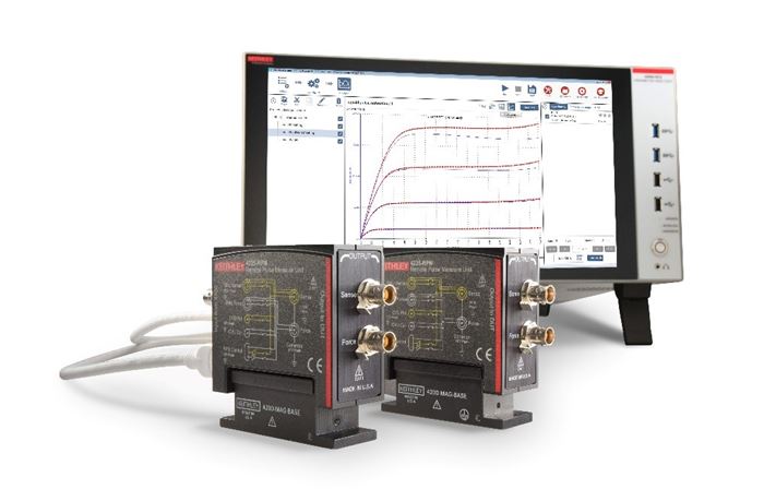
4200A-SCS 參數分析儀支援使用兩部電源量測設備 (SMU) 儀器和系統中包含的閘級電荷測量測試來進行 MOSFET 閘級電荷測量。該測試是 4200A-SCS Clarius+ 軟體套件中提供的廣泛測試庫中所包含的眾多測試之一。本應用摘要說明如何使用 4200A-SCS 參數分析儀根據 JEDEC 閘級電荷測試方法測量 MOSFET 閘級電荷。

MOSFET 閘級電荷測量概觀

在閘級電荷方法中,將固定測試電流 (Ig) 強制流入 MOS 的閘級,便會根據流入閘級的電荷繪製電晶體與測得的閘級源極電壓 (Vgs)。會向汲極端子供應固定電壓偏壓。圖 1 顯示了功率 MOSFET 的閘級電壓相對於閘級電荷。

閘級電荷 (Q) 強制閘級電流與時間 (Igdt) 得出。如圖 1 所示,閘級-源極電荷 (Qgs) 是到達電壓 (Vgs) 幾乎恆定的高原區域開始處所需的電荷。根據 JEDEC 標準,高原 (或米勒) 電壓 (Vpl) 定義為 dVgs/dt 最小時的閘極-源極電壓。電壓高原是電晶體從關斷狀態切換到導通狀態時的區域。完成此切換所需的閘級電荷—將裝置從高原區域的開始處切換到結束所需的電荷—定義為閘級-汲極電荷 (Qgd),其稱為米勒電荷。閘級電荷 (Qg) 是從原點到閘級源極電壓 (Vgs) 等於指定最大值 (VgsMax) 之點的電荷。

 
顯示功率 MOSFET 的閘級電壓相對於閘級電荷的 MOSFET 閘級電荷測量圖
圖 1. 功率 MOSFET 的典型閘級電壓相對於閘級電荷。
 

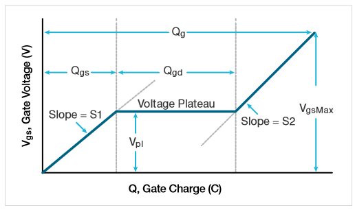
S1 是從原點到第一個高原點之線段的斜率。S2 是從最後一個高原點到指定最大閘級電壓 (VgsMax) 之線段的斜率。這些斜率用於計算 Qgs 和 Qgd,如 JESD24-2 標準所指定。

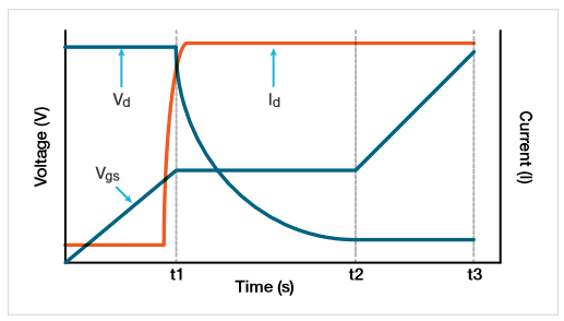
圖 2 將典型閘級和汲極波形顯示為時間的函數。當電流被迫流向閘級時,Vgs 會增加,直到達到臨界值電壓為止。在這一點,汲極電流 (Id) 開始流動。當 Cgs 在時間 t1 充電時,Id 會保持恆定,汲極電壓 (Vd) 會降低。Vgs 會保持恆定,直到到達高原結束為止。當 Cgd 在時間 t2 充電時,閘極-源極電壓 (Vgs) 會再次開始增加,直到達到指定的最大閘極電壓 (VgsMax) 為止。

 
將閘級和汲極波形顯示為時間函數的圖形
圖 2. Vgs、Vd 與 Id 相對於 MOSFET 的時間
 

使用 4200A-SCS 進行 MOSFET 閘級電荷測量

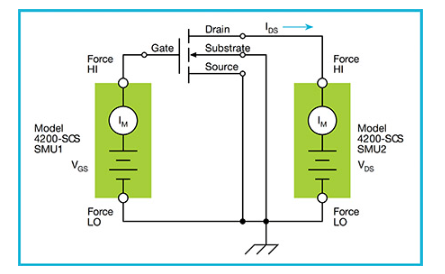
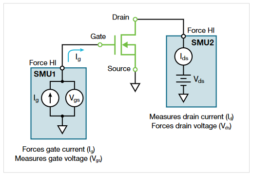
4200A-SCS 使用兩個 SMU 儀器測量功率 MOSFET 的閘級電荷。圖 3 顯示了閘級電荷測試的基本電路圖。一個 SMU (SMU1) 的強制 HI 端子連接到 MOSFET 的閘級端子,強制閘級電流 (Ig) 並將閘級-源極電壓 (Vgs) 測量為時間的函數。第二個 SMU (SMU2) 以指定的電流相容性 (Ib) 將固定電壓 (Vds) 供應到汲極。4200-SMU 的最大相容性電流為 0.1 A;4210-SMU 的最大相容性為 1 A。

在閘級電荷測試期間,閘級電壓會增加並導通電晶體。在高原區域的這個轉換期間,汲極 SMU (SMU2) 會從電壓控制切換到電流控制模式,因為電流超過了指定的相容性層級。軟體會在轉換期間將汲極電流暫態與汲極電壓從關斷狀態恢復到導通狀態。

MOSFET 的源極端子連接到 4200A-SCS 底盤的強制 LO 端子或 GNDU。

 
使用兩部電源量測設備 (SMU) 儀器的 MOSFET 閘級電荷測試組態
圖 3. 使用兩部 SMU 儀器的閘級電荷測試組態。
 

設定 Clarius+ 軟體進行 MOSFET 閘級電荷測量

閘級電荷測試位於測試庫和專案庫中,可以透過搜尋片語「閘級電荷」在「選取」窗格中找到它們。在測試庫中找到測試後,可以透過選取並將其新增至專案工作流程來將其新增至專案。此測試是從 GateCharge 使用者庫中的 gateway_charge 使用者模組建立的。

輸入輸入參數

在執行測試之前,您需要在 Clarius 軟體的「設定」窗格中輸入輸入測試參數 (圖 4)。輸入參數將根據裝置和使用的 SMU 機型而有所不同。

 
在 Keithley Clarius 軟體的組態檢視中設定 MOSFET 閘級電荷測試
圖 4. 設定檢視中的閘級電荷測試。
 

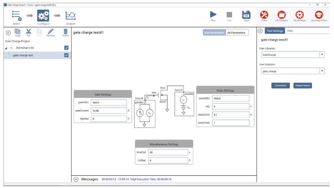
輸入參數的說明如表 1 所列。首先,輸入連接到 MOSFET 之閘級 (gateSMU) 和汲極 (drainSMU) 的 SMU 編號。源極端子應一律連接至 GNDU 或強制 LO。

由 gateSMU 強制流向閘級的電流振幅是 gateCurrent (Ig) 參數。汲極電壓 (Vds) 是供應到汲極的偏差電壓,drainLimitI 是汲極 SMU 的相容性電流。

Coffset 參數用於修正偏移電容,並在以下段落中說明。

表 1. gateway_charge 使用者模組的輸入參數。

輸入參數 值範圍 預設值 說明
gateSMU SMU1-SMU9 SMU1 連接到閘級端子的 SMU 編號
drainSMU SMU1-SMU9 SMU2 連接到汲極端子的 SMU 編號
訊號源 GNDU GNDU 源極端子一律連接到 GNDU 上的強制 LO 端子
Vds ±200 V 10 V 汲極 SMU 之汲極偏差電壓的振幅
drainLimitI 4200-SMU:0.1A
4210-SMU:1 A
0.1 A 汲極 SMU 的電流相容性
gateCurrent ± 1E-5 A 1e-7 A 閘級 SMU 之閘級電流的振幅
VgsMax ±200V 10 V 閘級 SMU 的最大電壓位準
逾時 0 至 300 s 60 s 逾時前的秒數。
measDrain 1 (是) 或 0 (否) 1 傳回測量的汲極電流
Coffset 0 或 Ceff 0 執行開路測試,然後輸入傳回規格表的 Ceff 值


修正偏移電容 

根據測量系統的佈線和連接,偏移電容可以在一微微法拉到數百微微法拉的範圍內。這些電容可以透過開路執行 gate_charge 使用者模組,獲得偏移電容,然後在軟體中輸入偏移電容值進行補償來修正。以下是執行這些步驟的方法:

  1. 測量偏移電容。設定測試參數,包括就像裝置已連接至 SMU 一樣輸入閘級電流。(僅針對 Ceff 測量增加 VgsMax。) 在執行測試之前,請提起探棒或從測試治具上取下裝置。以開路執行閘級電荷測試。
  2. 取得偏移電容。執行測試後,會計算系統的測量偏移電容並將其顯示在規格表的 Ceff 欄中。Ceff 從最大閘級電壓、閘級電流和時間得出。
    由於在此步驟中測量的是開路,因此執行測試後,規格表中可能會出現 -9 或 -12 的測試狀態值。這是因為沒有測量任何裝置,因此不存在高原區域。但是,Ceff 值是正確的,可以在設定檢視中輸入為 Coffset。
  3. 輸入測得的偏移電容並執行。在設定檢視中為 Coffset 輸入測得的偏移電容 Ceff。預設情況下,Coffset 為 0 F。將為後續讀數中的偏移電容進行補償。

執行測試

輸入輸入參數後,透過選取螢幕頂部的「執行」來執行測試。當測試正在執行中時,閘級電荷波形將會在分析檢視的圖形中即時更新,計算出的輸出參數將出現在規格表中。

檢視輸出參數

測試完成後,會將幾個參數傳回到規格表中。表 2 列出了這些參數的說明。

表 2. gateway_charge 使用者模組的輸出參數

 
輸出參數 說明
gate_charge 測試狀態值 - 如需說明,請參閱表 3
timeArray 測得的時間 (秒)
VgArray 測得的閘級-源極電壓 (伏特)
VgCharge 測得的閘級電荷 (庫侖)
VdArray 測得的汲極電壓 (伏特)
IdArray 測得的汲極電流 (安培)
斜率 閘級電壓的動態斜率 (dVg/dt)
Ceff 閘級電荷與最大閘級電壓的比
Vpl 高原或米勒電壓 (伏特)
T1 高原區域開始的時間戳記 (秒)
T2 高原區域結束的時間戳記 (秒)
Qgs 從原點到第一個轉折點的閘級電荷,或電壓高原 (庫侖)
Qgd 在閘級電荷曲線中的兩個轉折點之間的閘級電荷 (庫侖)
Qg 從原點到 VgsMax 的閘級電荷 (庫侖)


繪製結果

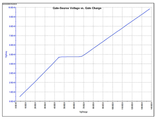
產生的閘級-源極電壓可以繪製為閘級電荷或汲極電流的函數,且汲極電壓可以繪製為時間的函數。圖 5 是 4200A-SCS 產生的典型閘級電壓波形

 
Keithley 4200A-SCS 參數分析儀產生的 MOSFET 閘級電壓波形
圖 5. 4200A-SCS 產生的典型閘級電壓波形。
 

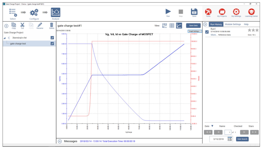
除了繪製 Vgs 外,還可以將 Vds 和 Id 繪製為 MOSFET 閘級電荷或時間的函數。圖 6 顯示了 Clarius 軟體分析檢視中的圖形,其中顯示了繪製為閘級電荷函數的全部三個參數。在此例中,電壓顯示在 Y1 軸上,電流繪製在 Y2 軸上。

 
Vgs、Vds 與 Id 作為 MOSFET 閘級電荷相對時間的函數
圖 6. Vgs、Vds 與 Id 作為閘級電荷的函數。
 

檢查測試狀態

每次執行測試時,測試狀態值都會傳回到規格表中的第一欄,名為「gate_charge」。表 3 列出了在「gate_charge」欄中傳回的測試狀態值及其對應說明與摘要。

表 3. 測試狀態值

測試狀態 說明 附註
1 沒有錯誤 測試成功。
-1 閘級 SMU 不存在 指定正確的 SMU。
-2 汲極 SMU 不存在 指定正確的 SMU。
-3 VgsMax > 200 V 驗證閘級電壓是否小於 200V。降低閘級電壓。
-4 汲極電流限制超過 1 A (4210-SMU)
汲極電流限制超過 0.1 A (4200-SMU)
驗證汲極電流是否小於 1 A (或對中等功率 SMU 為 0.1 A)。降低汲極電流限制 (drainLimitI)。
-5 超出功率限制 電流應為 < 0.1A if V >20V。降低汲極電流限制 (drainLimitI) 或汲極電壓 (Vds)。
-6 輸入條件錯誤檢查。將逾時限制為 200 秒。 將逾時指定為 <200 秒。
-7 測試時間超過指定逾時 (timeOut)。 增加逾時。最大值為 200 秒。嘗試增加 gateCurrent 以為裝置更快充電。
-8 迭代/測量次數 >10000。 增加閘級電流 (gateCurrent)。
-9 迭代/測量次數 <5 減少閘級電流 (gateCurrent)。檢查裝置、測試設定以獲得正確的 SMU。
如果在測量開路以進行偏移修正時發生此錯誤,則可忽略此錯誤。Ceff 值仍然有效。
-10 從原點到第一個高原點的點數 <10 減少閘級電流 (gateCurrent)
-11 計算斜率 S1 時發生錯誤。關聯係數 < 0.9。從原點到第一個高原點的曲線不是線性。 檢查裝置及測試設定。
-12 計算斜率 S2 時發生錯誤。關聯係數 < 0.9。從最後一個高原點到 VgsMax 的曲線不是線性。 檢查裝置及測試設定。如果 VgCharge 或 VdArray 偏高,請嘗試降低 gateCurrent 並重複測試。
如果在測量開路以進行偏移修正時發生此錯誤,則可忽略此錯誤。Ceff 值仍然有效。
-13 Vds > 200 V 減少汲極電壓。
-14 gateCurrent > 10 µA 減少閘級電流 (Ig)。


結論

使用 Keithley 4200A-SCS 參數分析儀可以輕鬆測量電晶體上的 MOSFET 閘級電荷。使用連接到裝置閘級與汲極的兩部 SMU 儀器,Clarius 軟體可以輕鬆導出閘級電荷波形。

前往 TEK.COM 尋找更多寶貴的資源

Related MOSFET Gate Charge Resources

fig-18
小冊子

建立類似於雷達的訊號

哪種最佳解決方案可協助您在最高頻率建立複雜的雷達測試訊號?我們的應用說明涵蓋了建立可以瞞過您雷達系統的訊號之最佳方法。

smu
部落格

進階雷達分析:現代雷達量測的工具

降低設計過程中的測試不確定性,並為日益複雜的設計建立信心。此應用摘要會一一解析,針對現代化的雷達時,您不可或缺的工具。

SMU Group
部落格

電子對抗的驗證技術

本次網路研討會探討了使用 Tektronix 即時頻譜分析儀 (例如 RSA5100B 和 RSA7100B),來驗證電子對抗 (ECM) 系統的方法。

Noisey gate drive
部落格

電子對抗的驗證技術

本次網路研討會探討了使用 Tektronix 即時頻譜分析儀 (例如 RSA5100B 和 RSA7100B),來驗證電子對抗 (ECM) 系統的方法。

Mosfet Gate Charge Frequently Asked Questions

What is the drain-source on-resistance of a MOSFET?

MOSFET switching devices operate in the on and off states. In the “on” state, the impedance of the switch is theoretically zero and no power is dissipated in the switch no matter how much current is flowing through it. In the “off” state, the impedance of the switch is theoretically infinite, therefore no current is flowing and no power is dissipated.

Thedrain-source on-resistance (RDS(on)) is the effective resistance between the drain and the source of a MOSFET when it’s in the on state. This occurs when a specific gate-to-source voltage (VGS) is applied. In general, as the VGS increases, the on-resistance decreases. The lower the MOSFET on-resistance, the better because a low resistance reduces undesired power dissipation, improving the power efficiency of the device.

How can I test a MOSFET for drain-source on-resistance on my curve tracer?

Answer: Drain-Source On-Resistance - RDS(on)

What is drain-source on-resistance?

Drain-source on-resistance (RDS(on)) is the resistance between the drain and the source of a MOSFET when a specific gate-to-source voltage (VGS) is applied to bias the device to the on state. As the VGS increases, the on-resistance generally decreases. The measurement is made in the ohmic (i.e. linear) region of the device. Generally speaking, the lower the MOSFET on-resistance, the better.

One of the ways to trace this resistance is to use a curve tracer. On a curve tracer, the so called “Collector Supply” drives the drain while the “Step Generator” drives the gate. For step-by-step instructions on how to test a MOSFET for drain-source on-resistance using a curve tracer, see below. For instructions on how to use an oscilloscope or SMU to measure MOSFET on-resistance, see our “What is the drain-source on-resistance of a MOSFET?” FAQ.

What the display shows:

The display shows VDS on the horizontal axis, and the resulting ID on the vertical axis. The specification is met when at the specified VDS, VDS/ID is less than or equal to the specified maximum.

How to test a MOSFET for drain-source on-resistance on a curve tracer:

1. Under Controls, set:

            A:Max Peak Volts to the lowest setting above the specified VDS

            B: Max Peak Power Watts to the lowest setting that satisfies (ID x VDS)

            C: Collector Supply Polarity to (+DC) for N-channel or (-DC) for P-channel  

            D: Horizontal Volts/Div to display VDS between the 5th and 10th horizontal divisions

            E: Vertical Current/Div to display ID between the 5th and 10th vertical divisions

            F: Number of steps to minimum (zero)

            G: Step Generator to Voltage

            H: Step Generator Polarity to apply forward bias (+ for N-channel), (- for P-channel)

            I: Step/Offset Ampl to approx 50% of the specified VGS

            J: Pulse to Long       

            K: Configuration to (Base/Step Gen, Emitter/Common)

            L: Variable Collector Supply to minimum % (full ccw)

            M: DotCursor ON

2. Apply power to the MOSFET:

            A: Position the Left/Right switch as appropriate

            B: Slowly increase the Variable Collector Supply until the specified VDS is reached

3. Compare to data sheet specifications:

            A: Check that VDS/ID is less than or equal to the specified minimum

Tektronix Curve Tracers are discontinued products. More efficient and accurate methodologies and solutions have been designed to support curve tracing functionality on a much more compact form factor. One such solution is based on using a dual channel SMU or two single channel SMUs and software to control the bias voltage step generation and the relative drain to source voltage drop. To learn more, see our “What is the drain-source on-resistance of a MOSFET?” FAQ.

How do you find the transconductance of a MOSFET?

Transconductance is a key test for validating the MOSFET performance in power electronics designs. It ensures that a MOSFET is functioning properly and helps engineers choose the best one when voltage gain is a key spec for their circuit designs. This, in turn allows companies to take power semiconductor devices to market faster while minimizing failures in the field.

Transconductance is the ratio of drain current (ID) to gate-source voltage (VGS) when a constant drain-source voltage is applied. The current to voltage ratio is commonly referred to as gain. Transconductance is a critical parameter strictly connected with the threshold voltage (VTH) of MOSETs and both are related to the size of the gate channel. The formula for deriving the transconductance of a MOSFET from I-V measurements is:

gm = ΔID / ΔVGS

How to measure transconductance of a MOSFET?

The approach shown in the first configuration calls for three source measure units (SMUs), allowing every node to be held at a feedback-controlled voltage and every current to be measured simultaneously. If you don’t have enough SMU channels to cover each device channel connection, it is possible to proceed as shown in the second configuration. It should be noted that this configuration is more susceptible to a noisy ground connection and can produce ground loops if long cables are used. Also, the current and voltage at the source terminal cannot be measured, which can lead to errors in calculations.

Measuring transconductance

  1. Sweep the gate voltage (VGS) over the desired range, while maintaining a constant drain/source voltage (VDS)
  2. Measure the drain current (ID) at each increment step of VGS.
  3. Calculate transconductance (gm) by dividing the small changes in the current ID by the small changes in VGS.

The red plot line shown here illustrates the transconductance (gm) and the maximum transconductance value (Vth).

Learn more about safe, precise and fast MOSFET device characterization tests.

How can I test a MOSFET for Zero Gate Voltage Drain Current on my curve tracer?

Answer: Zero Gate Voltage Drain Current - IDSS

What is Zero Gate Voltage Drain Current? 

Zero gate voltage drain current is the ID that flows when VGS=0.  It’s the on-state current in a depletion mode MOSFET and the off-state current in an enhancement mode MOSFET.

On the IV curve tracer, the Collector Supply drives the drain and the gate is shorted to the source so that VGS=0.

What The Display Shows:

The display shows VDS on the horizontal axis, and the resulting ID on the vertical axis.  The specification is met when with VGS=0 and the specified VDS applied, ID is less than or equal to the specified maximum.

How To Do It:

1. Set controls:

            A:Max Peak Volts to the lowest setting above the specified VDS

            B: Max Peak Power Watts to the lowest setting that satisfies (ID x VDS)

            C: Horizontal Volts/Div to display VDS between the 5th and 10th horizontal divisions

            D: Vertical Current/Div to display the ID between the 5th and 10th vertical divisions

            E: Collector Supply Polarity to (+DC) for N-channel or (-DC) for P-channel

            F: Configuration to (Base/Short, Emitter/Common)

            G: Variable Collector Supply to minimum % (full ccw)

            H: DotCursor ON

2. Apply power to the MOSFET:

            A: Position the Left/Right switch as appropriate

            B: Slowly increase the Variable Collector Supply % until the specified VDS is reached

3. Compare to data sheet specifications:

            Check that at the specified VDS, ID is less than or equal to the specified maximum

How can I test a MOSFET for Gate Threshold Voltage on my curve tracer?

Answer: Gate Threshold Voltage - VGS(th)

What is Gate Threshold Voltage? 

Gate threshold voltage is the lowest VGS at which a specified small amount of ID flows.  The test is run with VGS = VDS.

On the curve tracer, the Collector Supply provides VDS.  Patch cords are used to short the gate to the drain so that VGS=VDS.

What The Display Shows:

VGS is displayed on the horizontal axis, and the resulting ID is displayed on the vertical axis.  The specification is met when, at the specified ID, VGS is within the min/max limits.

How To Do It:

1. Set controls:

            A: Max Peak Volts to the lowest setting above the specified VGS

            B: Max Peak Power Watts to the lowest setting that satisfies (ID x VDS)

            C: Horizontal Volts/Div to display VGS between the 5th and 10th horizontal divisions

            D: Vertical Current/Div to display the specified  ID between the 5th and 10th vertical divisions

            E: Collector Supply Polarity to (+DC) for N-channel or (-DC) for P-channel

            F: Configuration to (Base/Open, Emitter/Common)

            G: Variable Collector Supply to minimum % (full ccw)

            H: DotCursor ON

2: Attach patch cords:

            A: Connect a patch cord between the base and collector terminals on the unused side of the interface area

            B: Connect a second patch cord between the base sense and collector sense terminals on the unused side of the fixture area

3. Apply power to the MOSFET:

            A: Position the Left/Right switch to Both

            B: Slowly increase the Variable Collector Supply % until either the specified ID or the maximum threshold voltage is attained – whichever comes first

4. Compare to data sheet specifications:

            Check that the gate threshold voltage is within the specified min/max limits

How can I test a MOSFET for Transconductance (gFS) and Forward Admittance on my curve tracer?

Answer: Transconductance (gFS) and Forward Admittance

What is Transconductance and Forward Admittance? 

Transconductance is the ratio of ID to VGS.  The I/V ratio is commonly referred to as gain.

On the curve tracer, the Collector Supply drives the drain and the Step Generator drives the gate.

What The Display Shows:

The display shows VDS on the horizontal axis, and the resulting ID on the vertical axis.  With the Step Generator providing gate drive, the curve will be displaced upward from the horizontal axis as the gate drive causes a proportional ID.  The specification is met when, at either the specified VGS or the specified ID, the ratio of ID to VGS is equal to or greater than the specified minimum.

How To Do It:

1. Set controls:

            A:Max Peak Volts to the lowest setting above the specified VDS

            B: Peak Power Watts at the lowest setting to satisfy (ID x VDS)

            C: Collector Supply Polarity to (+DC) for N-channel or (-DC) for P-channel

            D: Horizontal Volts/Div to display the specified VDS between the 5th and 10th horizontal divisions

            E: Vertical Current/Div to display the specified ID between the 5th and 10th vertical divisions

            F: Number of steps to minimum (zero)

            G: Step Generator to Voltage

            H: Step Generator Polarity to apply forward bias  (+ for N-channel),  (- for P-channel)

            I: Step/Offset Ampl to approx 1% of the specified VDS

            J: Pulse to Long       

            K: Configuration to (Base/Step Gen, Emitter/Common)

            L: Variable Collector Supply to minimum % (full ccw)

            M: DotCursor ON

2. Apply power to the MOSFET:

            A: Position the Left/Right switch as appropriate

            B: Slowly increase the Variable Collector Supply % until the specified  VDS is reached

3. Adjust to parameters:

            Press and hold Offset Aid until an appreciable vertical displacement of the   curve occurs. It will be necessary to readjust Variable Collector % to maintain VDS.  Continue adjusting Step Offset and VDS alternately until the specified operating point is reached.

4. Calculate transconductance (gFS):

             Read gFS directly from the cursor readout

5. Compare to data sheet specifications:

              Check that the value is equal to or greater than the specified minimum

Forward admittance is an alternative way of expressing transconductance and is measured by setting the curve tracer up to measure transconductance (as above), switching Horizontal Volts/Div to STEP GEN, using SWEEP to complete the curve, then changing the cursor to F line and positioning the slope of the F line until it’s tangent to the curve.

How can I test a MOSFET for On-State Drain Current on my curve tracer?

Answer: On-State Drain Current - ID(on)

What is On-State Drain Current?

On-state drain current is ID with a specified VGS to bias the device to the on-state.  The measurement is made in the ohmic (i.e. linear) region of the device.

On the curve tracer the Collector Supply drives the drain and the Step Generator drives the gate.

What The Display Shows:

The display shows VDS on the horizontal axis, and the resulting ID on the vertical axis.  The specification is met when at the specified VDS, ID is greater than or equal to the specified minimum.

How To Do It:

1. Set controls:

            A:Max Peak Volts to the lowest setting above the specified VDS

            B: Max Peak Power Watts to the lowest setting that satisfies (ID x VDS)

            C: I: Collector Supply Polarity to (+DC) for N-channel or (-DC) for P-channel  

            D: Horizontal Volts/Div to display VDS between the 5th and 10th horizontal divisions

            E: Vertical Current/Div to display ID between the 5th and 10th vertical divisions

            F: Number of steps to minimum (zero)

            G: Step Generator to Voltage

            H: Step Generator Polarity to apply forward bias (+ for N-channel),  (- for P-channel)

            I: Step/Offset Ampl to approx 50% of the specified VGS

            J: Pulse to Long       

            K: Configuration to (Base/Step Gen, Emitter/Common)

            L: Variable Collector Supply to minimum % (full ccw)

            M: DotCursor ON

2. Apply power to the device:

            A: Position the Left/Right switch as appropriate

            B: Slowly increase the Variable Collector Supply until the specified VDS is reached

3. Compare to data sheet specifications:

            A: Check that ID is equal to or greater than the specified minimum

How can I test a MOSFET for drain-source breakdown voltage on my curve tracer?

Answer: Drain-Source Breakdown Voltage - V(br)DSS

What is Drain-Source Breakdown Voltage?

Drain-source breakdown voltage is the VDS at which a specified value of ID flows, with VGS=0.  Since it's the reverse current through a pinched-off channel, ID exhibits a knee shaped rise, increasing rapidly once breakdown occurs.

On the curve tracer, the Collector Supply drives the drain and the gate is shorted to the source so VGS=0.

What The Display Shows:

The display shows VDS on the horizontal axis, and the resulting ID on the vertical axis.  The specification is met when, at the specified ID, VDS is greater than or equal to the specified minimum.

How To Do It:

1. Set controls:

A: Max Peak Volts to the lowest setting above the specified minimum

     VDS

            B: Max Peak Power Watts to the lowest setting that satisfies (ID x VDS)

            C: Horizontal Volts/Div to display VDS between the 5th and 10th horizontal divisions

            D: Vertical Current/Div to display ID between the 5th and 10th vertical divisions                  

            E: Collector Supply Polarity to +Leakage (for N-channel) or -Leakage (for P-channel)

            F: Configuration to (Base/Short, Emitter/Common)

            G: Variable Collector Supply to minimum % (full ccw)

            H: DotCursor ON

2. Apply power to the MOSFET:

            A: Position the Left/Right switch as appropriate

            B: Slowly increase the Variable Collector Supply % until the specified ID is attained

3. Compare to data sheet specifications:

            Check that at the specified ID, VDS is greater than or equal to the specified minimum

How can I test a MOSFET for Forward Gate Body Leakage Current on my curve tracer?

Answer: Zero Gate Voltage Drain Current - IDSS

What is Zero Gate Voltage Drain Current?

Zero gate voltage drain current is the ID that flows when VGS=0.  It’s the on-state current in a depletion mode MOSFET and the off-state current in an enhancement mode MOSFET.

On the curve tracer, the Collector Supply drives the drain and the gate is shorted to the source so that VGS=0.

What The Display Shows:

The display shows VDS on the horizontal axis, and the resulting ID on the vertical axis.  The specification is met when with VGS=0 and the specified VDS applied, ID is less than or equal to the specified maximum.

How To Do It:

1. Set controls:

            A:Max Peak Volts to the lowest setting above the specified VDS

            B: Max Peak Power Watts to the lowest setting that satisfies (ID x VDS)

            C: Horizontal Volts/Div to display VDS between the 5th and 10th horizontal divisions

            D: Vertical Current/Div to display the ID between the 5th and 10thvertical divisions

            E: Collector Supply Polarity to (+DC) for N-channel or (-DC) for P-channel

            F: Configuration to (Base/Short, Emitter/Common)

            G: Variable Collector Supply to minimum % (full ccw)

            H: DotCursor ON

2. Apply power to the MOSFET:

            A: Position the Left/Right switch as appropriate

            B: Slowly increase the Variable Collector Supply % until the specified VDS is reached

3. Compare to data sheet specifications:

            Check that at the specified VDS, ID is less than or equal to the specified maximum