
與我們聯絡
與 Tek 業務代表即時對談。 上班時間:上午 6:00 - 下午 4:30 (太平洋時間)
請致電
與 Tek 業務代表即時對談。 上班時間:上午 8:30 - 下午 5:30 (太平洋時間)
下載
下載手冊、產品規格表、軟體等等:
意見回饋
加快功率半導體裝置上市時間
汽車電氣化和射頻通訊產業中的嚴苛應用需要寬能隙半導體技術,例如 SiC 和 GaN,同時並繼續使用傳統矽。與 Si 相比,SiC 和 GaN 提供更高的電壓操作頻率、更高的溫度以及更低的功率損耗。瞭解 SiC 和 GaN 的電氣效能,將有助於這兩者在許多新興電源應用中實現有力的價值定位。讓您的功率半導體裝置更快上市,同時將現場裝置故障的機率降到最低。
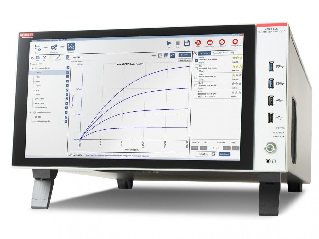
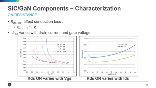
寬能隙半導體的 I-V 特性分析量測

I-V 特性分析
I-V 特性分析是一種基本方法,用以瞭解矽、碳化矽和氮化鎵基本特性中的電流與電壓關係比較。使用 SMU 或參數分析儀等儀器以及適當的軟體所產生的 I-V 圖形曲線,可用於顯示流經電子裝置或電路的電流與在其端子施加之電壓間的關係。最常見的 I-V 曲線組是系列曲線。
在寬功率封裝元件上進行測試
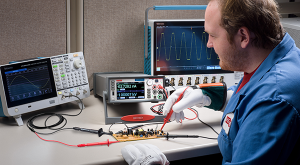
分析 SiC 或 GaN 晶圓和套裝零件位準裝置的電氣效能特性時,需要學習新技術,例如使用更高功率的儀器,處理探測和執行低位準量測的挑戰,(例如,在高崩潰電壓的情況下量測洩漏電流的皮安培位準。對於寬能隙半導體,更常見的是取得高達 3000 V 的電壓和高達 100 A 的電流。同樣重要的是最佳化測試系統,進而減少變更設定以進行開啟狀態、關閉狀態和電容量測所需的時間。

功率半導體裝置的崩潰測試
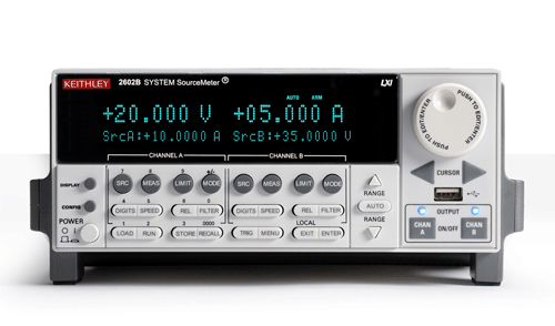
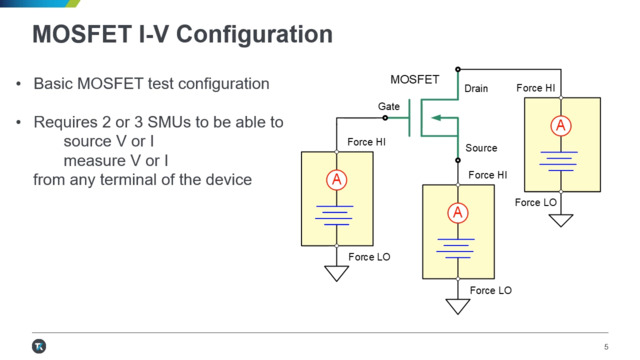
裝置的關閉狀態崩潰電壓決定了可套用到裝置的最大電壓。電源管理產品設計人員感興趣的主要耐受電壓是 MOSFET 的汲極和源極之間,或 IGBT 的集極和射極之間的崩潰電壓。對於 MOSFET 而言,閘極可以短路或強制進入「硬性」關閉狀態,例如對 n 型裝置施加負電壓,或將正電壓施加到 p 型裝置。這是一個非常簡單的測試,可使用一或兩個精密電源/量測設備 (SMU) 儀器進行。
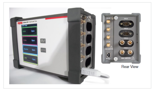
將儀器連接至探棒和測試治具
將高功率儀器連接到探測站和測試治具可能會是相當複雜的工作。不正確的連接通常會導致量測錯誤。8020 高功率介面面板可在 Keithley SMU 與各種半導體探測站或自訂測試治具之間提供高度精確、靈活且易於使用的介面。介面面板具有六個量測路徑,適用於 3 kV、200 V 和 100 A 的量測。您可以使用各種輸出接頭類型來配置五種路徑,以配合您的探測站。您可以使用選配的 T 型偏壓器配置四個路徑。這可在待測裝置的最多四個接腳上提供高電壓 C-V 量測。


進行高功率測試時安全第一
在寬能隙半導體上進行高功率測試時,安全性應始終是您的第一考量。為實驗室設計安全且合規的測試冶具絕非微不足道的小事。8010 高功率裝置測試治具提供安全、低雜訊、完整的環境,可測試各種高達 3000 V 和 100 A 的封裝裝置類型。可更換的插槽模組測試電路板可供用於多種封裝類型,包括使用者提供的插槽類型。
自動進行 I-V 特性分析的供電排序
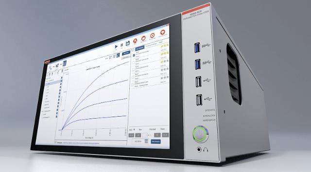
有了 Keithley 的自動化特性分析套件 (ACS) 軟體,就不用再費心進行程式設計。ACS 是一個彈性靈活的互動式軟體測試環境,針對裝置特性分析、參數測試、可靠度測試,甚至是簡單的功能測試所設計。ACS 支援各種 Keithley 儀器和系統、硬體組態及測試設定。藉由 ACS,使用者可用自動化硬體管理工具來設定其儀器,快速執行測試,而無須程式設計的知識。


-power-electronics-systems/fig-16.png?h=696&iar=0&w=1192)