Introduction
Full parametric characterization of a semiconductor device usually requires an array of tests to gather all of the device's important parameters. Current-voltage (I-V) tests are used to determine device parameters like transfer characteristics,leakages, and breakdown voltages. Capacitance-voltage (C-V) tests are used to determine device parameters like doping concentrations, interface charges, and threshold voltages. It is very common to perform both I-V and C-V tests on the same device, but the two test types require different test equipment and cabling. These differences make it difficult to perform I-V and C-V measurements on the same device quickly because changing test types typically requires recabling the entire system.
When configured with 4200-SMU, 4201-SMU, 4210-SMU,or 4211-SMU Source Measure Units (SMUs) and the 4210-CVU or 4215-CVU Capacitance Voltage Unit, the 4200A-SCS Parameter Analyzer is capable of performing both I-V and C-V measurements. However, the SMUs use triaxial cables and the CVU uses SMA coaxial cables. Combining the 4200A-SCS Parameter Analyzer with the 4200A-CVIV MultiSwitch eliminates these difficulties because the 4200A-CVIV is capable of switching between I-V and C-V measurements with no need to change cables or lift probe tips. The 4200A-CVIV is shown in Figure 1. The Clarius software that runs on the 4200A-SCS makes it simple to control the Multi-Switch and creates a faster, more efficient device testing workflow for any application that requires making I-V and C-V measurements on the same device.
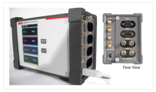
Note: Although this application note describes I-V and C-V switching with the 4200A-SCS, beginning with Clarius V1.4 or higher, each CVIV channel can be used as a bias tee by combining the CVU measurements with the SMU bias.With the bias tee capability, C-V measurements can be made at ±200 V or 400 V differential.
4200A-CVIV Operation
The 4200A-CVIV Multi-Switch is a four-channel multiplexed switching accessory for the 4200A-SCS that allows users to switch seamlessly between I-V and C-V measurements.It accepts four SMUs, one for each channel, and one CVU as inputs. Changing the output mode for each of the four channels reconfigures the internal switches of the 4200A-CVIV to route the desired signals to the output terminals. Figure 2 shows a simplified I-V and C-V switching diagram of the 4200A-CVIV.
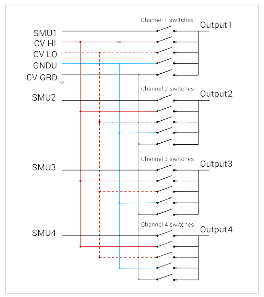
The 4200A-CVIV has six different output modes for each channel used for I-V and C-V switching. (There are additional output modes used for bias tee operation). The I-V and C-V switching output modes are described as follows:
- SMU - The SMU signal paths in the 4200A-CVIV are not multiplexed and cannot be switched between channels.Each SMU channel is directly associated with the channel to which it is connected. For example, setting Channel 3 to SMU will pass the signal from the SMU connected to Channel 3 to the output terminals for Channel 3.
- CV HI and CV LO - The CVU signal path in the 4200A-CVIV is fully multiplexed and can be assigned to any of the output channels. CV HI or CV LO can be assigned to any channel or any combination of channels to perform the desired C-V measurement. For example,setting Channel 1 to CV HI and Channels 2 and 3 to CV LO will configure the Multi-Switch to perform a C-V measurement on the device connected between Channel 1 and Channels 2/3.
- CV GUARD - This mode of the 4200A-CVIV can be used to remove undesired capacitances from C-V measurements. The CVU guard is the outside shield of the CVU coaxial cable. For example, setting Channel 4 to CV GUARD will configure the Multi-Switch to guard out capacitance from the device terminal connected to Channel 4.
- GNDU - The ground unit can be switched to any one of the four output channels. NOTE: Must have 4200A-CVIV Hardware Version 2.0 or higher and Clarius V1.4 or higher.
- OPEN - Configuring any channel to OPEN will open all of the output relays connected to that channel.
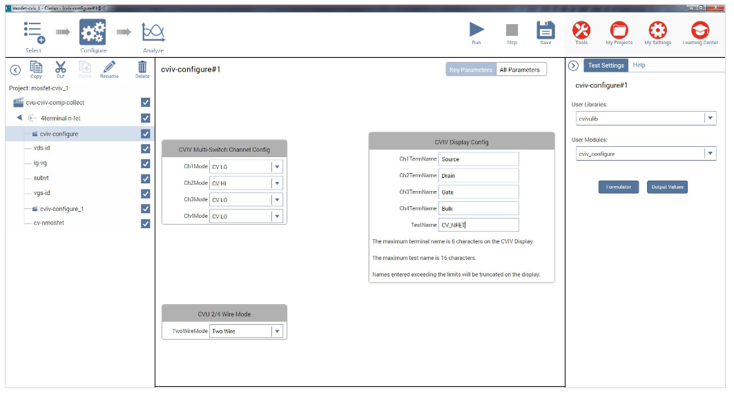
The 4200A-CVIV is controlled using the Clarius software application that comes with the 4200A-SCS Parameter Analyzer. Switch configurations are controlled by placing the cviv-configure Action from the Action Library into the project tree.
The cviv-configure Action is used to switch the channel output configuration, two-wire/four-wire CVU setting, and the names of the test and channels to be shown on the 4200A-CVIV display. A cviv-configure Action must be used any time the configuration of the 4200A-CVIV needs change. Figure 3 shows an example of the cviv-configure Action populated with settings to switch the CVU output terminals to a MOSFET.
The cvu-cviv-comp-collect Action performs CVU connection compensation through a 4200A-CVIV on a user-defined configuration. Open, Short, and Load correction compensations can be acquired. Connection compensation corrects for offset and gain errors caused by the connections between the CVU and the device under test.The compensation for each particular switch configuration is automatically stored so that when a particular configuration is recalled using the cviv-configure Action, the compensation will automatically be applied if it is enabled within a C-V measurement test. Figure 4 shows the cvu-cviv-compcollect Action setup to perform an Open compensation.

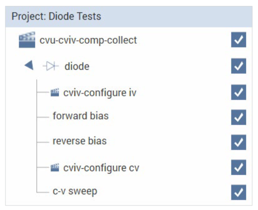
Figure 5 shows a screen capture of a project called Diode Tests that is used to make I-V and C-V measurements on a diode that is connected to the outputs of Channels 1 and 2. First, compensation is performed using the cvu-cviv-comp-collect Action. Then the cviv-configure-iv Action connects SMU1 and SMU2 to Channels 1 and 2 so that the forward and reverse I-V measurements can be made in the two tests that follow. When the cviv-configure-cv Action is executed, the SMUs are disconnected from the outputs and the CVU HI and LO terminals are connected to Channels 1 and 2. Finally, a C-V sweep is made on the diode.
C-V/I-V Switching for Device Characterization
Both I-V and C-V measurements play a role in the parametric characterization of semiconductor devices. Two-terminal devices require simple I-V sweeps to characterize their DC performance and C-V sweeps to determine the capacitance between their two terminals at different bias levels. For example, full characterization of a diode requires I-V measurements to acquire the forward I-V curve, reverse leakage curve, and reverse breakdown voltage. C-V measurements are used to acquire the diode's doping profile and charge density information.
Two-terminal Devices
Two channels of the 4200A-CVIV are used to connect to the diode for I-V and C-V measurements. Since diodes have very low impedance forward active characteristics, it's best practice to perform measurements in four-wire mode to prevent measurement inaccuracies due to losses in cabling.Four-wire mode, also called remote sense, forces a test current through one set of cables and measures a voltage directly at the device under test with another set of cables.This technique helps remove the effects of cable impedance from the measurements.
Figure 6 shows the device connections and 4200A-CVIV settings for an I-V test on a diode. All of the DC I-V characteristics of the diode are collected in this configuration.The connections to the diode are made with triaxial cables, Model 4200-TRX-.75 (75cm or approximately 30 inches).These shielded cables are used to ensure that both very low current I-V measurements and high frequency AC measurements can be made with high accuracy. The device can be a packaged part in a test fixture or located directly on a wafer in a probe station.
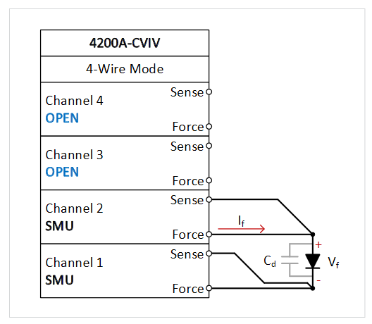
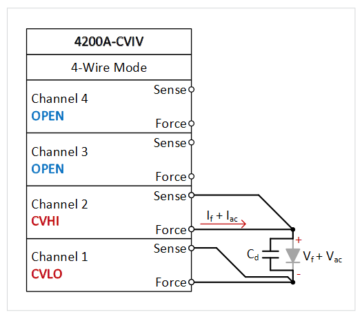
The gray capacitor in Figure 6 (Cd) is the parasitic capacitance of the PN junction. The I-V test does not provide information about this parasitic capacitance. A C-V test is necessary to characterize the capacitance of the device.Figure 7 shows the device connections and 4200A-CVIV settings for a C-V test on a diode. All of the connections are identical to the I-V test. When the cviv-configure Action is executed in the Clarius software, the output is switched from the SMUs to the CVU terminals.
Three-terminal Devices
Three-terminal devices require more complicated I-V characterization and often capacitance measurements between multiple combinations of terminals. For example,bipolar junction transistors (BJTs) are three-terminal devices that require multiple SMUs to measure their transfer characteristics and produce useful data, such as Gummel plots. The 4200A-CVIV, when coupled with three SMUs and one CVU in the 4200A-SCS, can make these measurements.
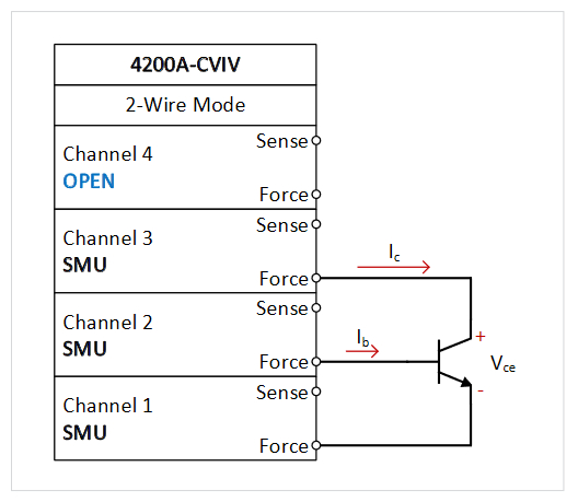
Figure 8 shows the device connections, and 4200A-CVIV settings, for an I-V test on a BJT. The configuration is shown in two-wire mode, also known as local sense, but remote sensing should be used for high current BJTs. All of the connections to the BJT are made with the 4200-TRX-.75 triaxial cables. The device can be a packaged part in a test fixture or located directly on a wafer in a probe station.
Once the I-V measurements are complete, the 4200A-CVIV can be seamlessly switched to measure the parasitic capacitances of the BJT junctions without changing cables or removing connections to the device. Figure 9 shows the parasitic capacitances between the BJT’s terminals to be measured.
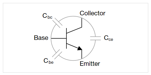
To measure the capacitance between two terminals, it is necessary to guard the third terminal to remove the effects of the additional parasitic capacitors. F or example, to measure the base-emitter capacitance (Cbe,), the collector is connected to guard. The 4200A-CVIV provides this guard signal with the CV GUARD setting. Figure 10 shows the cviv-configure settings that instruct the 4200A-CVIV to use the CV GUARD signal. In this example, the CV HI terminal is connected to base (b) through Channel 2, CV LO is connected to the emitter (e) through Channel 1, and CV GUARD is connected to the collector (c) through Channel 3.
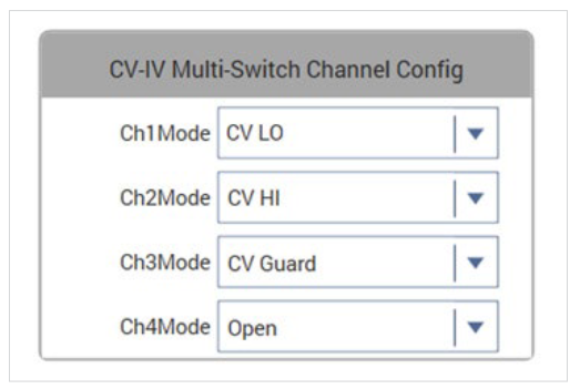
Figure 11 shows the device connections, and 4200A-CVIV settings, for a guarded capacitance measurement on the Cbe of a BJT.
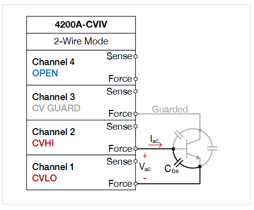
The same technique is used to measure the base-collector capacitance or the collector-emitter capacitance of the BJT.The 4200A-CVIV can be controlled by the Clarius software to make all of these measurements automatically without moving cables between the terminals. The Clarius software includes a project (cvu-bjt-cviv) that is configured to measure these three parasitic capacitances present in a BJT using the CVU and the 4200A-CVIV to switch the CVU between terminals of the device.
Four-terminal Devices
Four-terminal devices, such as a MOSFET with a separate bulk connection, have more terminal-to-terminal parasitic capacitances, and more potential I-V and C-V measurement combinations than lower terminal count components. The 4200A-CVIV, when fully configured with four SMUs and one CVU, addresses these measurements with flexible configurability.
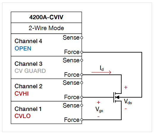
Figure 12 shows the device connections, and 4200A-CVIV settings, for an I-V test on a four-terminal MOSFET. The configuration is shown in two-wire mode, also known as local sense, but remote sensing should be used for high current MOSFETs. All of the connections to the MOSFET are made with 4200-TRX-.75 triaxial cables. The device can be a packaged part in a test fixture or located directly on a wafer in a probe station.
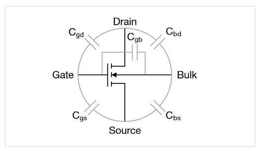
Capacitance measurements are often made on MOSFETs to explore their basic operation and various parameters.Given that the high frequency operation and switching speeds of a MOSFET are dependent on the capacitance of he device, capacitance measurements are often made on various parasitic capacitances of the device, as shown in Figure 13. For example, the capacitance between the gate and channel (Cgd and Cgs) is important because it creates the charges necessary for operating the devices. This gatechannel capacitance depends on the applied voltage and the operating region.
The C-V characteristics of the capacitor formed between the gate and the source, drain, and bulk of the MOSFET structure can be used to determine characteristics of the MOSFET like the threshold voltage, oxide thickness, oxide capacitance,and doping density. Figure 14 shows the most common way of configuring this measurement. The source, drain, and bulk terminals are physically tied together and a C-V sweep is performed between the gate and the other three terminals.
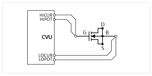
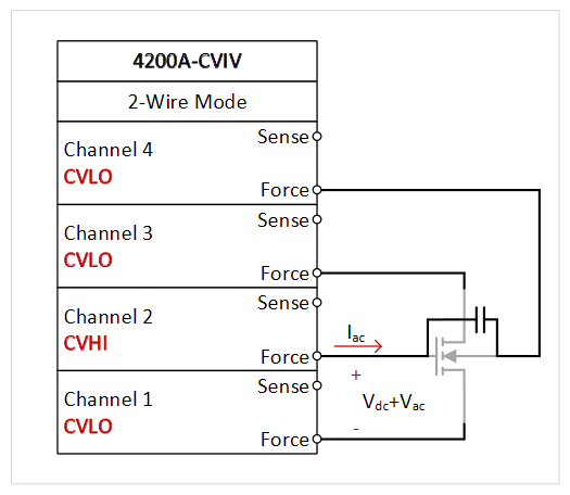
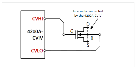
The CVHI, CVLO, and CV GUARD signals of the 4200A-CVIV can each be assigned to more than one pin at a time. This removes the need to tie the source, drain, and bulk together physically at the device to perform this measurement;instead, the connections are made internal to the 4200A-CVIV. Figure 15 shows the device connections, and 4200A-CVIV settings, for this C-V test on a four-terminal MOSFET. Channels 1, 3, and 4 are all assigned to CVLO in this configuration. Figure 16 shows the equivalent circuit of this 4200A-CVIV configuration.
Conclusion
The 4200A-CVIV Multi-Switch makes it easy to perform I-V and C-V measurements on the same device without the need to change cables, which could potentially introduce errors or damage devices. The 4200A-SCS and Clarius software make it simple to control the 4200A-CVIV and integrate C-V and I-V testing together into a single project that executes seamlessly and continuously.
Find more valuable resources at TEK.COM
Copyright © Tektronix. All rights reserved. Tektronix products are covered by U.S. and foreign patents, issu ed and pending. Information in this publication supersedes that in all previously published material. Specification and price change privileges reserved. TEKTRONIX and TEK are registered trademarks of Tektronix, Inc. All other trade names referenced are the service marks, trademarks or registered trademarks of their respective companies.
040320 1KW-60635-0

