Introduction
The power electronics market, driven by new wide bandgap (WBG) semiconductor devices is expected to grow by a 4.3% compounded annual growth rate (CAGR) through 2025 to a level around $22B. Power transistors are expected to be the largest and fastest growing segment of the discrete semiconductor industry, with much of this growth being driven by new energy efficiency-related applications and technologies for electric vehicles (EV), hybrid electric vehicles (HEV), energy storage applications, and even for upcoming Urban Air Mobility (UAM systems).
Many segments of the electronics industry, including the semiconductor industry, are focused on efficiency of energy generation, transmission, and consumption. Device manufacturers have traditionally relied on silicon (Si) technology for creating many of the devices used to control motors, regulate voltages, convert power, etc. Given that most power semiconductor devices are used as switches or blocking devices in these applications, this translates into creating devices that offer lower leakage, lower ON resistance, or both.
Wide-bandgap semiconductors including gallium nitride (GaN) and silicon carbide (SiC) are exceeding the capabilities of Si. Electrically, these substances are closer to insulators than silicon and other typical semiconductor materials. Their adoption is an effort to overcome limitations of silicon that stem from it being a narrow bandgap material, which leads to undesirable conductive leakages that become more pronounced with increases in temperature, voltage, or frequency
Why GaN and SiC?
These newer materials typically have much higher power density, smaller size, better high temperature performance, higher frequency response, lower leakage, and lower ON resistance than silicon, all of which add up to greater operating efficiency. Of the two wide-bandgap materials, GaN is suited primarily to low- to mid-range power implementations, under approximately one kilovolt and 100 amps. A notable area of growth for GaN is its use in LED lighting, and usage is growing for additional low-power usages such as electronics power supplies and RF power amplifiers. By contrast, the technologies surrounding SiC are both better developed than GaN and better suited to higher power implementations such as power transmission, largescale HVAC equipment, and industrial systems.
SiC-based metal-oxide-semiconductor field-effect transistors (MOSFETs) offer significant advances over earlier Si devices for use in power modules, as represented in Figure 1.
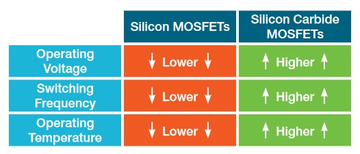
Compared to Si MOSFETs, SiC devices are capable of operating at higher voltages, higher switching frequencies, and higher temperatures. Under these conditions, SiC provides higher performance, efficiency, power density, and reliability. This combination of benefits is helping designers reduce the size, weight, and cost of power converters, making them more competitive especially in lucrative market segments such as aerospace, military, and electric vehicles.
Comprehensive Testing Across the Device Lifecycle
Bench testing plays an important role at every stage of the development of power electronics and conversion modules to characterize, benchmark, and document efficiency and other characteristics. It begins with testing the material to determine whether it is suitable for use, followed by additional testing after the wafer has been fabricated but before circuits are lithographed onto it. Testing proceeds on the manufactured component, then in an assembled circuit, and finally on the piece of power conversion component when it comes off the assembly line.
Each of these testing phases has individual importance to the undertaking as a whole, and each must be conducted at a specific point during the production process. For example, breakdown voltage testing must be done on a MOSFET as a stand-alone component, before it is installed on a circuit board. Likewise, switching energy must be measured after the MOSFET is installed on a circuit board, because that energy depends on factors associated with the circuit as a whole, with switching frequency depending on the gate driver, for example.
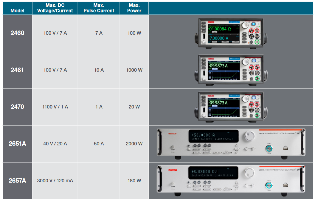
Tektronix and Keithley provide a comprehensive set of Source Measure Units (SMU) with various high voltage and high current ranges that gives design and test engineers the ability to set up test benches robust enough to meet their most rigorous requirements (Table 1). This equipment also sets the stage for emerging requirements that will come to the forefront as power-conversion equipment becomes more sophisticated, the regulatory environment becomes more rigorous, and testing protocols become more challenging.
What are Source Measure Units (SMU)?
Essentially, SMUs are fast-response, read-back voltage and current sources with high accuracy measurement capabilities, all tightly integrated in a single enclosure. SMUs combine the capabilities of a semiconductor parametric analyzer, precision power supply, true current source, DMM, low-frequency ARB, pulse generator, electronic load, and trigger controller – all in one full-rack, four-quadrant instrument. With early SMUs that were available in the early 1990's, the major shortcoming of these instruments was their limited range – existing SMUs simply couldn't deliver the power levels required to characterize high power semi devices accurately. Keithley addressed the power level requirements with the above instruments starting back in 2011 with the launch of the 2651A High Power System SourceMeter® SMU to the most recent launch of the 2470 High Voltage SourceMeter SMU in 2019.
Critical high power semiconductor transistor testing
For SiC and GaN testing, there are a number of common static device parameters tests that are performed including:
- I-V Characteristics, including family of curves and leakage current.
- On-Resistance, Off Resistance
- Breakdown Voltage, Leakage Current Test
These parameters can be divided into two broad categories: those that determine the performance of the device in its ON state and those that determine the performance in its OFF state. The instruments listed in Table 1 are support these tests. These tests will now be discussed.
ON-State Characterization
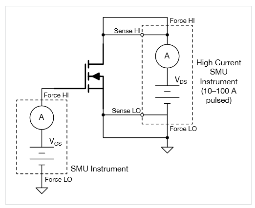
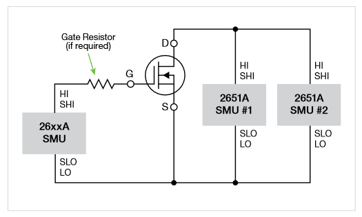
ON-state characterization is typically performed using a high current instrument like the 2460, 2461, and 2651A, capable of sourcing and measuring low-level voltages. If the device has three terminals, then a second SMU instrument is used at the device control terminal to place the device in the ON state. For a typical configuration for characterizing the ON-state parameters of a power MOSFET, see Figure 2.
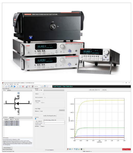
Figure 3 illustrates a typical high power SMU system and Keithley's ACS-BASIC software to perform the tests composed of high voltage and high current SMUs.
Use 8010_2675A_2651A_2612A.tif available from the Widen portal. Use the "acs_be_screesnhot.tif"(https://tektronix.widencollective.com/dam/assetdetails/asset:65b2569e-5287-40cc-bc09-5ee055f7573d/false?inav=false)
Let's examine the configuration details and measurement challenges of a few ON-state parameters.
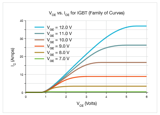
One of the most readily recognizable set of test results for a semiconductor device is a plot of its output characteristics. Output characteristics are normally shown in graphical form on the device's data sheet and depict the relationship between the output voltage and current. For a gated power semiconductor switch, such as a MOSFET or IGBT, output characteristics are commonly referred to as the "family of curves." Figure 4 shows the family of curves for a IGBT type power transistor.
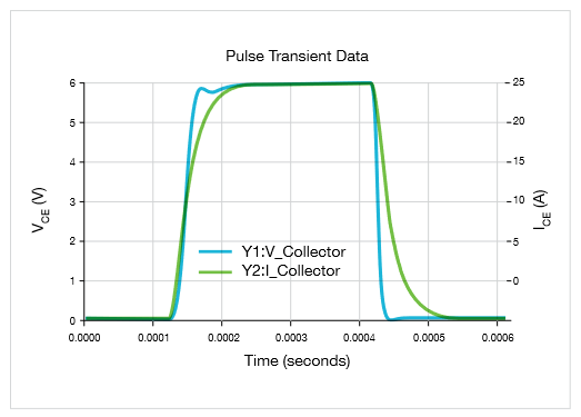
Pulsed testing is common in power semiconductor test because DC testing can cause the device to self-heat, which can alter the measured characteristics. Implementing a pulsed test with multiple SMU instruments requires precise control of the timing of source adjustments and measurements and is often coordinated by means of a computer program. For consistent results, it is important to validate the system. This can be done by sourcing a single pulse through the system and measuring the response at the device. Capturing the complete pulse waveform as a function of time allows selecting appropriate source and measure delays so that the device turns on properly and measurements are made after the system is settled. The high speed A/D converters in the Series 265xA High Power System SourceMeter® SMUs and the 2460 High Current SourceMeter SMU instruments are useful for monitoring the voltages and currents at the device as they relate to time. Figure 5 depicts the results of a pulse transient characterization of voltage and current vs. time.
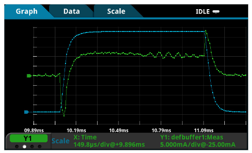
Using the 2461's built-in graphing capabilities, you can view similar pulse I-V responses right on the front panel as shown in Figure 6.
On-state voltage
The semiconductor device's ON-state voltage directly impacts the conduction loss. Power consumed by or lost in the device is equal to the product of the ON-state voltage and the load current. This power is not delivered to the device. Typically, device manufacturers want to characterize how the ON-state voltage and, by extension, the conduction loss, varies with temperature and load current. Keithley's high current SMU instruments are commonly used in these characterizations.
To measure the ON-state voltage, the high current SMU instrument is configured to output current to the device and measure voltage. For 3-terminal SiC or GaN devices, a second, lower-power SMU instrument is used at the gate terminal to place the device in the ON state. Because power semiconductors are typically high current devices, ON-state voltage is generally measured using a pulsed stimulus to avoid any change in device parameters as a result of device self-heating due to a DC test current.
Two key elements help ensure a successful ON-state voltage test: (1) accurate voltage measurement and (2) proper cabling and connections. Accurate voltage measurements are crucial because ON-state voltage varies with temperature. For instance, a few millivolts of difference in the forward voltage of a power diode can indicate a change of several degrees in the temperature at the device. High speed A/D converters in the Keithley 2651A and 2461 enable the engineer to make very accurate voltage measurements at 1 μs intervals with pulse widths as short as 100 μs.
Proper cabling and connections are equally key to minimizing voltage errors. During the application of high currents to power devices, ON-state voltages of 1–3 V are very common. During testing, such high currents can generate voltage drops across test leads and test lead connections between the instrument and the DUT. These additional voltages create errors in the voltage measurement. Four-wire or Kelvin connections eliminate most of these voltage errors from the measurement by using separate Sense test leads for the SMU. Minimal current flows in these leads, creating virtually no voltage drops between the instrument and DUT, so the instrument measures the voltage seen at the DUT.

The use of low inductance cables helps ensure good pulse fidelity (i.e., short rise and fall times) when testing high current devices, which provides more time for measurement within a given pulse width. The 2651A SMU Instrument comes with a specialized low resistance, low inductance cable assembly appropriate for generating 100 μs pulses at 50 A.
Transfer characteristics
A device's transfer characteristics allow evaluating its transconductance and therefore its current carrying capability. Transfer characteristics have an indirect relationship to determining switching time and estimating switching losses. The transfer characteristics are often monitored vs. temperature in order to gauge temperature's effect on the device's maximum current handling capability. Two SMU instruments are required for measuring the transfer characteristics: one sweeps the input voltage on the control terminal of the device and the second biases the output terminal and measures the output current. Typical transfer characteristic measurements include the gate voltage vs. drain current plot for a MOSFET (VDS–ID), the gate voltage vs. collector current plot for an IGBT (VGE–IC), and the Gummel plot for a BJT (VBE vs. IC, IB). In some cases, a wide range of output current is measured. This is especially true for the Gummel plot of a BJT, where several orders of magnitude of current are traversed. In these cases, the 2651A is very useful because it can measure currents from the nanoamp range up to 50 A.
ON-resistance
The figure of merit for a power MOSFET is the product of ONresistance (RDS(on)) and gate charge (QG). The ON-resistance is the key determinant of the conduction loss of the power MOSFET. The conduction loss is equal to I2 D * RDS(on). Newer devices have ON-resistances in the range of a few milliohms to tens of milliohms at high current. This requires very sensitive voltage measurement capability at the drain terminal. Measuring ON-resistance requires the use of two SMU instruments: one SMU instrument drives the gate into the ON state and a second SMU instrument pulses a defined current at the drain and measures the resulting voltage. The ON-resistance is calculated using Ohm's Law and the programmed drain current and measured drain voltage.
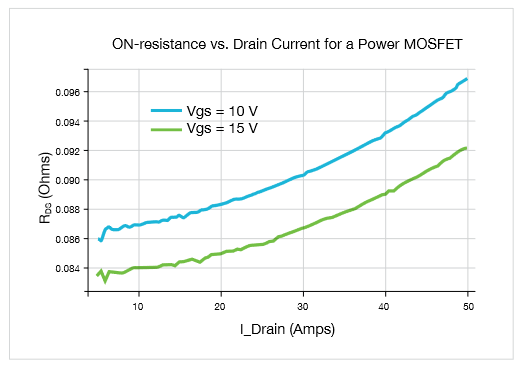
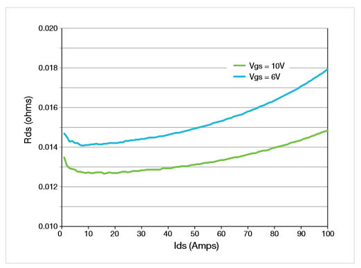
ON-resistance is often characterized as a function of drain current or gate voltage. Using software, both SMU instruments can be triggered and swept so that this measurement is performed within a single test. Figure 8 shows an example of a calculated set of RDS(on)vs. drain current results at two different gate-source voltage levels.
For very high current devices, two 2651A SMUs can be used in parallel to generate current pulses up to 100 A. When two 2651As are connected in parallel with Keithley's TSP-Link® technology, the current range is expanded from 50 A to 100 A. When two units are connected in series, the voltage range is expanded from 40 V to 80 V. The built-in intelligencesimplifies testing by enabling the units to be addressed as a single instrument, thus creating an industry-best dynamic range (100 A to 1 pA). This capability enables you to test a much wider range of power semiconductors and other devices. Let's go through a bit of theory to confirm this.
Figure 9 illustrates connecting two 2651A SMUs in parallel to achieve a 100 A current pulse. Figure 10 shows an example Rds(on) measurement data on a power MOSFET device using two 2651As connected in parallel.
To learn more about connecting two 2651A's in parallel to output up to 100 A current pulse, we suggest reading the Tektronix/Keithley Application Brief "Testing to 100 A by Combining Keithley 2651A High Power SourceMeter® Instruments".
ON-resistance increases with breakdown voltage, so any process adjustments made to increase the breakdown voltage will involve later testing of ON-resistance in order to assess the overall impact of process changes. Obtaining more efficient devices at higher voltages is one of the drivers for further research on SiC and GaN devices, which offer ON-resistances smaller than silicon devices' at high withstand voltages.
OFF-State Characterization
To gain an adequate understanding of overall product efficiency, the impact of the device on the overall circuit when the device is turned off must be investigated. For high power devices, OFF-state characterization often involves the use of a high voltage instrument capable of sourcing hundreds or thousands of volts and measuring small currents. OFF-state characterization is often performed between two device terminals (regardless of the total number of device terminals), so a single SMU instrument is often sufficient to perform the measurement. However, an additional SMU instrument can be used to force the device into its OFF state or to add certain stress to certain terminals.
Keithley SourceMeter SMU instruments cover a wide range of voltages and currents for characterizing the OFF state of power semiconductor devices. The 2657A can source up to 3 kV and measure currents with 1 fA resolution. The 2470 can source 1100 V and measure currents with 10 fA resolution.
Two primary DC tests are performed when the device is off:breakdown voltages and leakage currents. Let's consider these individually.
Breakdown voltages
A device's OFF-state breakdown voltage determines the maximum voltage that can be applied to it. The primary withstand voltage of interest to power management product designers is the breakdown voltage between drain and source of a MOSFET or between the collector and emitter of an IGBT. For a MOSFET, the gate can be either shorted or forced into a "hard" OFF state, such as by applying a negative voltage to an n-type device or a positive voltage to a p-type device. This is a very simple test that can be performed using one or two SMU instruments. The lower power SMU instrument is connected to the gate and forces the transistor off. It can force 0 V for a gate shorted test or force a user-specified bias voltage. A high voltage SMU instrument, such as the 2657A or 2470, forces current into the drain and measures the resulting drain voltage.
Most MOSFETs typically have breakdown voltages higher than the value specified on the data sheet. Therefore, it is useful to define the voltage limit of the drain SMU instrument to a value higher than the specified breakdown voltage. Additionally, as the drain terminal is driven closer and closer toward avalanche, the behavior of the currents and voltages of the device under test (DUT) may begin to change.
Another way of characterizing breakdown voltages involves forcing a voltage across the terminals of interest (e.g., drain and source of a MOSFET) and measuring the resulting current. The breakdown voltage is defined as the voltage at which the current exceeds a specified threshold, for example, 1 mA. Limit the maximum current in order to prevent destruction of the device during testing. Keithley SourceMeter SMU instruments include built-in programmable features to limit the maximum voltage and current to the device precisely and quickly. As with any protection device, the limit control of the SMU instrument has a finite response time. Some devices may have extremely fast and hard breakdown behavior in which the device impedance changes by several orders of magnitude in a very short period. When the device breaks down faster than the SMU instrument can respond, use series resistors to limit the total maximum current through the device.
Since you will be working with very high voltages, safety must be one of the first considerations for high voltage characterization of power semiconductor devices. Keep in mind the voltage ratings for all terminals, connectors, and cables. For example, Keithley SourceMeter SMU instruments are electrically floating, which means that measurement common is not tied to protective earth (safety ground). Unless the user ties measurement common to safety ground, then he must take high voltage precautions at all terminals if the SMU instrument can generate more than 42 V.
When configuring a test system, it's important to protect the operator from electric shock. One primary way to do this is to use a safe test enclosure that surrounds the DUT and any exposed connections. Pairing a safe enclosure with a safety interlock also minimizes risk of electric shock when the user changes test connections. The Keithley SMUs listed in Table 1 equipped with a safety interlock; when properly installed, this interlock ensures that the hazardous voltages are disconnected whenever a user opens the test fixture or accesses the wafer in a probe station.
If you are testing devices and circuits on a bench, there is a risk you could come in contact with energized circuits, creating a safety hazard. Always use the proper safety gloves when working with high voltages on energized components as shown in Figure 11.

Leakage currents
Leakage current is the level of current that flows through two terminals of a device even when the device is off. It factors into the standby current of the end product. In most cases, temperature and the voltage across the terminals of interest will affect leakage current. Minimizing leakage current minimizes power loss when the device is off. This power is consumed by the device and is not output to the load and therefore contributes to power inefficiency. When using a transistor or diode to switch or rectify, it's important to make a clear distinction between ON and OFF states; therefore, a lower leakage current means having a better switch.
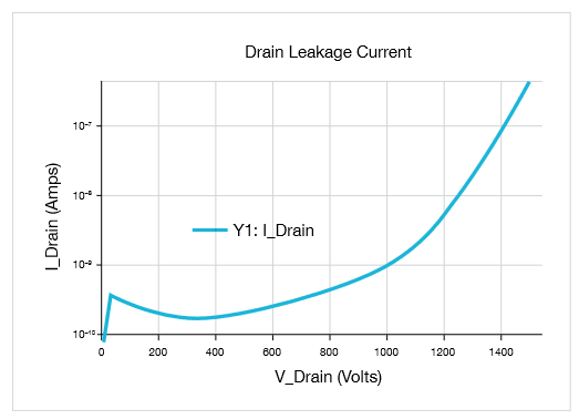
While testing a device's OFF state, it is generally desirable to test the gate leakage current and drain or collector leakage current. For power devices, these values are typically within the nanoamp and microamp ranges, so they can be measured using the sensitive current measurement capability of Keithley SMU instruments. This capability can be greatly beneficial when testing devices made of wide bandgap materials such as silicon carbide, gallium nitride, and aluminum nitride, which typically have higher breakdown voltages and lower leakage currents than do silicon devices. Figure 12 is a plot of OFF-state drain voltage vs. drain current results for a commercially available SiC power MOSFET.
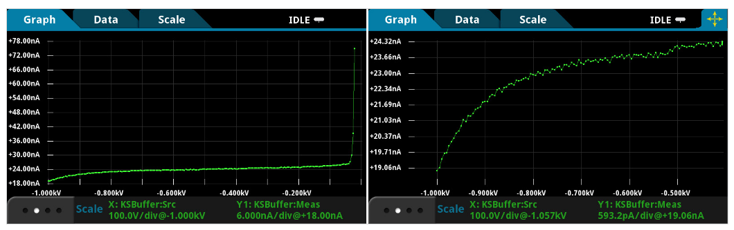
The 2470's graphical plotting view can give you immediate leakage current results right on the front panel as shown in Figure 13. The 2470 also provides oscilloscope like cursors so you can analyze the data right on the front panel.
Triaxial cables are essential to achieving accurate low current measurements in part because they permit carrying the guard terminal. Guarding eliminates the effect of system leakage currents by routing them away from the measurement terminal. Additionally, guarding reduces settling time in high voltage applications by virtually eliminating the need to charge the cable capacitance. Using a guarded test fixture or prober allows the benefits of guarding to be extended to the DUT. Keithley offers triaxial cables and connections for all its SMU instruments that are tailored for low current measurements, such as the 2470 and 2657A.
Electrostatic shielding is another important consideration for low current measurements. An electrostatic shield is a metal enclosure that surrounds the circuit and any exposed connections. The shield is connected to measurement common to shunt electrostatic charges away from the measurement node.
Finally, system validation is important for low current characterization to ensure that the measurement is settled. Settling time increases as the expected current decreases. Keithley's high power SMU instruments have auto delay settings that set reasonable delays to achieve good measurements while taking the instrument's settling characteristics into account. However, to account for any unguarded system capacitance, perform a measurement validation by stepping voltage and measuring the resulting current through the system. Use the results from the validation to set additional source and measure delays in order to achieve consistent measurements.
Conclusion
Wide bandgap materials are overcoming limitations of their silicon predecessors for the development of power MOSFETs. The ability to operate at higher voltages, frequencies, and temperatures than silicon set the stage for the next generation of power modules, by delivering a breakthrough combination of cost and energy efficiency. Design and production of semiconductors and power modules based on SiC demand more rigorous testing than with previous generations.
Coupling any of Keithley's high power SourceMeter SMU instruments meet all these needs and further facilitates research of high voltage materials and semiconductor devices. Additionally, Keithley has the appropriate cabling accessories and test fixtures that allow safe, accurate, and reliable testing which can cost-effectively meet rigorous design requirements. Being prepared to certify devices against regulatory changes and the needs of new technologies from power generation to end user devices such as electric vehicles enable companies that make power electronics to focus on the value-added innovation that defines the future.
Find more valuable resources at TEK.COM
Copyright © Tektronix. All rights reserved. Tektronix products are covered by U.S. and foreign patents, issued and pending. Information in this publication supersedes that in all previously published material. Specification and price change privileges reserved. TEKTRONIX and TEK are registered trademarks of Tektronix, Inc. All other trade names referenced are the service marks, trademarks or registered trademarks of their respective companies.
091021 1KW-73841-0