Introduction
Devices such as Power MOSFETs (metal-oxidesemiconductor field-effect transistors) and IGBTs (insulated-gate bipolar transistors) are used in a wide variety of applications. Power MOSFETs are the most widely used power device worldwide and are often utilized as highspeed switching devices for applications such as control modules in automotive electronics. IGBTs are the next most widely used power device for switching and amplification applications, second only to Power MOSFETs.
Both MOSFETs and IGBTs are three terminal devices used in switching and signal amplification. A MOSFET's terminals include the source (S), gate (G), drain (D) and occasionally the body as a fourth terminal when its not connected to the source. The terminals of an IGBT are the emitter (E), gate (G), and collector (C). Despite the similarities in their usage, MOSFETs and IGBTs operate differently. For example, IGBTs can handle very high voltage and power, while MOSFETs are better for very high frequency applications. As a result, the turn off time and switching speed of a MOSFET is quicker, but an IGBT produces lower forward voltage drop and can accommodate transient voltage and current.
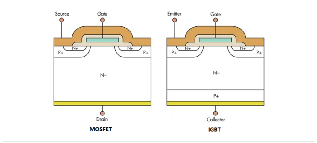
Much of this application note will reference MOSFETs, but most of the content therein also applies to IGBTs. Simply swap "drain" with "collector" and "source" with "emitter."
The switching speed of the device is affected by internal capacitances and are typically specified in data sheets, but the gate charges (Qgs and Qgd) can also be used to assess the switching performance of a MOSFET or IGBT.
One method of measuring the gate charge of a MOSFET is by forcing a gate current while the gate to source voltage is measured as a function of time. From the resulting gate voltage waveform, the gate-source charge (Qgs), gate-drain charge (Qgd), and gate charge (Qg) are obtained.
The Keithley Automated Characterization Suite (ACS) software supports making gate charge measurements on MOSFETs using two source measure unit (SMU) instruments and the gateCharge.py Python Test Module (PTM) that is included with the software. This test is one of many included in the extensive test libraries provided in the ACS Software Suite.
Gate Charge Measurements
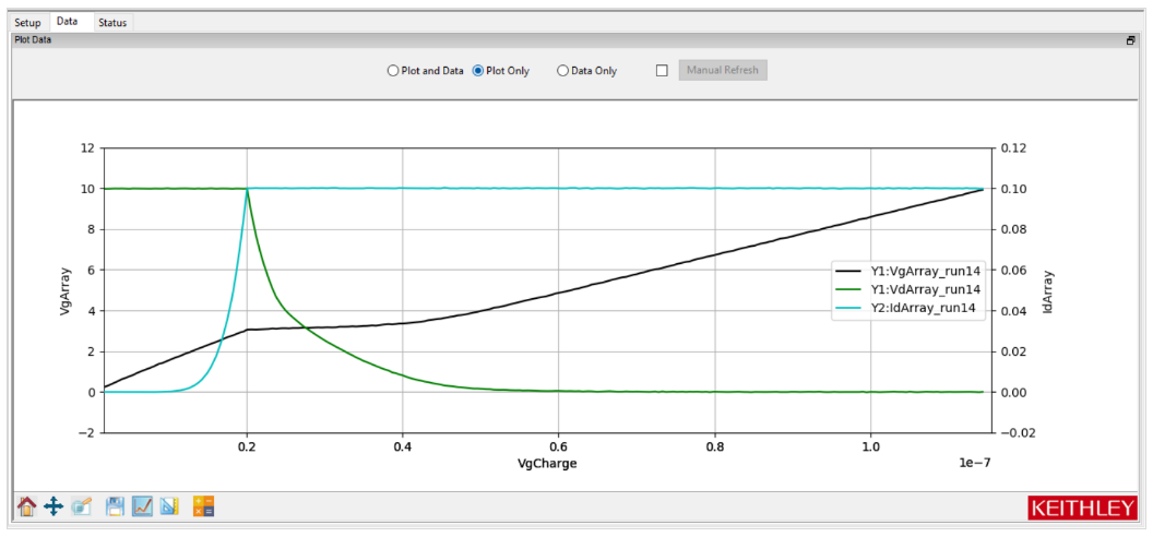
In the Gate Charge Method, a fixed test current (Ig) is forced into the gate of a MOS transistor and the measured gate source voltage (Vgs) is plotted against the charge flowing into the gate. A fixed voltage bias is applied to the drain terminal. Figure 2 shows the gate voltage vs. gate charge of a power MOSFET.
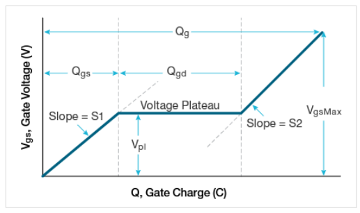
The gate charge (Q) is derived from the forced gate current and time, (Igdt). The gate-source charge (Qgs) is the charge required, as shown in Figure 2, to reach the beginning of the plateau region where the voltage (Vgs) is almost constant. The plateau (or Miller) voltage (Vpl) is defined, according to the JEDEC standard, as the gate-source voltage when dVgs/dt is at a minimum. The voltage plateau is the region when the transistor is switching from the OFF state to the ON state. The gate charge required to complete this switching, that is the charge needed to switch the device from the beginning of the plateau region to the end, is defined as gate-drain charge (Qgd) and is known as the Miller charge. The gate charge (Qg) is the charge from the origin to the point where the gate-source voltage (Vgs) is equal to a specified maximum (VgsMax).
S1 is the slope of the line segment from the origin to the first plateau point. S2 is the slope of the line segment from the last plateau point to the specified maximum gate voltage (VgsMax). The slopes are used to calculate Qgs and Qgd, as specified in the JESD24-2 standard.
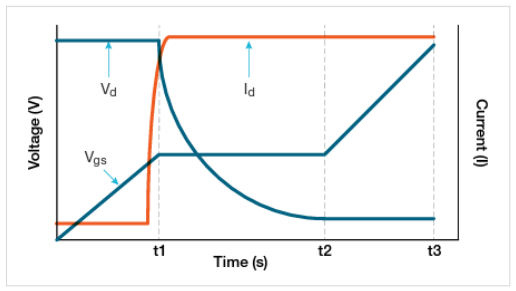
Figure 3 shows typical gate and drain waveforms as a function of time. As current is forced to the gate, Vgs increases until it reaches the threshold voltage. At this point, the drain current (Id) begins to flow. When Cgs is charged up at time t1, Id stays constant and the drain voltage (Vd) decreases. Vgs remains constant until it reaches the end of the plateau. Once Cgd is charged at time t2, the gatesource voltage (Vgs) starts to increase again until it reaches the specified maximum gate voltage (VgsMax).
Gate Charge Measurement Test Setup
Two SMUs are used to measure gate charge with ACS software. Figure 4 illustrates a basic circuit diagram of the gate charge test. SMU1 is connected to the gate terminal of the MOSFET and forces the gate current (Ig) while measuring the gate-source voltage (Vgs) as a function of time. Meanwhile, SMU2 applies a fixed voltage (Vds) to the drain at a specified current compliance (Ids).
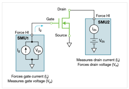
While the test is running, the gate voltage increases and causes the MOSFET to enter its ON state. During this transition, the drain SMU (SMU2) switches from voltage control to the current control mode, because the current exceeds the specified compliance level. The software returns the measured drain current transients and drain voltage during the transition from the OFF state to the ON state.
The MOSFET's source terminal is connected to the Force LO terminal or ground.
ACS Software Configuration
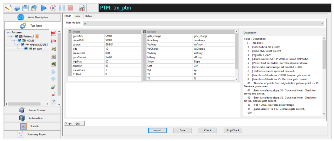
The Gate Charge test can be accessed by adding a device to the project tree, selecting it, and clicking "New PTM." From there, click the import button and select "gateCharge.py" from the PTM Library using the file explorer. This will add the gate charge test to the project tree below the device under test.
The gate charge PTM is compatible with 26xx Series SMUs and S4200 SMUs.
Input Parameters
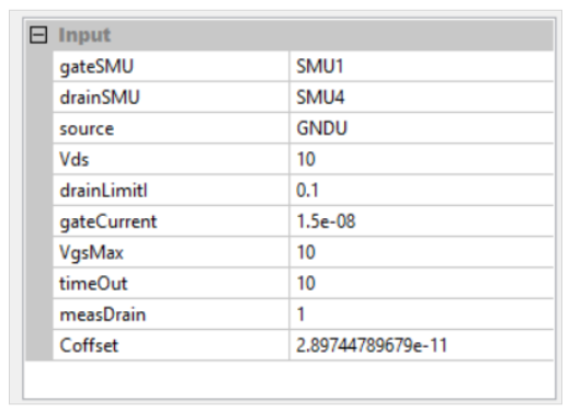
Before test execution, the input test parameters are entered in the Input table in the Setup tab. The ideal input parameters will vary depending on the device and which model of SMU is used.
Descriptions of the input parameters are listed in Table 1. First, enter the SMU numbers that are connected to the gate (gateSMU) and drain (drainSMU) of the MOSFET. The source terminal should always be connected to the GNDU, or Force LO.
The magnitude of the current forced to the gate by the gateSMU, is the gateCurrent (Ig) parameter. The drain voltage (Vds) is the bias voltage applied to the drain and drainLimitI is the compliance current (Ids) of the drain SMU.
The Coffset parameter is used for correcting for the offset capacitance.
| Input Parameter | Default Values | Description |
| gateSMU | SMU1 | The SMU number connected to the gate terminal |
| drainSMU | SMU2 | The SMU number connected to the drain terminal |
| source | GNDU | The source terminal is always connected to the Force LO terminal on GNDU |
| Vds | 10V | The magnitude of the drain bias voltage of the drain SMU |
| drainLimitI | 0.01A | Current compliance of the drain SMU |
| gateCurrent | 1e-08A | The magnitude of the gate current of the gate SMU |
| VgsMax | 20V | The maximum voltage level of the gate SMU |
| timeOut | 60s | The number of seconds prior to a time out |
| measDrain | 1 | Return measured drain current | 1 (yes) or 0 (no) |
| Coffset | 0 | Run test with open circuit and then enter Ceff value returned to the Sheet |
Table 1: Input Parameters for gateCharge.py PTM
Correcting Offset Capacitances
Depending on the cabling and connections of the measurement system, the offset capacitance can be in the single picofarads to hundreds of picofarads ranges. These capacitances can be corrected by executing the gateCharge.py PTM with an open circuit, obtaining the offset capacitance (Ceff), then entering in the offset capacitance value (Coffset) in the software for compensation.
First, measure the offset capacitance. Set up the test parameters including the input gate current as though the device were connected to the SMUs but increase the VgsMax just for the Ceff measurement. Before running the test, lift the probes or remove the device from the test fixture. Run the test with an open circuit.
Next, get the offset capacitance. After the test is finished running with an open circuit, the measured offset capacitance of the system is calculated and appears in the Ceff column in the Data Tab. Ceff is derived from the maximum gate voltage, gate current, and time.
A Test Status Value of -9 or -12 may appear after the test is executed during this step. This is because no device is measured and the circuit is open so there is no plateau region. However, the Ceff value is correct and can be entered as the Coffset value in the Input Table in the Setup Tab.
Once the measured offset capacitance is entered,run the test.
Test Execution
Once the input parameters have been entered into the Input Table in the Setup Tab, execute the test by clicking the Run Button at the top of the screen. While the test runs, the gate charge waveform will update in real time in the Plot and the waveform and the calculated output parameters will both appear in the Data Tab. Figure 6 shows the inputs used for this application:
Output Parameters
After the test is completed, several parameters are output to the Data Tab. Table 2 lists the descriptions of these parameters. Figures 7 and 8 show the contents of the Data Tab and the Plot after the test is executed.
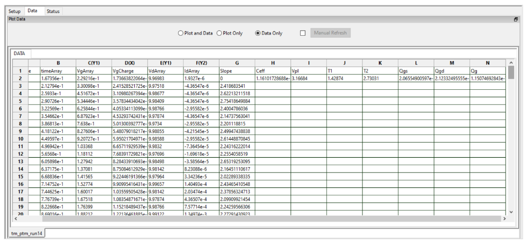
| Output Parameter | Description |
| gate_charge | Test status values - see Table 3 for descriptions |
| timeArray | Measured time (seconds) |
| VgArray | Measured gate-source voltage (volts) |
| VgCharge | Measured gate charge (coulombs) |
| VdArray | Measured drain voltage (volts) |
| IdArray | Measured drain current (amps) |
| Slope | Dynamic slope (dVg/dt) of gate voltage |
| Ceff | Ratio of gate charge to maximum gate voltage |
| Vpl | Plateau or Miller voltage (volts) |
| T1 | Timestamp where the plateau area begins (seconds |
| T2 | Timestamp where the plateau area ends (seconds) |
| Qgs | Gate charge from the origin to the first inflection point, or the voltage plateau (coulombs) |
| Qgd | Gate charge between the two inflection points in the gate charge curve (coulombs) |
| Qg | Gate charge from the origin to VgsMax (coulombs) |
Table 2: Output Parameters for gateCharge.py PTM
Checking the Test Status
Each time the test is run, a Test Status Value is returned to the first column in the Data Tab, titled: "gate_ charge". Table 3 lists the Test Status Values that may appear in the "gate_charge" column and their corresponding descriptions.
| Test Status | Description |
| 1 | No Errors |
| -1 | Gate SMU is not present |
| -2 | Drain SMU is not present |
| -3 | VgsMax > 200V |
| -4 | drainI exceeds 1A (HP SMU) or 100mA (MP SMU) |
| -5 | Power limit exceeded. Decrease drainI or drainV. |
| -6 | timeOut is out of range; set timeOut <300s |
| -7 | Test time exceeds specified time out. |
| -8 | Number of iterations >10000. Increase gate current. |
| -9 | Number of iterations <5. Decrease gate current. |
| -10 | Number of points from origin to first plateau point is <10. Decrease gate current. |
| -11 | Error calculating slope, S1. Curve not linear. Check test set-up and device. |
| -12 | Error calculating slope, S2. Curve not linear. Check test set-up. Reduce gate current. |
| -13 | Vds > 200V. Decrease drain voltage |
| -14 | gateCurrent > 1e-5 A. Decrease gate current. |
Table 3: Test Status Values
Integrated Solution with the 4200A-SCS Parameter Analyzer
For a comprehensive walkthrough using the all-in-one 4200A-SCS Parameter Analyzer with its integrated Clarius+ Software, see our dedicated application note: Measuring MOSFET Gate Charge with the 4200A-SCS Parameter Analyzer.
Conclusion
The inclusion of gate charge measurements in ACS software allows for the quality of devices such as power MOSFETs and IGBTs to be verified and validated with the ease and convenience of software. This no code solution to gate charge measurements also allows for easy viewing of data and the graph. With ACS Standard 6.2 or the Wafer Level Reliability edition, gate charge measurement tests can be used to verify the switching speed of devices at the wafer level.
Find more valuable resources at TEK.COM
Copyright © Tektronix. All rights reserved. Tektronix products are covered by U.S. and foreign patents, issued and pending. Information in this publication supersedes that in all previously published material. Specification and price change privileges reserved. TEKTRONIX and TEK are registered trademarks of Tektronix, Inc. All other trade names referenced are the service marks, trademarks or registered trademarks of their respective companies.
020823 11KW-73985-0