
Introduction
Semiconductor devices have not only advanced in capability but continue to dimensionally shrink. New devices are developed everyday that are used in applications we take for granted in tablets, phones, entertainment systems, avionics, space and defense systems, and autonomous vehicle systems. Many devices are used in mission critical applications where “failure is not an option”, once said by Gene Kranz during the Apollo 13 mission in his role as lead flight director. But device failures do occur.
Semiconductor companies and semiconductor researchers are constantly looking for ways to make devices fail to prevent them in the field. Semiconductor failure analysis (FA) engineers spend countless hours trying to understand why a device failed and how it can be prevented in the future.Failure analysis involves many different techniques.
Microelectronics failure analysis is one of the main analytical methods applied to the diagnosis of problems occurring with devices, either in the fabrication phase or in the use of the package in the application. The need of performing failure analysis spans across several applications within different markets. Microelectronics devices are integrated architectures made of several different layers. The location of fault in some cases is not simply two-dimensional but threedimensional.
A semiconductor device electrical failure can be either functional or parametric. When a device is unable to perform its intended function, this failure is considered a functional failure. A parametric failure is when the device is unable to meet electrical specifications for a measurable characteristic. A typical parametric failure can be leakage current, which may not pertain to the device's functionality. Thus, it is possible that a parametric failure may be present even if the device is still functional or able to perform its intended function.
How is Failure Analysis Performed?
The process of failure analysis starts with verifying the failure. Verification can also be performed to characterize the failure mode that describes how a device is failing. This most often provides a value that quantitatively says how far a specification is from its intended value. Simple verification tests typically would involve using a source measure unit (SMU) where you can ramp up to an I-V curve anomaly and then use the SMU to seamlessly creep into the behavior, minimizing the risk of further damaging a (potentially) already damaged device.
Keithley's I-V Tracer Software leverages the unique touchscreen interface of the 2400 Series SourceMeter® SMU instruments to recreate the familiar user experience of a curve tracer for two-terminal devices. Adding the I-V Tracer to your SourceMeter instrument gives you a dedicated user interface for tracing the characteristics of your devices through both current and voltage. With a range of compatible instruments, I-V Tracer can utilize the full capabilities of each source measure unit, including the dual high-speed digitizers of the Keithley 2461 SourceMeter instrument to perform tracing with AC polarity and pulsed DC, in addition to standard DC polarity. Using the right tools and good characterization of the failure mode is necessary to make the FA efficient and accurate.
After the failure has been verified, the FA engineer will proceed to subject the device to various FA techniques.This is a step-by-step process for collecting attributes of the failure and other observations along the way.
These techniques are categorized into two types, destructive and non-destructive. The objective is to determine the failure mechanism that led to the failure mode of the device. These failure mechanisms can come from potential fault lines in ICs from local heat dissipation, shorts between power or signal lines, oxide or junction breakdowns, latch-ups and much more. Unfortunately, destructive testing usually is necessary in a large portion of the analytical effort. Tasks such as decapsulation, scribing metal lines, and cross sectioning are some of the techniques used. Performed prematurely, however, these procedures can result in irreversible damage and a ruined analysis, ignoring the cost of the resources. But it may be the only way to understand what the real failure mechanism is.
Because of the risks of destructive testing, non-destructive testing is desired and done before considering destructive techniques. The good news is that new non-destructive techniques are being developed that help the failure analysist get to root cause faster.
Nondestructive evaluation of failures has historically been a visual process, using tools like transmission electron microscopy and other x-ray inspections systems. These tools come at a very large price tag. Another technique that is cost effective is Lock-in Thermography (LiT). LiT addresses a number of pain points that customers have:
- Don't want to destroy valuable devices under test (DUT).
- Need an easy way to periodically modulate the amplitude of the power dissipated in the DUT.
- Isolate problem sites or hot spots in packaged devices faster, reducing costs and getting to answers faster.
The process and physical principles behind thermography are indeed simple: the device under test has to be stimulated by an electrical source, while a thermographic sensor collects visual data to be furtherly processed.
Why Lock-in Thermography?
Lock-in thermography is an active thermography technique used to analyze microelectronic devices or more general samples of materials in order to detect defects, damages, or characterize potential fabrication issues. LiT allows the contactless measurement of surface temperatures using an infrared thermal imaging camera. The “lock-in” part of the name comes from the requirement to sync the camera's acquisition rate with the excitation of the circuit.
Lock-in thermography is a step up of standard thermal imaging fault location. It applies a technique to go beyond the detection limits increasing the resolution and sensitivity of the methodology in a massive way.
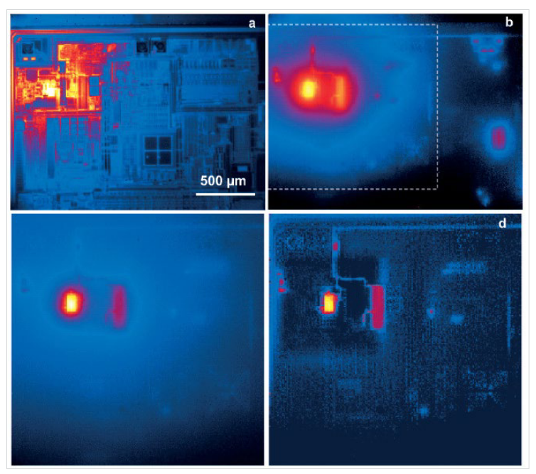
In short, this technique consists of applying a periodic thermal excitation to a device under test in the form of a pulsed electrical signal, then monitoring the temperature variation with a thermal camera which captures multiple fast acquisitions and computes these with a post processing algorithm. For semiconductor package devices, this enables the failure analysis engineer to map the surface of the package and identify localized hotspots with increased resolution and temperature distribution on the surface of the package. This speeds up the ability to locate faults for deeper analysis, saving time and money
The camera acquisitions are digitally processed in a specific way. This application is a perfect example of conjunction between electrical metrology and thermal imaging.
How Tektronix/Keithley can help to build an effective solution for Lock-in Thermography
One of the basic components of a lock-in thermography system is the “pulsing section”, i.e., the modulated bias source that induces the thermal emissions to the device under test which needs to be precisely controlled by a lock in frequency generator.
A typical lock-in thermography system diagram would look like what is shown inFigure 3.
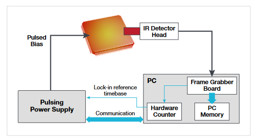
The above application could be addressed using a programmable arbitrary function generator, voltage pulse source, or a current source generator where appropriate, instead of the hardware counter and the pulsing power supply. When using any of the different sources, it's important that you understand possible pulse width limitations or excessive sourcing scenarios that could result in additional damage to the device. Current pulsers, for example can output current pulses as high as 10 amps at 10 volts with very small pulse widths. On the optical side, state-of-the art IR thermal cameras can be used in place of the IR detector and even the frame grabber. Specialized software is available for Lock-in Thermography, eliminating the need for the frame grabber to quickly display and analyze the data from the IR camera. As some thermal power heats up the internal structure of the device or is originated by the operating conditions of the device, thermal power is also dissipated, containing information over potential electrical defects. This is where the measurements of a thermal camera come into play
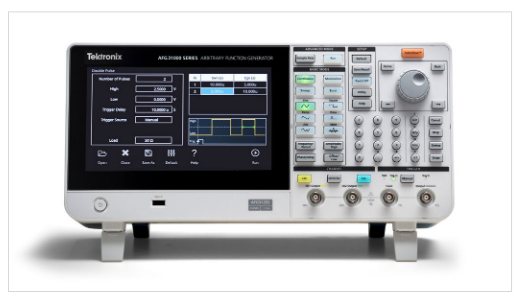
As for the arbitrary function generator, which could be used as a very precise clock or for outputting voltage pulses to an amplifier, the Tektronix/Keithley AFG31000 Series offers the combination of ease of use and programmability at a wide frequency range.
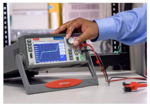
For a voltage source, Keithley source measure units, like the SMU shown in Figure 1, make ideal instruments.SMUs can act as precise voltage sources, can quickly change their output between different levels, and can limit delivered power in the event of a breakdown faster than power supplies. Because SMUs can measure both current and voltage simultaneously, they can trivially measure total power delivered.
For the current source models, there are a number of models available depending on the voltage and current ranges required to directly drive a component or even a laser source.
Failure analysis engineers continue to look to streamline the test system to minimize difficult integration challenges.One of the key requests however was to have an all-inone instrument including a built-in programming function to coordinate the process and lock-in function with the thermal camera.
Reacting to the challenges we heard from FA engineers,Keithley – a Tektronix Company – developed the new 2601B-PULSE System SourceMeter® 10 μs Pulser/SMU Instrument.
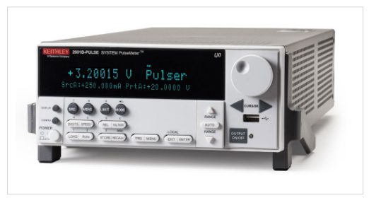
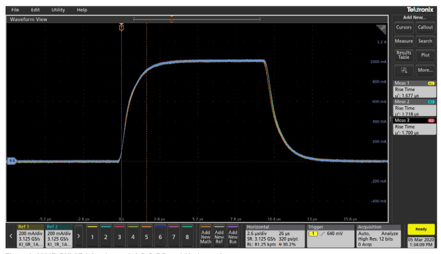
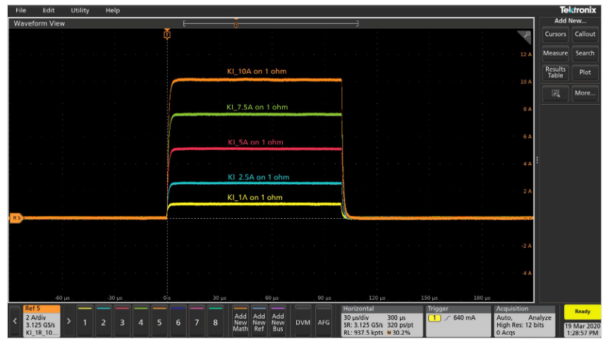
The new 2601B-PULSE with PulseMeter™ technology is a high current/high speed pulser with measurement capability plus the full functionality of a traditional source measure unit. This new pulser offers leading 10 A current pulse output at 10 V with a pulse width minimum of 10 μs, perfect for applying pulse stimulus at varying current levels to packaged parts for Lock-in Thermography. The 2601B-PULSE's control loop system ensures stable current pulses from 10 μs up to 500 μs with fast rise times (typically <1.7 µs), so your devices are sourced and/or stimulated with a high fidelity current pulse as shown inFigures 6 and 7.If the application requires pulse widths from 500 μs to DC, you can use the SMU function to generate longer pulses. This makes the instrument a great resource for many phases of failure analysis, including the failure verification process by running I-V sweeps on the questioned device.
The instrument also has a built-in timer function that eliminates the need for an external time reference. The internal timer has a free running 47-bit counter with 1 MHz clock input. The timer resolution is 1 µs and accuracy of ±100 ppm. Based upon the diagram inFigure 3, the 2601B-PULSE replaces the pulsing power supply and the hardware counter.
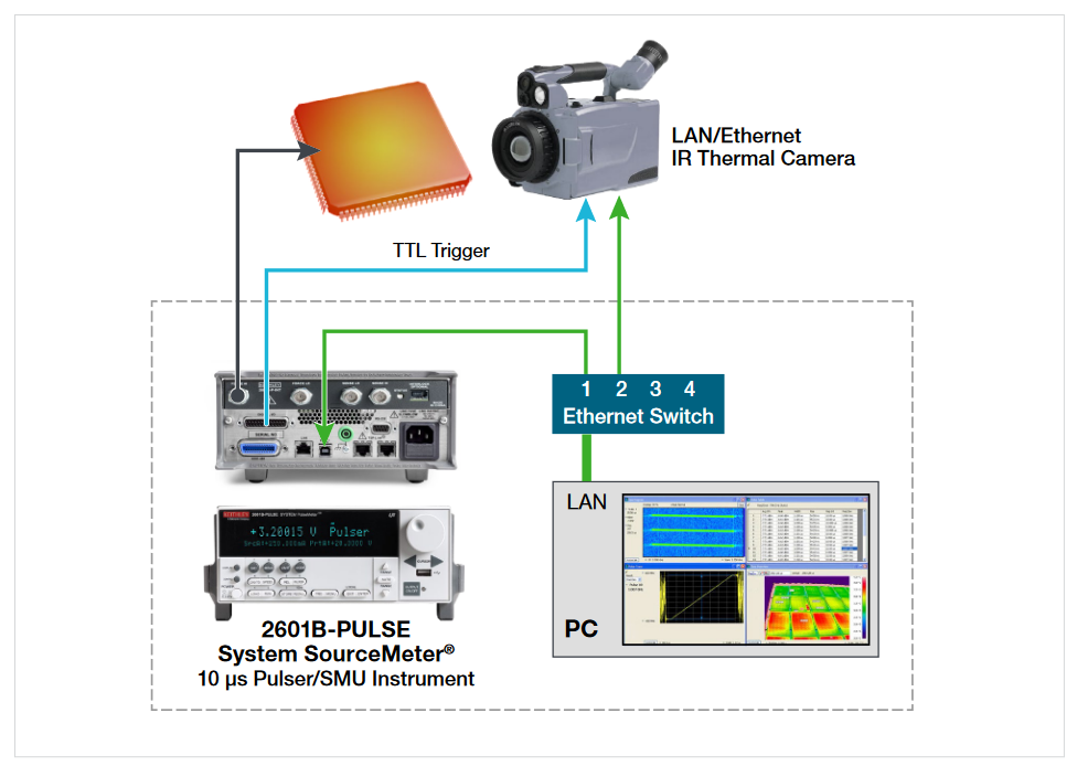
The 2601B-PULSE offers several I/O interface such as USB 2.0, LAN, GPIB, RS-232, and digital I/O. If the FA engineer chooses to use an advanced IR camera instead of a frame grabber and a hardware IR detector sensor, and the IR camera has a built-in LAN port to communicate to the PC, the 2601B-PULSE can provide the trigger pulses to the camera for the synchronization. This can speed up test execution leaving the external computer dedicated for image processing.
The Pulser/SMU incorporates Keithley's Test Script Processor (TSP™) technology, a flexible hardware/ software architecture that allows message-based programming with enhanced capabilities for controlling test sequencing/flow, decision-making, and instrument autonomy. The use of the on-board Test Script Processor has made it possible to create “smart” instruments, with built-in decision making capabilities, which reduces the need to communicate so frequently with an external controller over the bus. This approach to test system design allows smart instrument systems to be much more efficient than those that rely on standard SCPI based programming. But how do you control a LAN available IR Camera?
TSP-Net
With Keithley TSP-Net, an included library of TSP, you can use TSP-enabled instruments to control any ethernet controllable instrument. Using this feature, measurement instruments can be controlled remotely by other instruments without a PC. This type of setup is especially convenient when instrument lacks a front panel or requires navigating through settings with numerous buttons or knobs. To set up a TSP-Net connection, connect the desired instruments to the same network or to one another via ethernet cable and upload a TSP-Net script onto the controlling instrument.
TSP-Net works similarly to sockets-based programming between a computer and an instrument. Instead of using a PC, one of the instruments connected to the network acts as the controller, driving the target instruments through a TSP script via an ethernet network connection. This allows one or more instruments that are not necessarily located in the same immediate area to control the others remotely and communicate with each other. The controlling instrument uses commands from the TSP-Net library to transfer string data, including commands, to a remote instrument. In the same way, the controlling instrument can retrieve and manipulate data from the target instruments. Because strings are sent over the bus, a TSP instrument can send SCPI commands, which are strings of ascii characters, to an instrument that is not TSP compatible with a script using TSP-Net.
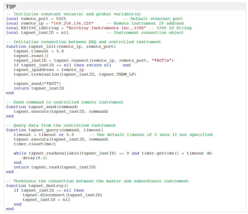
This following example demonstrates the main coding structures and commands associated with the use of TSPNet. Note the similarities between these commands from the TSP-Net library and typical sockets based programming:
By using the 2601B-PULSE Pulser/SMU with a LAN/Ethernet enabled IR thermal camera, you can simplify the Lock-in Thermography configuration and allow the 2601B-PULSE to control the testing process while the PC runs the thermal analysis software as shown in Figure 9.
Conclusion
At the end of the day, the job of the FA engineer is to determine the failure mechanism that led to the failure mode of the semiconductor device package. As soon as the failure mechanism has been determined, the FA engineers can work with the semiconductor process engineer to determine the root cause and the countermeasures that will be executed to prevent the failure from re-occurring.
Lock-in Thermography is just one technique for quickly identifying hotspots on the device to narrow down the location of a failure and continue the investigation to determine root cause. Instruments like the Keithley 2601B-PULSE and an LAN/Ethernet enabled IR thermal camera minimize the challenges of integrating advanced instrumentations to conduct the measurements. Lock-in Thermography reduces the need for destructive testing and helps to overcome the challenges that failure analysis presents at the package level, resulting in faster time to answer, more efficient use of the FA engineer's time, and cost savings to the organization.
To learn more about the instruments highlighted in this White Paper, please click on the following links: