Abstract
This paper compares two-port S-parameter responses extracted from vector network analyzer (VNA) measurements and time domain reflection and transmission (TDR/TDT) measurements up to 20 GHz, and demonstrates excellent correlation between the two methods. The measured devices consisted of various via structures and a microstrip trace on a printed circuit board. To de-embed the launch effects, the VNA measurements used on-board Thru-Reflect-Line (TRL) calibration while the TDR/TDT measurements used Thru and Open references. The Sparameters from TDT/TDR measurements were extracted using TDA Systems IConnect. Parameters for VNA and TDR measurement such as IF bandwidth, number of points, sampling interval, acquisition time window, and number of averages were optimized.
This paper is a presentation of empirical data,demonstrating TDR/TDT as an alternative network analysis and more accessible methodology for obtaining Sparameters, compared to VNA, which will be helpful to engineers who work in high-speed digital technology.
Keywords
VNA, TRL, TDT, TDR, S parameters.
INTRODUCTION
We perform measurements to understand the behavior of a device or a system, to debug, to verify our model, etc. Although measurements give the most accurate behavior of a device, it is not always straightforward to achieve accurate measurements, especially at high frequencies. To make measurements, the “Device Under Test” (DUT) is generally inserted into a fixture or between probe launches. It is necessary to de-embed the effects of any instrumentation or fixtures such as cables, probes, PCB traces, etc., separate from the device. Calibration standards are usually required to de-embed the effect of these fixtures properly from VNA measurements. The accuracy of the measurements depends on the quality of calibration standards and the accurate characterization of these standards.
Vector Network Analyzers have historically been used for network characterization. They measure reflection and transmission characteristics of a system as functions of frequency. However, de-embedding non-DUT (instrumentation, fixturing) effects from VNA measurements is complex and prone to error. Furthermore,network analyzers are very expensive, not intuitive for a digital designer or an engineer who is inexperienced in measurements, and require demanding calibration structures and procedures. They are therefore considered ill suited for many designers’ needs.
TDR measurements are commonly used for board characterization to determine characteristic impedances of board traces. TDR measurements provide spatial resolution for the device-under-test, and therefore the interconnect discontinuities can be observed and windowed effectively. TDR measurements, however, require good time resolution to observe electrically small devices. Digital designers are accustomed to TDT/TDR measurements. But, their dynamic range limitation and lack of frequency-domain information (which is required to study conductor and dielectric loss effects, for instance) have precluded their use for state-of-the-art measurement of PCB interconnects.
There are now methods available to easily extract frequency data from TDR/TDT measurements. Measurement instrumentation must still meet the dynamic range and bandwidth requirements for testing purposes, but for most practical digital interconnect structures, TDR equipment has adequate dynamic range. The data in this paper indicates that TDR/TDT measurements are a viable and attractive alternative to directly measuring S-parameters with VNA, for many common digital interconnect structures.
VNA & TDR BASICS
There are many good references available regarding theories on VNA and TDR basics. [1-6]
VNA On-board TRL Calibration
The TRL method is generally used in high frequency measurement because the characteristics of test standards do not have to be completely known. TRL calibration relies on transmission lines rather than a set of discrete impedance standards. The reference plane can be set at desired position using “Thru” or “Reflect” standards. A “Line” standard provides reference impedance. Multiple lines are needed for broadband coverage in the VNA measurements. The frequency of interest for this experiment is from 200 MHz to 20 GHz. For this frequency range, three line standards are needed. [2] However, the conventional TRL method has limitations.
The calibration is not valid at all frequencies: the calibration can fail at frequency break points of each line.Also, impedance variation of traces induces error,especially in return loss. [9]
TDR and IConnect™
The IConnect® software operates on time domain measurements, using Time Domain Network Analysis (TDNA) and a duration-limited FFT algorithm to compute S-parameters from the TDR/TDT measurements with appropriate step references. The insertion and return losses of the DUT are easily calculated from TDR/TDT measurements of “reflect” and “thru” reference structures, and the DUT. It theoretically de-embeds fixturing contributions with selection of proper reference measurements. [7]
TEST BOARD & TEST STRUCTURES
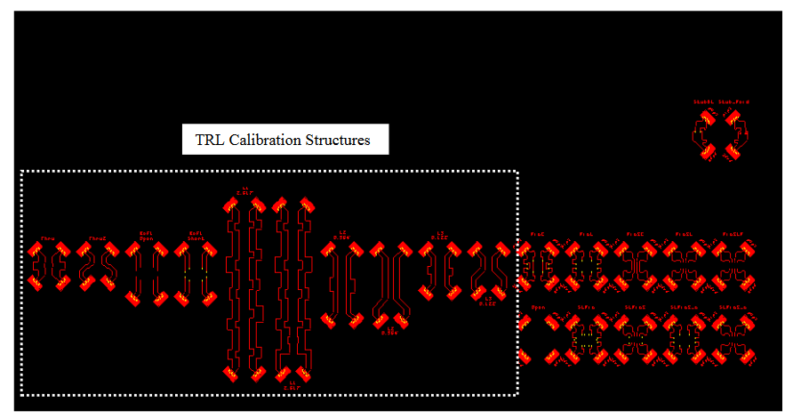
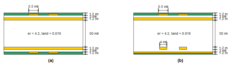
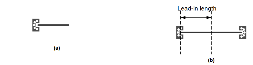
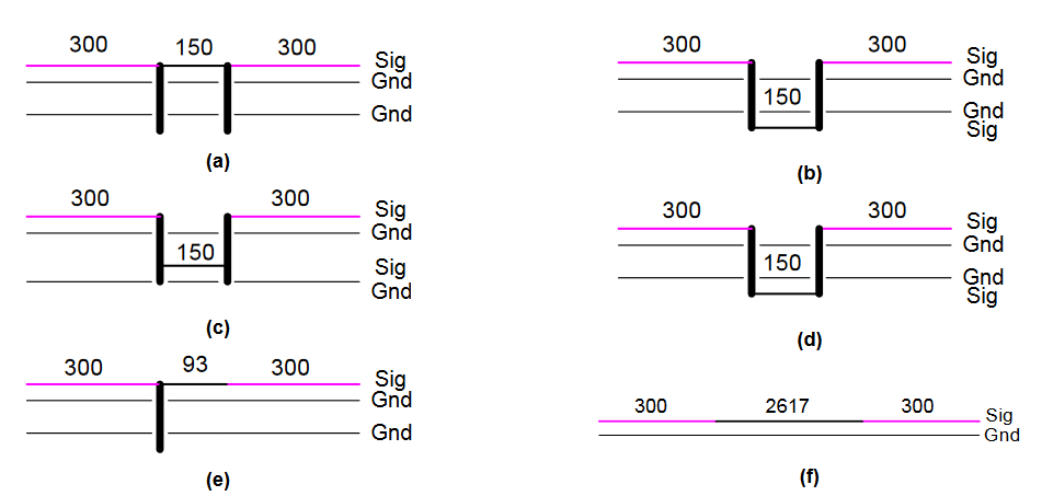
The original purpose of this experiment was to characterize various via structures using VNA. The test board is a fourlayer board with various via structures and microstrip traces, and includes two different cross-sections for microstrip and stripline structures. The board layout and its cross-sections are shown in Figure 1 and Figures 2(a) & (b). Figure 4 illustrates the features of the various test structures. With their various geometries and topologies, they give complex responses (many resonances, etc. at various frequencies) over a bandwidth of 20 GHz. The board is built using FR4 and designed to have an effective dielectric constant of approximately 4.2 and a loss tangent of 0.018. The test structures are accessed using PicoProbes [11] and microstrip lead-in traces before and after the “reference planes” (points at which the DUT begins and ends). The picoprobe launches and the reference plane diagrams are shown in Figure 3(a) & (b).
MEASUREMENT PARAMETERS
For the measurement procedures in this experiment, the critical parameters are the IF bandwidth and number of data points for the VNA setup, and sampling interval and acquisition window length for the TDR setup. The number of data points, window length, and number of averages are related to the dynamic range of the measurement data.
VNA
IF Bandwidth
The network analyzer converts the received signal from its source to a lower intermediate frequency (IF). The bandwidth of the IF bandpass filter is adjustable from 40 kHz to minimum of 1 Hz. Reducing IF bandwidth reduces the effect of random noise on a measurement resulting in higher dynamic range with the trade-off in sweep time.
Number of Points
The higher number of points corresponds to the smaller frequency step. The number of data points used should be large enough to achieve a good resolution. Sweep time changes proportionally with the number of points. There is significant decrease in computer processing speed with increased number of points. To ensure an accurate measurement calibration, the calibration should be performed with the same number of points that will be used for the DUT measurement.
TDR
Sampling Interval
The sampling interval should be small enough to capture the rise time of the source properly. If there are not enough data points to track the rise time, the relevant frequency information on the source and the device cannot be extracted. In general, the number of points is set to maximum allowable number, which will achieve the best possible time resolution of the measurement.
Acquisition Window Length
It is important to window the DUT waveform properly. The incident edge of reference waveform and DUT waveform should always occur at the same time relative to the trigger. The window should not capture the incident edge but only the reflected edge. The DUT waveform should settle to steady DC level in the window. [8]
Increasing the length of time in the window achieves better resolution in frequency response. (frequency step = 1/window length).
Averaging
Averaging reduces the effect of random noise. Increasing digital averaging in the scope has the same effect as narrow band (IF) filtering in a VNA. Increasing averaging two times increases the dynamic range by 3 dB.
Increasing the number of points and decreasing acquisition window also have the same effect. The relation between dynamic range (DR) and number of points, number of averages and window length can be described by the following equation. [8]
EQUIPMENT SETTINGS
VNA Setting
Agilent Technologies E8362A PNA Series VNA (45 MHz – 20 GHz) was used to perform 2-port measurements. The VNA was set up as follows: fstart = 50 MHz, fstop = 20 GHz, Number of Points = 401, IF Bandwidth = 500 Hz. A full 2-port on-board TRL calibration was performed. The measurements of test structures were taken.
TDR Setting
The transient responses were captured using Tektronix TDS 8000 Digital Sampling Oscilloscope and Tektronix 80E04 Sampling Module with 17 ps rise time. The effective rise time of the input step at the end of the cable was measured to be 29 ps.
The TDT of the “thru” calibration structure was measured and stored as a thru reference. The TDR of a reflect “open” calibration structure was measured and stored as an open reference. Reflection and transmission measurements of test structures were taken.
TDA Systems’ IConnect™ was used to extract S-parameters from time domain measurements. S21 was calculated using the thru reference measurement as the step and TDT measurement as the DUT. S11 was calculated using the open reference measurement as the step and TDR measurement as the DUT.
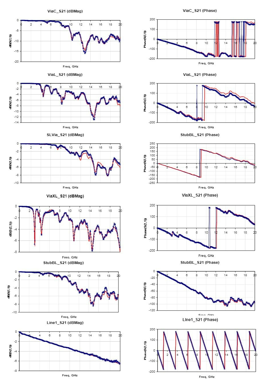
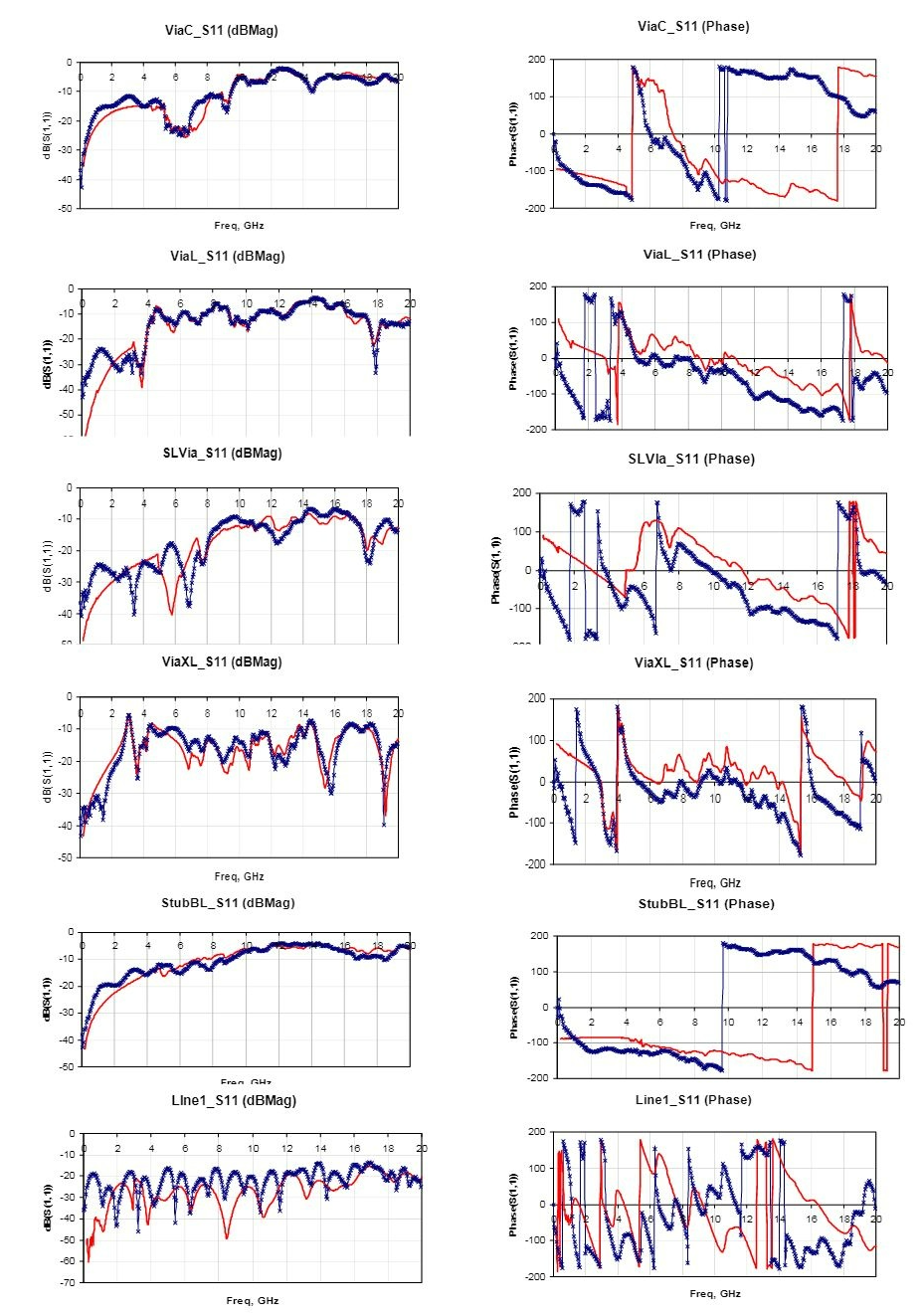
MEASUREMENT DATA & COMPARISON
We performed the on-board 2-port TRL calibration and took the measurements of different structures. We then used TDR as an alternative and extracted S-parameters using IConnect™. The measurement data and comparison of two methods are shown in Figure 5 and 6. The plots show that the two results are highly comparable – remarkable in some cases. The S21 magnitude and phase match very well up to 20 GHz, and the S11 data matched respectfully in most cases. The S11 results for TDR might be more accurate than these VNA results due to the induced error because of the impedance variations and band limited line calibration procedure.
CONCLUSION AND FUTURE WORK
In this paper, we described the transient methodology for obtaining S-parameters and compared results with those of vector network analyzer measurements up to 20 GHz. The insertion loss extracted from both methods matched closely, and the return loss matched reasonably well in most cases. With proper reference measurements (thru or open), fixture or launch contributions can be de-embedded using commercial software such as IConnect™. There are several benefits to using TDR vs. VNA:
- TDR/TDT measurements are much more straightforward to acquire
- TDR gives immediate feedback if a good contact is established between the probe and the trace during reference and DUT measurements, while with VNA it is not transparent to the user during calibration.
- Time Domain waveforms are much more intuitive to understand, to determine the effects of different aspects of a particular DUT
The 29 ps risetime provided adequate resolution up to 20 GHz. The ease of the calibration structures and measurement procedure, together with related expenses of VNA, have led us to consider time domain measurement as an alternative for obtaining frequency domain data in this range.
The next step will be to validate the accuracy and dynamic range of the TDR/TDT measurements for different launch structures, different electrical lengths, and higher frequencies. This would serve to better characterize the device or system at higher frequencies.
We target this paper towards the audience of digital engineers and hope that this paper will help the board manufactures and designers to better characterize the printed circuit board at higher frequencies.