This tutorial explains the importance of electrical measurements to the science of nanotechnology, and presents practical considerations in making these measurements. Topics include material and structural characteristics that can be explored with electrical measurements, and why these measurements are important for even non-electronic nanoscale materials, such as those used in structural and biological applications. The tutorial then explains how to of source-measure instruments with nanomanipulators.
Testing for Unique Properties
Like the testing of other engineered materials, measurements made on substances created with nanotechnology are aimed at discovering useful properties. Generally, the relevant properties relate to specific applications or products. For bulk materials, the bulk properties of interest may include tensile strength, phase transition temperature weight, hardness, electrical and thermal conductivity, etc. Nanotechnology offers ways to create new materials that have improved properties for applications such as structural members, electronic circuit elements, optical devices, and a host of other uses [1]
In some respects, the testing of bulk materials and those created with nanotechnology are similar. However, the nature of nanotech materials requires some novel testing techniques. Since these materials are built at the atomic or molecular level, quantum mechanics come into play. As a result of small particle sizes, the atoms and molecules of these new materials may bond differently than they might otherwise in bulk substances. There may be new electronic structures, crystalline shapes, and material behavior. Nanoparticles with these new properties can be used individually, or as building blocks for bulk material. While the discovery of bulk properties remains important, measurements also need to uncover the characteristics unique to na-noscale structures
An excellent example is the carbon nanotube (CNT). CNTs can be manufactured to consist of a single sheet of carbon atoms oriented in a graphite-like structure, rolled up into the shape of a tube only a few nanometers in diameter [2]. The smallest diameter tubes are insulators (i.e., large bandgap materials). As the diameter of the CNT increases, its bandgap decreases. With a large enough diameter, a CNT can become a semiconductor. At even larger diameters, CNTs exhibit metallic properties, acting like conductors.
Structure and Behavior of the very small
Particle size and structure have a major influence on the type of measurement technique used to investigate a material. Macroscopic materials can be viewed with optical microscopes. For nanoscopic materials with particles smaller than 200 nanometers, a scanning tunneling microscope (STM) or an Atomic Force Microscope (AFM) can be used. Table 1 outlines the relative sizes of particles considered as nanoscopic, mesoscopic, and macroscopic.
| Classification | Particle Size |
| Macroscopic | >300nm |
| Mesoscopic | Varies with phase coherence length |
| Nanoscopic | 0.5 - 200nm |
| Atomic | <0.5nm |
Table 1. Relative sizes of various particle classifications
SEM, STM and AFM techniques are particularly useful for crystalline nanoparticle structures. Figure 1 illustrates the atomic structures for some typical crystals with well-known forms, such as simple cubic (SC), body-centered cubic (BCC), or face-centered cubic (FCC). Knowing the arrangement of atoms in those structures helps predict a particle's properties. However, on
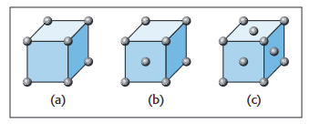
a nanoscopic scale, it is the particle's size that fundamentally alters the physics of its behavior and dictates the use of other measurement methodologies.
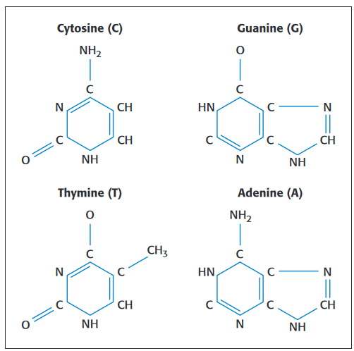
Two important sets of properties change as particle sizes are reduced to nanometer dimensions, i.e., the material's chemical and electrical characteristics. This even applies to biological materials. (See examples in Figure 2.) Therefore, most of these materials require chemical and electrical testing to characterize them for practical product applications. For many of them, the actual quantity being measured is a low level current or voltage that was translated from another physical quantity [3]. Direct electrical measurements are possible on many nanoscopic substances with probing instruments and nano-manipulators now available.
Electronic properties
As a substance is reduced to nanoscopic dimensions both the band gap and the distance between adjacent energy levels within the material's electron energy bands are altered. These changes, along with a particle's nanoscopic size with respect to the material's mean free path (average distance an electron travels between scattering events), directly affect the electrical resistance of a nanoparticle. More generally, a material's bandgap directly influences whether a particle is a conductor, an insulator, or a semiconductor.
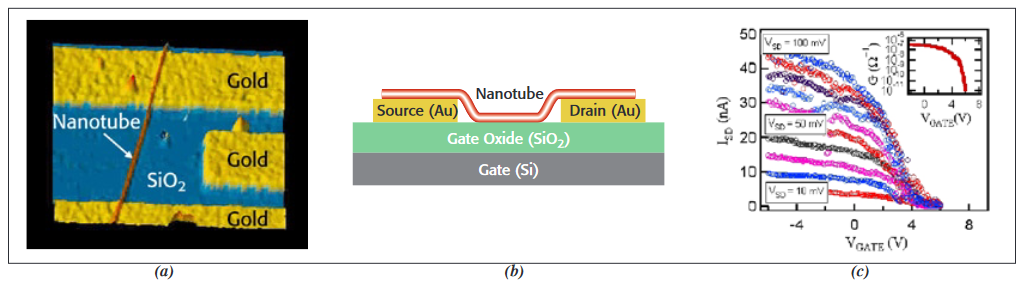
These influential electronic properties allow, for example, a CNT to be used to create a transistor switch [4]. One way to do this is by connecting a semi-conducting CNT between two electrodes that function as a drain and source. A third electrode (the gate) is placed directly under the entire length of the carbon nanotube channel (Figure 3). For a semi-conducting CNT, the introduction of an electric field through the channel (via the insulated gate placed in proximity to the CNT channel) can be used to change the CNT from its semi-conducting state to its insulating state by increasing the gate voltage. Decreasing the gate voltage will transition the device into a conducting state. (See Figure 3b and earlier text on CNT bandgap and conducting states.) This conduction mechanism is analogous to the operation of a silicon MOSFET transistor switch, which is created by doping silicon with either an electron acceptor or donor to alter the material's electronic conductivity in specific localities. (Additional information on CNTs is available from IBM Research Division, Nanoscience Department [5].)
Properties Associated with Electrical Measurements
For macroscopic sized particles, electrons take on discrete quantums of energy that lie within energy bands, each band consisting of many energy levels that electrons can share through their thermal energies. For a conducting material, electrons can be thermally excited into the conduction band, i.e., electrons are present in the valence as well as in the conduction band. For an insulator (bandgap > thermal energy of the electron), an enormous energy is required for an electron to transition from the valence to the conduction band separated by the material bandgap If a suitable amount of energy is absorbed (> bandgap), then electrons can jump bands.
As a particle's size is reduced to nanoscopic dimensions, the allowable energies within the continuous bands separate into discrete levels (since there are far fewer atoms in the mix). This occurs when the separation between energy levels approaches the thermal energy of the electrons. See Figure 4. With fewer energy levels within the specific energy band, the density of states of the material changes.
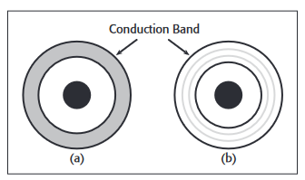
The density of states is a measure of the number of energy options available to an electron as it falls into a lower energy level by giving up energy, or as it ascends to a higher energy level after absorbing energy. A corollary is that if the density of states is known, the size of the particle can be deduced.
The density of states can be used to engineer characteristics of a nanoscopic particle, particularly a metallic or semiconducting particle. For example, these materials take on color by selectively absorbing and reflecting light wavelengths. If the material cannot absorb photons with certain wavelengths because its density of states has changed (removing critical energy levels associated with absorption), then the color of the material will change
If a particle becomes small enough, its physical size may approach the wavelengthof the material's electrons. Quantum size effects must be considered whenever a particle approaches this critical dimension. Because of quantum mechanics, the energy of its electrons cannot be predicted by the bonding normally associated with the bulk material.
Nevertheless, electron energy effects can be deduced from electrical measurements when nanoparticles take part in a chemical reaction of the oxidation-reduction (REDOX) type, such as the chemical-electrical conversion that takes place in fuel cells or batteries. Briefly stated, every reaction of this type is associated with the transfer of a specific number of electrons from one species to another. The number of electrons transferred depends on the specific reaction(s) taking place, and on the frequency of the reactions (reaction rates). Electrical measurements of the transferred electrons can be used to determine reaction rates by tracking the current and potential of the cell, with time. Reaction and conduction measurements are then used to track particle size, density of states, reaction rates, and other nanoscopic properties.
Determining the Density of States
Characterizing the density of states is a fundamental activity in nanoscopic material research. Density of states (3D dimensionality) as a function of energy can be expressed as
This represents the number of electron states per unit volume per unit energy at energy E, where m represents the effective mass of the particle, h is Plank's constant, and E is the energy (electron orbital location) in electron volts. While the result is independent of volume (can be applied to any size particle), this equation is of limited value if the particle size/structure is unknown. However, there are other ways to determine the density of states experimentally from which the particle size can be found. The 0D and 1D density of states as applied to nanoparticles are discussed below.
X-ray spectroscopy
The density of states can be measured by bombarding a material with electrons. The energy of the bombarding electrons excites the material's electrons into higher energy
levels. X-ray emission takes place as these electrons return to lower energy levels. The x-ray emission energy indicates the difference between the energy level harboring the excited electron, and the level that recaptures the electron after the emission. Fewer energy levels mean fewer electrons are excited, yielding lower radiation intensities as they return to lower energy states. A spectrographic analysis of the resulting x-ray emission energies and intensities vs. the bombarding electron energies reveals the density of states for the material
Direct electrical measurements
Since the density of states can be used to predict the electrical behavior of materials, it is also possible to use electrical impedance measurements to derive density of states information. Prior art has used a scanning tunneling microscope (STM) to tunnel a current through a nanoscopic device. The density of states is found by plotting differential conductance vs. applied voltage. Differential conductance is simply (di/dv).
In this technique, the quiescent current vs. voltage characteristics are established through the STM's high resistance contact, with a low level AC modulation on top of the quiescent operating point to measure the differential conductance di/dv. When this conductance is plotted against voltage, the graph indicates the material's density of states.
Highly conductive materials possess an abundance of free energy levels in the conduction band, i.e., greater density of states (more individual allowed energy levels per unit energy). Insulating materials have an electronic structure with a dearth of occupied energy levels in the conduction band. Since density of states corresponds to the density of these energy levels, a plot of conduction vs. voltage provides a direct measure of the electronic density of states at each energy level (voltage across the device).
SMU/nano-manipulator methodology
An alternate approach to this technique is to replace the STM and its high resistance contact with a nano-manipulator that makes low resistance contacts to the nanoparticle. Such an arrangement allows charge transport and density of states measurements without an STM. This works well into the conduction region thanks to the low resistance direct connections of the nano-probes on the material (particle) being tested
The nano-manipulator and its probes, along with a source-measure unit (SMU), are used to apply a current or voltage stimulus directly to the nanoparticle and measure its corresponding voltage or current response. (See Figure 5.) The advantage of electrical source-measure testing is rooted in the fact that a specific SMU measurement mode (source current/measure voltage or vice versa) can be chosen based on the relative impedance of the material or device under test (DUT). Furthermore, the measurement mode can change dynamically as the impedance changes, such as occurs in CNTs acting as semiconductor switches. This allows a much wider dynamic range of voltage and current stimuli and measurements, thereby optimizing parametric test precision and accuracy. SMU voltage and current sensitivity can be as good as 1 microvolt and 100 attoamp
Probing and Connection Issues
Electrical measurements on nanoscopic materials place stringent requirements on the instrumentation. In order to measure conductivity, impedance, or other electrical properties, and relate those measurements to the density of states, a galvanic connection must be made to the nanoscopic DUT [6]. This represents one of the major hurdles to be overcome in the field of nanotechnology testing. There are only a few tools available and few device constructs that facilitate connections of this type.
Often, nanoscopic particles are classified dimensionally in terms of exactly what it is about them that is small. Quantum wells represent material with nanoscopic measurements in only a single dimension, such as a thin film. Quantum wires are small in two dimensions (or diameter), and quantum dots are nanoscopic in all Cartesian coordinates.
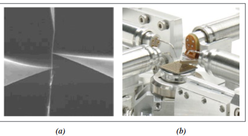
Particle self-assembly can be accomplished from silicon to silicon, where conventional photolithographic techniques are used to make electrical connection pads for probing. Particles that are long enough to straddle such pads (for example, carbon nanowires) can be connected to the pads through externally generated electrostatic fields. Figure 5 illustrates an example of this.
Although the properties of quantum wells, wires, and dots differ, it's possible that information about a particular material in the form of a quantum dot can be inferred by examining the same ma terial fashioned as a quantum wire or well (nano-film). Nano-films are particularly easy to measure since only one dimension is small. Such a film might be deposited on a conductive substrate, allowing measurements through the volume as well as over the surface, using appropriately placed macroscopic test pads formed on the material surface. For conductive materials, separate pads for source and measure can be deposited to create a Kelvin (4-wire) connection [7]. This type of circuit eliminates test lead resistance from the measurement and improves accuracy. In any case, a quantum well (nano-film) can be tested like any other bulk material.
A nano-manipulator and STM can also be used to make direct electrical connections to nanoparticles. STM do this by a tunneling current, established by closing the distance between the STM tip and the nanoparticle to within a single electron wavelength.
Electrical Measurement Considerations
Electrical measurements on passive devices (any device that is not a source of energy) are made by following a simple procedure: stimulate the sample in some way and measure its response to the stimulus. This method also works for devices that have both passive and active properties with linear or non-linear transfer functions. With appropriate techniques, a source-measure algorithm can be useful for characterizing sources of energy. Fuel cell and battery impedance spectroscopy are examples of such measurements.
For nanoscopic particles, this general method takes the form of source-measure testing to quantify impedance, conductance, and resistance, which reveal critical material properties. This test methodology is useful even if the end application is not an electronic circuit.
General Considerations
Important considerations in the characterization of nanoscopic particles include the following:
1. Nanoscopic particles will not support the magnitude of currents that macroscopic device can carry (unless they are super-conducting). This means that when a device is interrogated, the magnitude of a current stimulus must be carefully controlled.
2. Nanoscopic particles will not hold off as much voltage from adjacent devices as a conventional electronic component or material (such as a transistor). This is due to the fact that smaller devices can and are placed closer together, smaller devices have less mass, and they may be affected by the forces associated with large fields. In addition, internal electric fields associated with nanoscopic particles can be very high, requiring careful attention to applied voltages.
3. Since nanoscopic devices are small, they typically have lower parasitic (stray) inductance and capacitance. This is especially useful when they are used in an electronic circuit, enabling faster switching speeds and lower power consumption than comparable macroscopic devices. However, this also means that instrumentation for characterizing their I-V curves must measure low currents while tracking the short reaction time.
Speed, Sensitivity, and Accuracy
Since nanoscopic test applications often require low current sourcing and measurement, appropriate instrument selection and use is critical for accurate electrical characterization. Besides being highly sensitive, the instrumentation must have a short response time, (sometimes referred to as high bandwidth), which is related to a DUT's low capacitance and ability to change state rapidly at low currents. This was illustrated earlier in Figure 3c (I-V characteristics of a carbon nanotube used as a switch).
Measurement Topology
It's important to recognize that the switching speed of a source-measure test circuit may be limited by the instrumentation used to follow the state of the device. This is especially true if a non-optimal measurement topology is used to observe the device. The two possible topologies are source current/ measure voltage, or source voltage/measure current.
When considering the measurement of low impedance devices (less than 1000Ω), the source current/measure voltage technique will generally yield the best results. Current sources are stable when applied to lower impedances, and a good signal to noise ratio can be achieved without great difficulty. This allows accurate low voltage response measurements.
The alternative, source voltage/measure current, is not as well suited for low impedances. Exceptionally low values of applied voltage are required to keep device currents low and avoid destructive heating. At such low voltages, the source tends to contribute excessive noise to the measured current (response). In other words, the source's noise voltage is a significant percentage of the total applied voltage. Additionally, voltage sources are less stable with low impedance loads. There may also be current measurement problems related to an instrument's voltage burden (the voltage that develops across the input of an ammeter circuit), which introduces additional error.
When measuring high impedance devices (impedance greater than 10,000Ω), the source voltage/measure current technique is best. Stable voltage sources to drive high impedances are easily constructed. When a well-designed voltage source is placed across a high impedance, it will quickly charge the stray capacitance of the DUT and test cables and rapidly settle to its final output value. The small current response of the DUT can be accurately measured with an appropriate ammeter.
The alternative, source current/measure voltage, creates problems in high impedance measurements. To keep the voltage response low enough for practical measurements, this technique requires a low current value. This means that it will take a great deal of time to charge the device and cable capacitances. In addition, the high voltage measurement circuits will draw some of the source current from the DUT. Since the current is sourced,not measured, through the device, this current draw represents an error in the measurement
Electrical noise
Measurement topology also has an impact on electrical noise, which is the ultimate limitation on measurement sensitivity and accuracy. For low impedance voltage measurements with a current source, the measurement circuits will be sensitive to DUT voltage noise and impedance.
For macroscopic devices, such as a resistor, the Johnson noise voltage at room temperature (270ºK) is expressed as:

where
k = Boltzmann's constant,
T = Absolute temperature of the source in degrees Kelvin,
B = Noise bandwidth in Hertz,
R = Resistance of the source in ohms,which can be further simplified to:

This equation shows that as DUT resistance, R, decreases, the Johnson voltage noise generated by the DUT also goes down. Conversely, high impedance devices stimulated with a voltage source are limited by current measurement noise. The Johnson current noise of a resistor at 270ºK is:

indicating that the noise goes down as DUT resistance increases
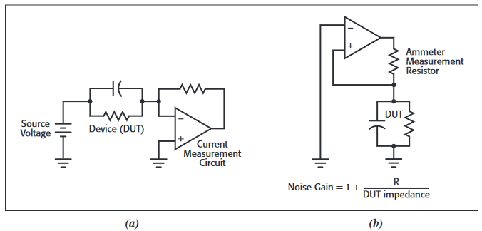
For all particle sizes, in addition to Johnson noise, there could be a noise gain associated with the measurement topology chosen.Noise gain is a parasitic amplification of the noise of the measurement system that is not present when the correct measurement topology is chosen. For example, consider a source voltage/measure current topology. An operational amplifier is used in many current measurement (ammeter) circuits, as shown in Figure 6. To minimize noise gain, the ammeter circuit must operate at a low gain with respect to its non-inverting input terminal.
Source-Measure Instruments
A commercial DC source-measure unit (SMU) is a convenient test tool for many nanoscopic material and device measurements. SMUs change measurement topology automatically, i.e., rapidly switch between source voltage/measure current and vice versa. This makes it easier to minimize measurement noise while maximizing measurement speed and accuracy.
As described earlier for a carbon nanotube, some nanoparticles can change state with the application of an external field.When investigating such materials, an SMU can be configured to source voltage and measure current for a nanoparticle in its high impedance state. When the material is in its low impedance state, more accurate results are achieved by sourcing current and measuring voltage. Furthermore, the SMU has a current compliance function that can automatically limit the DC current level to prevent damage to the material or device under test (DUT). Similarly, there is a voltage compliance function when current is being sourced
When using the compliance function, an SMU will satisfy the source value unless the user's compliance value is exceeded. For example, when an SMU is configured to source voltage with a preset current compliance, if that compliance value is exceeded, the SMU automatically starts acting as a constant current source. Its output level then will be the compliance current value. Alternately, if the SMU is set to source current with a compliance voltage, it will automatically switch to sourcing voltage (the compliance voltage) if the DUT impedance and the current it draws begin to drive the voltage higher than the compliance value.
While a nanoscopic device, such as a CNT switch, can change states rapidly, the change in instrument state is not instantaneous. Depending on the SMU model, the switching time can range from 100ns to 100μs. Although such switching speeds are not fast enough to track a nanoparticle as it changes state, the time is short enough to allow accurate measurements of both states while limiting DUT power dissipation to acceptable levels.
Pulsing techniques
Choosing the correct measurement topology to improve measurement speed and minimize noise may still fall short of the test needs for some nanoscopic materials. For example, it appears that some CNTs can switch 1000 times faster than conventional CMOS transistor switches. This is too fast for the nano-amp ranges of commercial picoammeters. Demanding devices such as these may require other techniques to improve the speed of impedance measurements.Low power pulsing techniques may offer a partial solution to this problem, and are available in some SMU designs. The idea is to use a much higher test current or test voltage and apply this large stimulus for a short sourcing cycle. The larger stimulus will lower the sourcing noise (by improving the signal-to-noise ratio) and improve the rise or settle time for a voltage pulse or current pulse respectively. Quieter sources require less filtering and permit a shorter sourcing cycle time (narrower pulse width). A larger source stimulus also increases the response current or voltage so that higher instrument ranges can be used, further minimizing the effects of noise. Since there is less noise, the measurement acquisition time (integration period) can be shortened, thereby speeding up measurements.
Avoiding self-heating problems
A possible source of error is self-heating due to excessive electrical current through the DUT. Such currents may even lead to catastrophic failure of the sample. Therefore, instrumentation must automatically limit source current during device testing.Programmable current and voltage compliance circuits are a standard feature of most SMU-based test systems with pulsed current capabilities, and may be required to avoid self-heating of some low resistance structures
When an elevated test current is required, it must be sufficiently brief so that it does not introduce enough energy to heat the DUT to destructive temperatures. (Nanoscopic devices tolerate very little heat, so the total energy dissipated in them must be maintained at low levels.) In addition, care must be taken that the magnitude of the test current is low enough that the DUT's nanoscopic channel does not become saturated. (For instance, a current channel 1.5nm in diameter severely limits the number of electrons that can pass per unit of time.) Some nanoscopic devices can support only a few hundred nano-amps of current in their conductive state. Thus, a device's saturation current may define the maximum test current even in pulsed applications.
The equation below illustrates how duty cycle and measurement time in pulse mode effect DUT power dissipation. To calculate power dissipation in pulse mode, multiply the apparent power dissipation (V*I) by the test stimulus time and divide by the test rep etition rate:
where

Pp = pulse power dissipation
Pa = apparent power (i.e., V*I)
Tt = test time
Tr = test repetition rate
Pulse mode is also useful for density of state measurements using a low impedance connection, such as through a nanomanipulator. Pulsing allows measurements at previously forbidden I/V locations due to particle self-heating
Other Instrument Alternatives
Advanced AC+DC current sources, such as the Keithley Model 6221, also offer a pulse mode. This waveform generator permits the user to optimize pulse current amplitude, pulse intervals, pulse width, and trigger synchronization with a measuring instrument, such as a nanovoltmeter [8]. With built-in synchronization, the nanovoltmeter can take a reading within microseconds after a pulse is applied. This greatly facilitates differential conductance measurements, and allows resistance measurements from 10nΩ to 100MΩ. Such an instrument combination is a high performance alternative to AC resistance bridges and lock-in amplifiers.
These advanced instruments can measure differential conductance up to ten times faster and with lower noise than earlier solutions. This is accomplished in a single sweep, rather than averaging the results of multiple sweeps, which take more time and are prone to error. In addition, these instruments can be used in delta mode, which further improves measurement accuracy. Taken together, these techniques can improve measurement accuracy by as much as three orders of magnitude compared to some test solutions.
Electrical Impedance Spectroscopy
Electrical impedance spectroscopy is relevant to many devices that utilize nanoscopic materials. One example is an electrochemical cell that utilizes a nanoscopic material as a catalyst on a membrane electrodeassembly (MEA). The reactive component of the cell's complex impedance provides a direct measure of the chemical reaction rate at the terminals of the anode and cathode of the cell – which is a direct reflection of the catalyst operation. In other applications, the reactive component can describe the dielectric charge distribution of a material and the ease or difficulty that an external field would have in re-orienting the material dielectric
This technique goes beyond the simple measurement of impedance magnitude with a DC voltage or current. Complex impedance is an AC (or pulsed DC) property that can be described as a vector with a magnitude and a phase. The phase describes the relationship,in time, between the voltage or current stimulus (zero phase reference) and the resultant current or voltage response. At any frequency, the impedance can be described in this manner as a magnitude with an associated phase angle. Complex impedances must be computed at a specific excitation frequency; phase angle changes with frequency for any device that can be modeled as a resistance in series or parallel with capacitance or inductance
By measuring complex voltage and current, the vector impedance can be calculated by dividing the complex voltage by the complex current. This requires only that the relative time is logged with each voltage and current measurement. The final results are found by computing the complex Fourier transform, which expands time domain data into the frequency domain.
The complex impedance phase angle describes exactly the time lead or lag between the stimulus and resulting DUT response, since any phase angle can be transformed into a time by the following relationship:

This is the shift in time between the stimulus and the response, regardless of whether each is a voltage or a current. So, if we record time along with voltage and current measurements, we can, through an appropriate mathematical transform, compute the complex impedance
We have already discussed the importance of selecting the correct measurement topology to minimize noise and maximize system speed. In addition, to accurately characterize complex impedance, the instrument and measurement technique must allow an appropriate sample rate. Furthermore, the instrument must have a stable time base in order to compute the impedance mathematically. The required sample rate, acquisition time, and mathematical transform will depend on the required accuracy and nature of the DUT's complex impedance. A discussion of these criteria can be quite lengthy and is beyond the scope of this tutorial. More information on digital signal processing is available from Analog Devices Corporation [9].
Application Example: CNT Field Emission Display
Typically, when CNTs are made, both conducting and semiconducting forms occur. When the two forms are separated, the conducting nanotubes can be used as emitters for field emission displays, and the semiconducting nanotubes can be used to make electronic switches as discussed earlier. (See Figure 3.)
CNT field emitters play a role similar to that of the electron gun used in a cathode ray tube. However, each pixel in a field emission display has its own electron gun, a CNT field emitter. Each emitter must be smaller than the display pixel and able to emit electrons without dissipating too much heat. Since the CNT acts as a cathode, and this is a cold cathode emission process, a very high electric field intensity is required. This is possible because of the CNT's nanoscopic dimensions [10].
The CNT field emitters must have other properties that make this application practical. They must not erode away in the presence of the pixel currents flowing through them. This means that the emitter material's molecular bonding must be stronger than the energies associated with the emission current. The physical characteristics of the emitter must be such that a gate structure can be placed between it (the cathode) and the phosphor-coated screen of the display (the anode). This gate is used to switch the pixel on and off
A field emitter display is a capacitive device, so the appropriate measurement topology is the source current/measure voltage type. This data is used to calculate the field emitters' impedance, and measurements are taken for emitter conductance over the entire operating frequency range. Emitter voltage is measured from the common cathode to the common anode, with one or many emitters enabled via their addressable gates. AC impedance can be measured from DC up to the maximum required refresh rate of the display. Since emitters are electrical conductors, a low impedance with acceptable capacitive and inductive components indicates a good display. Naturally, a conductor such as this should have adequate densities of states in the conduction band to support the required conduction current.
Even though nanoscopic devices tend to have low capacitance due to their small size, additional mechanisms must be considered when they are combined with other materials and structures, such as those in a field emission display. The macroscopic design of such a display predicts a very high capacitance between the anodes, gates, and cathodes. Nevertheless, due to the dimensions required for cold electron emission, each cathode current must be in the range of nA to μA and must turn on or off quickly if the display is to be used (and tested) as a raster device. This calls for measuring low currents at a high bandwidth with the proper measurement topology and techniques discussed earlier.
Conclusions
The electronic structure of nanoscopic particles is a reflection of the atomic electron energies and the distribution of orbitals for both molecularly shared and free electrons. This kind of information can be used to describe how such materials will interact in the presence of energy and other materials. The density of states in a material is directly related to its electronic structure and is useful in predicting or manipulating its properties. It can be found through direct electrical measurements of differential conductance. Thus, the density of states can predict a material's electrical impedance, and vice versa
Still, there is a right way and a wrong way to electrically interrogate a nanoscopic material, depending on its impedance. For a low impedance material, the source current/measure voltage method will result in the least electrical noise and allow the most accurate response measurement with the widest bandwidth. For a high impedance material, the source voltage/measure current method is more appropriate for similar reasons. At times, the appropriate measurement mode must be used in unison with yet another voltage or current source used to activate or stimulate the device, such as is the case with the field emission display.
Find more valuable resources at TEK.COM
Copyright © Tektronix. All rights reserved. Tektronix products are covered by U.S. and foreign patents, issued and pending. Information in this publication supersedes that in all previously published material. Specification and price change privileges reserved. TEKTRONIX and TEK are registered trademarks of Tektronix, Inc. All other trade names referenced are the service marks, trademarks or registered trademarks of their respective companies.
No. 2637 0605