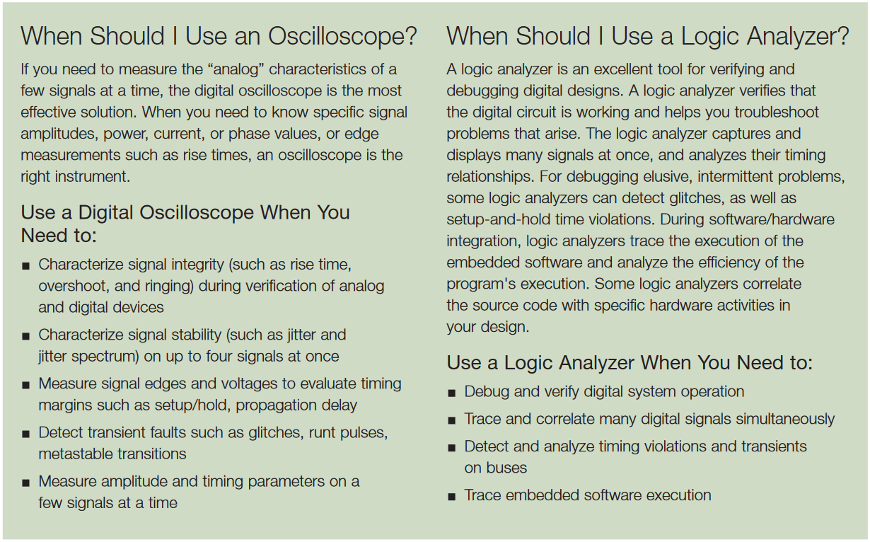
What is a Logic Analyzer?
Like so many electronic test and measurement tools, a logic analyzer is a solution to a particular class of problems. It is a versatile tool that can help you with digital hardware debug, design verification and embedded software debug. The logic analyzer is an indispensable tool for engineers who design digital circuits.
Logic analyzers are used for digital measurements involving numerous signals or challenging trigger requirements.
We will first look at the digital oscilloscope and the resulting evolution of the logic analyzer. Then you will be shown what comprises a basic logic analyzer. With this basic knowledge you’ll then learn what capabilities of a logic analyzer are important and why they play a major part in choosing the correct tool for your particular application.
Logic Analyzer vs. Oscilloscope: What's the Difference?
Logic analyzers evolved about the same time that the earliest commercial microprocessors came to market. Engineers designing systems based on these new devices soon discovered that debugging microprocessor designs required more inputs than oscilloscopes could offer.
Logic analyzers, with their multiple inputs, solved this problem. These instruments have steadily increased both their acquisition rates and channel counts to keep pace with rapid advancements in digital technology. The logic analyzer is a key tool for the development of digital systems.
There are similarities and differences between oscilloscopes and logic analyzers. To better understand how the two instruments address their respective applications, it is useful to take a comparative look at their individual capabilities.
The Digital Oscilloscope
The digital oscilloscope is the fundamental tool for generalpurpose signal viewing. Its high sample rate and bandwidth enables it to capture many data points over a span of time, providing measurements of signal transitions (edges), transient events, and small time increments.
While the oscilloscope is certainly capable of looking at the same digital signals as a logic analyzer, most oscilloscope users are concerned with analog measurements such as rise- and fall-times, peak amplitudes, and the elapsed time between edges.
A look at the waveform in Figure 1 illustrates the oscilloscope’s strengths. The waveform, though taken from a digital circuit, reveals the analog characteristics of the signal, all of which can have an effect on the signal’s ability to perform its function. Here, the oscilloscope has captured details revealing ringing, overshoot, rolloff in the rising edge, and other aberrations appearing periodically.
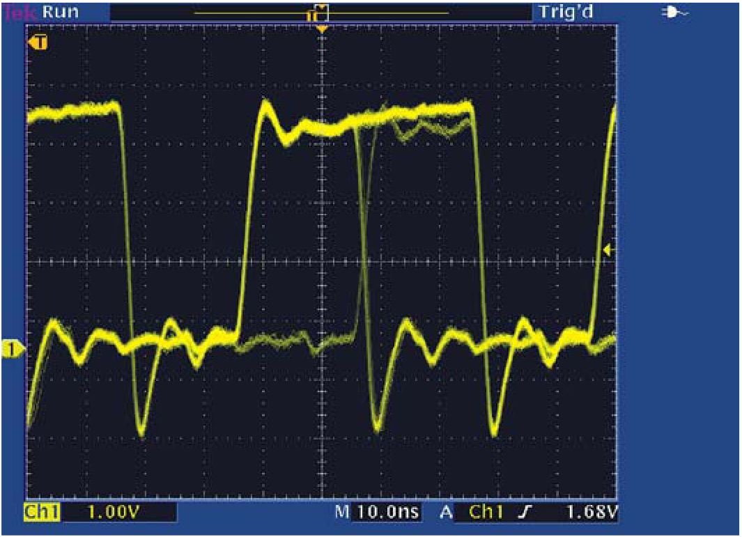
With the oscilloscope’s built-in tools such as cursors and automated measurements, it’s easy to track down the signal integrity problems that can impact your design. In addition, timing measurements such as propagation delay and setup-and-hold time are natural candidates for an oscilloscope. And of course, there are many purely analog signals – such as the output of a microphone or digital-to-analog converter – which must be viewed with an instrument that records analog details.
Oscilloscopes generally have up to four input channels. What happens when you need to measure five digital signals simultaneously – or a digital system with a 32-bit data bus and a 64-bit address bus? This points out the need for a tool with many more inputs – the logic analyzer.
The Logic Analyzer
The logic analyzer has different capabilities than the oscilloscope. The most obvious difference between the two instruments is the number of channels (inputs). Typical digital oscilloscopes have up to four signal inputs. Logic analyzers typically have between 34 and 136 channels. Each channel inputs one digital signal. Some complex system designs require thousands of input channels. Appropriately-scaled logic analyzers are available for those tasks as well.
A logic analyzer measures and analyzes signals differently than an oscilloscope. The logic analyzer doesn’t measure analog details. Instead, it detects logic threshold levels. When you connect a logic analyzer to a digital circuit, you’re only concerned with the logic state of the signal. A logic analyzer looks for just two logic levels, as shown in Figure 2.
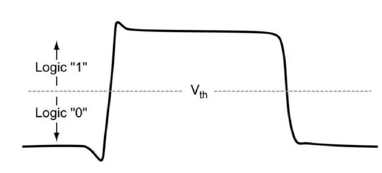
When the input is above the threshold voltage (V) the level is said to be “high” or “1;” conversely, the level below Vth is a “low” or “0.” When a logic analyzer samples input, it stores a “1” or a “0” depending on the level of the signal relative to the voltage threshold.
A logic analyzer’s waveform timing display is similar to that of a timing diagram found in a data sheet or produced by a simulator. All of the signals are time-correlated, so that setup-and-hold time, pulse width, extraneous or missing data can be viewed. In addition to their high channel count, logic analyzers offer important features that support digital design verification and debugging. Among these are:
- Sophisticated triggering that lets you specify the conditions under which the logic analyzer acquires data
- High-density probes and adapters that simplify connection to the system under test (SUT)
- Analysis capabilities that translate captured data into processor instructions and correlate it to source code
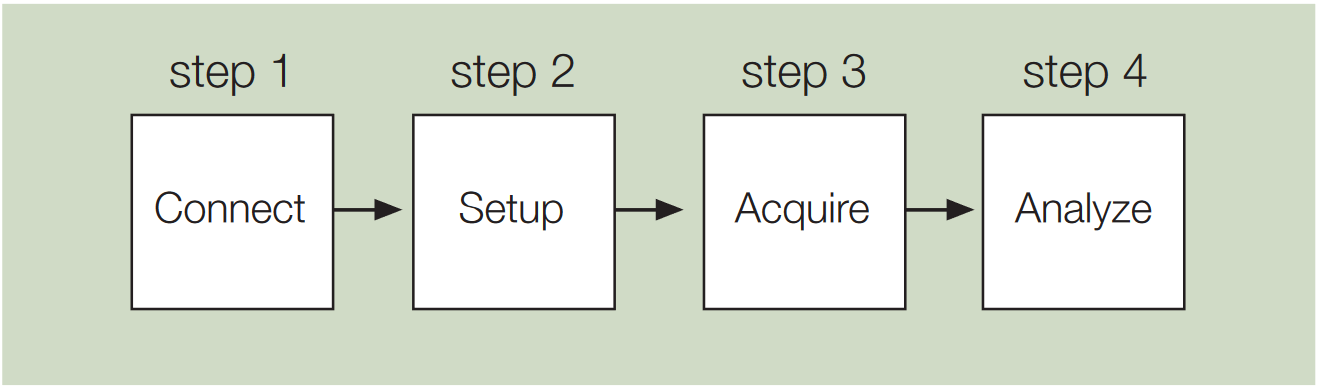
How to Use a Logic Analyzer
The logic analyzer connects to, acquires, and analyzes digital signals. There are four steps to using a logic analyzer as shown in Figure 3.
- Connect
- Setup
- Acquire
- Analyze
Connect to the System Under Test
Probe
The large number of signals that can be captured at one time by the logic analyzer is what sets it apart from the oscilloscope. The acquisition probes connect to the SUT. The probe’s internal comparator is where the input voltage is compared against the threshold voltage (Vth), and where the decision about the signal’s logic state (1 or 0) is made. The threshold value is set by the user, ranging from TTL levels to, CMOS, ECL, and user-definable.
Logic analyzer probes come in many physical forms:
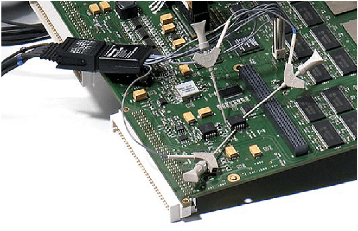
- General purpose probes with “flying lead sets” intended for point-by-point troubleshooting as shown in Figure 4.
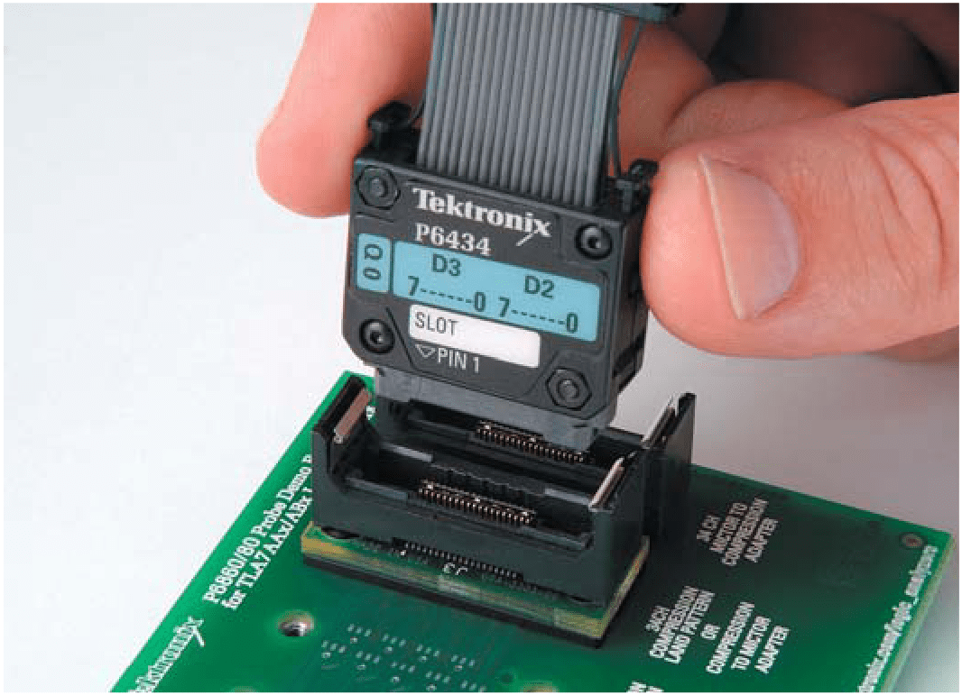
- High-density, multi-channel probes that require dedicated connectors on the circuit board as shown in Figure 5. The probes are capable of acquiring high-quality signals, and have a minimal impact on the SUT.
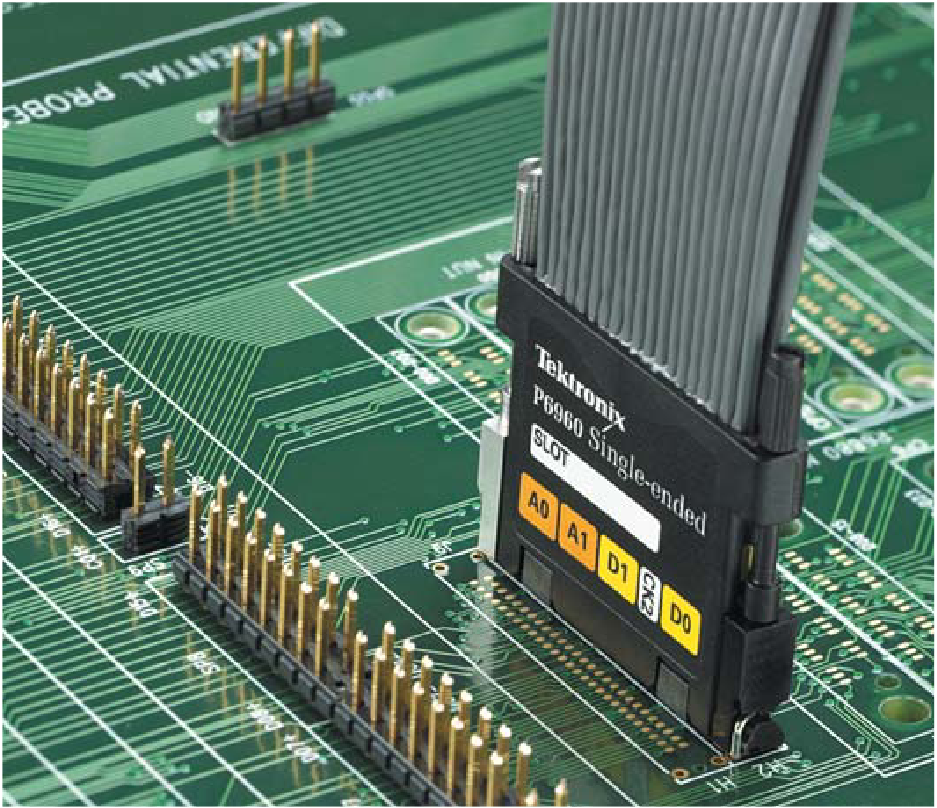
- High-density compression probes that use a connectorless probe attach as shown in Figure 6. This type of probe is recommended for those applications that require higher signal density or a connector-less probe attach mechanism for quick and reliable connections to your system under test.
The impedance of the logic analyzer’s probes (capacitance, resistance, and inductance) becomes part of the overall load on the circuit being tested. All probes exhibit loading characteristics. The logic analyzer probe should introduce minimal loading on the SUT, and provide an accurate signal to the logic analyzer.
Probe capacitance tends to “roll off” the edges of signal transitions, as shown in Figure 7. This roll off slows down the edge transition by an amount of time represented as “tD” in Figure 7. Why is this important? Because a slower edge crosses the logic threshold of the circuit later, introducing timing errors in the SUT. This is a problem that becomes more severe as clock rates increase.
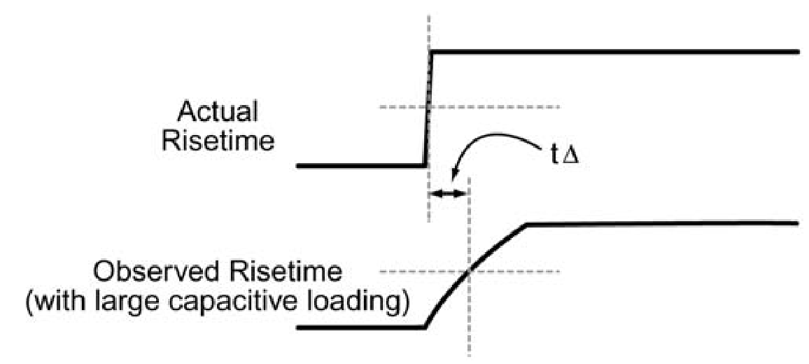
In high-speed systems, excessive probe capacitance can potentially prevent the SUT from working! It is always critical to choose a probe with the lowest possible total capacitance. It’s also important to note that probe clips and lead sets increase capacitive loading on the circuits that they are connected to. Use a properly compensated adapter whenever possible.
Set Up the Logic Analyzer
Set Up Clock Modes
Clock Mode Selection
Logic analyzers are designed to capture data from multi-pin devices and buses. The term “capture rate” refers to how often the inputs are sampled. It is the same function as the time base in an oscilloscope. Note that the terms “sample,” “acquire,” and “capture” are often used interchangeably when describing logic analyzer operations.
There are two types of data acquisition, or clock modes:
Timing acquisition captures signal timing information. In this mode, a clock internal to the logic analyzer is used to sample data. The faster that data is sampled, the higher will be the resolution of the measurement. There is no fixed timing relationship between the target device and the data acquired by the logic analyzer. This acquisition mode is primarily used when the timing relationship between SUT signals is of primary importance.
State acquisition is used to acquire the “state” of the SUT. A signal from the SUT defines the sample point (when and how often data will be acquired). The signal used to clock the acquisition may be the system clock, a control signal on the bus, or a signal that causes the SUT to change states. Data is sampled on the active edge and it represents the condition of the SUT when the logic signals are stable. The logic analyzer samples when, and only when, the chosen signals are valid. What transpires between clock events is not of interest here.
What determines which type of acquisition is used? The way you want to look at your data. If you want to capture a long, contiguous record of timing details, then timing acquisition, the internal (or asynchronous) clock, is right for the job.
Alternatively, you may want to acquire data exactly as the SUT sees it. In this case, you would choose state (synchronous) acquisition. With state acquisition, each successive state of the SUT is displayed sequentially in a Listing window. The external clock signal used for state acquisition may be any relevant signal.
Set Up Triggering
Triggering is another capability that differentiates the logic analyzer from an oscilloscope. Oscilloscopes have triggers, but they have relatively limited ability to respond to binary conditions. In contrast, a variety of logical (Boolean) conditions can be evaluated to determine when the logic analyzer triggers. The purpose of the trigger is to select which data is captured by the logic analyzer. The logic analyzer can track SUT logic states and trigger when a user-defined event occurs in the SUT.
When discussing logic analyzers, it’s important to understand the term “event.” It has several meanings. It may be a simple transition, intentional or otherwise, on a single signal line. If you are looking for a glitch, then that is the “event” of interest. An event may be the moment when a particular signal such as Increment or Enable becomes valid. Or an event may be the defined logical condition that results from a combination of signal transitions across a whole bus. Note that in all instances, though, the event is something that appears when signals change from one cycle to the next.
Many conditions can be used to trigger a logic analyzer.
For example, the logic analyzer can recognize a specific binary value on a bus or counter output. Other triggering choices include:
- Words: specific logic patterns defined in binary, hexadecimal, etc.
- Ranges: events that occur between a low and high value
- Counter: the user-programmed number of events tracked by a counter
- Signal: an external signal such as a system reset
- Glitches: pulses that occur between acquisitions
- Timer: the elapsed time between two events or the duration of a single event, tracked by a timer
- Analog: use an oscilloscope to trigger on an analog characteristic and to cross-trigger the logic analyzer
With all these trigger conditions available, it is possible to track down system errors using a broad search for state failures, then refining the search with increasingly explicit triggering conditions.
Acquire State and Timing Data
Simultaneous State and Timing
During hardware and software debug (system integration), it’s helpful to have correlated state and timing information.
A problem may initially be detected as an invalid state on the bus. This may be caused by a problem such as a setup and hold timing violation. If the logic analyzer cannot capture both timing and state data simultaneously, isolating the problem becomes difficult and time-consuming.
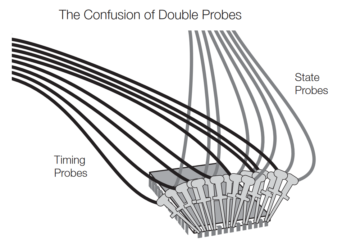
Some logic analyzers require connecting a separate timing probe to acquire the timing information and use separate acquisition hardware. These instruments require you to connect two types of probes to the SUT at once, as shown in Figure 8. One probe connects the SUT to a Timing module, while a second probe connects the same test points to a State module. This is known as “double-probing.” It’s an arrangement that can compromise the impedance environment of your signals. Using two probes at once will load down the signal, degrading the SUT’s rise and fall times, amplitude, and noise performance. Note that Figure 8 is a simplified illustration showing only a few representative connections. In an actual measurement, there might be four, eight, or more multi-conductor cables attached.
It is best to acquire timing and state data simultaneously, through the same probe at the same time, as shown in Figure 9. One connection, one setup, and one acquisition provide both timing and state data. This simplifies the mechanical connection of the probes and reduces problems.
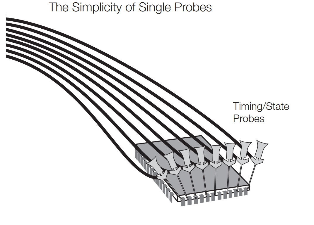
With simultaneous timing and state acquisition, the logic analyzer captures all the information needed to support both timing and state analysis. There is no second step, and therefore less chance of errors and mechanical damage that can occur with double probing. The single probe’s effect on the circuit is lower, ensuring more accurate measurements and less impact on the circuit’s operation.
The higher the timing resolution, the more details you can see and trigger on in your design, increasing your chance of finding problems.
Real-time Acquisition Memory
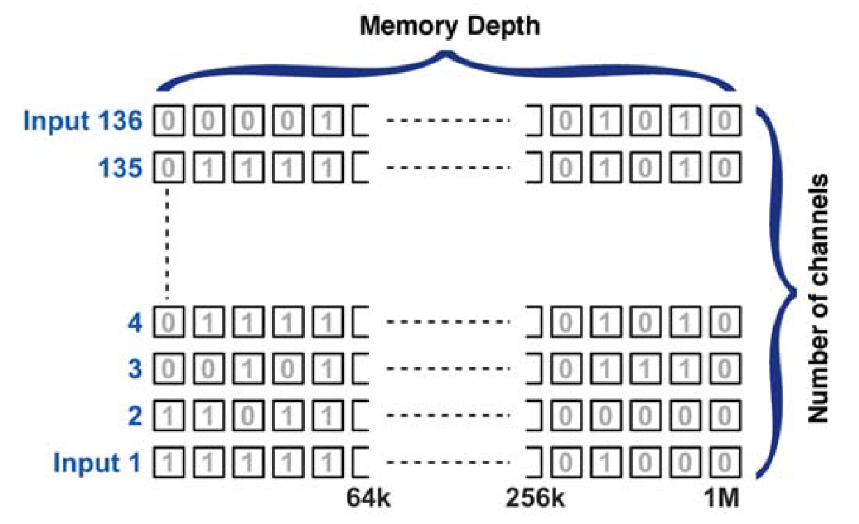
The logic analyzer’s probing, triggering, and clocking systems exist to deliver data to the real-time acquisition memory. This memory is the heart of the instrument – the destination for all of the sampled data from the SUT, and the source for all of the instrument’s analysis and display.
Logic analyzers have memory capable of storing data at the instrument’s sample rate. This memory can be envisioned as a matrix having channel width and memory depth, as shown in Figure 10.
How many signals do you need to capture and analyze?
Your logic analyzer’s channel count maps directly to the number of signals you want to capture. Digital system buses come in various widths, and there is often a need to probe other signals (clocks, enables, etc.) at the same time the full bus is being monitored. Be sure to consider all the buses and signals you will need to acquire simultaneously.
How much “time” do you need to acquire?
This determines the logic analyzer’s memory depth requirement, and is especially important for a timing acquisition. For a given memory capacity, the total acquisition time decreases as the sample rate increases. For example, the data stored in a 1M memory spans 1 second of time when the sample rate is 1 ms. The same 1M memory spans only 10 ms of time for an acquisition clock period of 10 ns.
Acquiring more samples (time) increases your chance of capturing both an error, and the fault that caused the error (see explanation which follows).
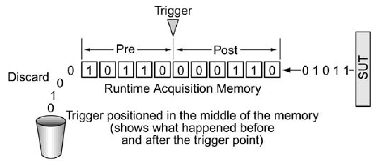
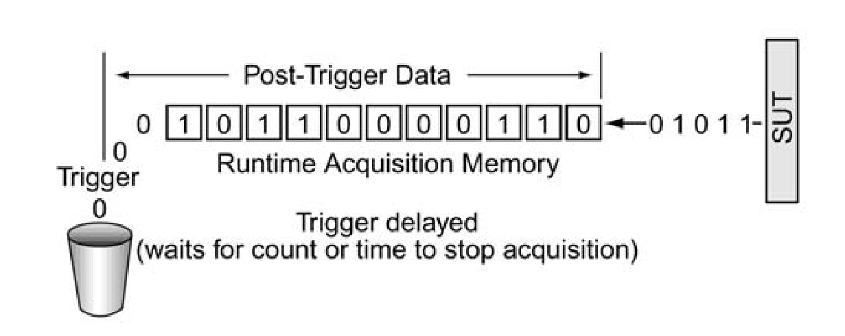
Logic analyzers continuously sample data, filling up the real-time acquisition memory, and discarding the overflow on a first-in, first-out basis as shown in Figure 11. Thus there is a constant flow of real-time data through the memory. When the trigger event occurs, the “halt” process begins, preserving the data in the memory.
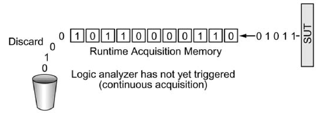
The placement of the trigger in the memory is flexible, allowing you to capture and examine events that occurred before, after, and around the trigger event. This is a valuable troubleshooting feature. If you trigger on a symptom – usually an error of some kind – you can set up the logic analyzer to store data preceding the trigger (pre-trigger data) and capture the fault that caused the symptom. You can also set the logic analyzer to store a certain amount of data after the trigger (post-trigger data) to see what subsequent affects the error might have had. Other combinations of trigger placement are available, as depicted in Figures 12 and 13.
With probing, clocking, and triggering set up, the logic analyzer is ready to run. The result will be a real-time acquisition memory full of data that can be used to analyze the behavior of your SUT in several different ways.
The logic analyzer’s main acquisition memory stores a long and comprehensive record of signal activity. Some of today’s logic analyzers can capture data at multi-gigahertz rates across hundreds of channels, accumulating the results in a long record length. This is ideal for a broad overview of long-term bus activity.
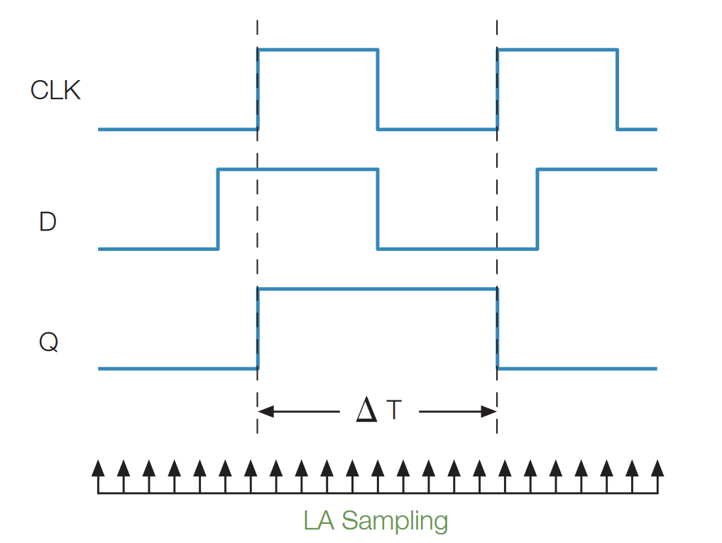
Each displayed signal transition is understood to have occurred somewhere within the sample interval defined by the active clock rate. The captured edge may have occurred just a few picoseconds after the preceding sample, or a few picoseconds before the subsequent sample, or anywhere in between. Thus the sample interval determines the resolution of the instrument. Evolving high-speed computing buses and communication devices are driving the need for better timing resolution in logic analyzers.
Tektronix MagniVu™ acquisition technology, a standard feature in the TLA Series, is the answer to this challenge. MagniVu acquisition relies on a high-speed buffer memory, that captures information at higher intervals around the trigger point. Here too, new samples constantly replace the oldest as the memory fills. Every channel has its own MagniVu buffer memory. MagniVu acquisition keeps a dynamic, high-resolution record of transitions and events that may be invisible at the resolution underlying the main memory acquisitions.
MagniVu acquisition is the key to the TLA Series’ industryleading ability to detect elusive timing errors such as narrow glitches and setup/hold violations that elude conventional logic analyzers. As shown in Figure 14 this high-resolution record can be viewed on the display in perfect alignment with the other timing waveforms in the main memory.
Integrated Analog-Digital Troubleshooting Tools
Designers attempting to track down digital errors must consider the analog domain as well. In today’s systems, with their fast edges and data rates, the analog characteristics underlying digital signals have an ever-increasing impact on system behavior—reliability and repeatability in particular.
Signal aberrations can arise from problems in the analog domain: impedance mismatches, transmission line effects, and more. Similarly, signal aberrations may be a by-product of digital issues such as setup and hold violations. There is a high degree of interaction among digital and analog signal effects.
The initial detection of an anomaly and its effect in the digital domain usually occurs in the logic analyzer. This is the tool that captures tens or even hundreds of channels at once, and for long spans of time; therefore it is the acquisition instrument most likely to be connected to the right signal at the right time.
Characterizing signal aberrations, once discovered, is the job of the real-time oscilloscope. It can acquire every glitch and transition in great detail, with precise amplitude and timing information. Tracking down these analog characteristics is often the shortest path to a solving a digital problem.
Efficient troubleshooting calls for tools and methods that can address both domains. Capturing the interaction between the two domains, and displaying it in both analog and digital forms, is the key to efficient troubleshooting.
Some modern solutions, notably the Tektronix TLA Series logic analyzers and the DPO Series oscilloscopes, include features to integrate the two platforms. The Tektronix iLinkTM toolset enables the logic analyzer and the oscilloscope to “collaborate,” sharing triggers and time-correlated displays.
The iLink™ toolset consists of several elements designed to speed problem detection and troubleshooting:
- iCapture™ multiplexing provides simultaneous digital and analog acquisition through a single logic analyzer probe.
- iView™ display delivers time-correlated, integrated logic analyzer and oscilloscope measurements on the logic analyzer display.
- iVerify™ analysis offers multi-channel bus analysis and validation testing using oscilloscope-generated eye diagrams.
Figure 15 depicts an iView screen display on a TLA Series logic analyzer. The signal appears in both its analog and digital forms as the TLA logic analyzer time correlates the integrated DPO oscilloscope trace.
Analyze and Display Results
The data stored in the real-time acquisition memory can be used in a variety of display and analysis modes. Once the information is stored within the system, it can be viewed in formats ranging from timing waveforms to instruction mnemonics correlated to source code.
Waveform Display
The waveform display is a multi-channel detailed view that lets you see the time relationship of all the captured signals, much like the display of an oscilloscope. Figure 16 is a simplified waveform display. In this illustration, sample clock marks have been added to show the points at which samples were taken.
The waveform display is commonly used in timing analysis, and it is ideal for:
- Diagnosing timing problems in SUT hardware
- Verifying correct hardware operation by comparing the recorded results with simulator output or data sheet timing diagrams
- Measuring hardware timing-related characteristics:
– Race conditions
– Propagation delays
– Absence or presence of pulses - Analyzing glitches
Listing Display
The listing display provides state information in user-selectable alphanumeric form. The data values in the listing are developed from samples captured from an entire bus and can be represented in hexadecimal or other formats.
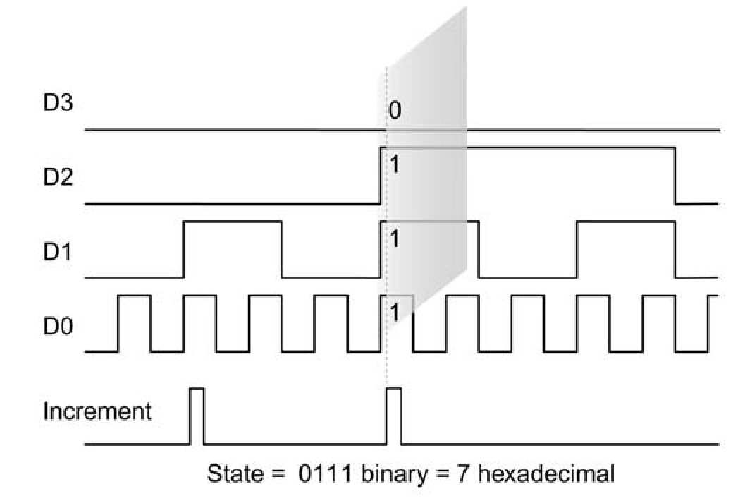
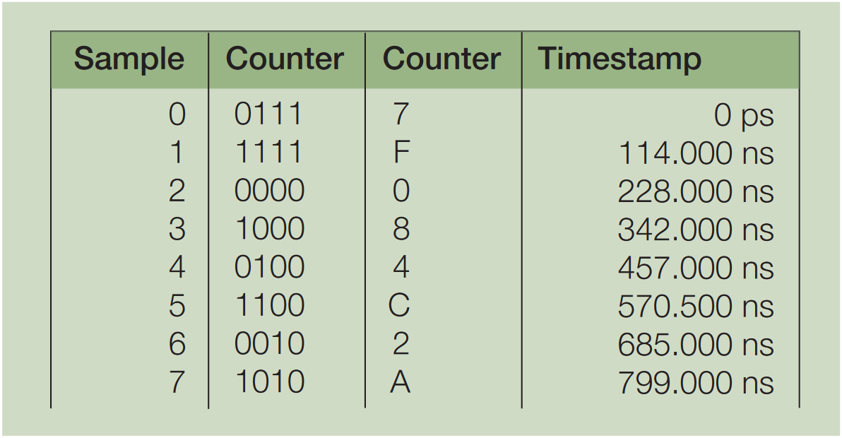
Imagine taking a vertical “slice” through all the waveforms on a bus, as shown in Figure 17. The slice through the fourbit bus represents a sample that is stored in the real-time acquisition memory. As Figure 17 shows, the numbers in the shaded slice are what the logic analyzer would display typically in hexadecimal form.
The intent of the listing display is to show the state of the SUT. The listing display in Figure 18 lets you see the information flow exactly as the SUT sees it – a stream of data words.
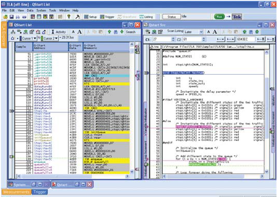
State data is displayed in several formats. The real-time instruction trace disassembles every bus transaction and determines exactly which instructions were read across the bus. It places the appropriate instruction mnemonic, along with its associated address, on the logic analyzer display. Figure 19 is an example of a real-time instruction trace display.
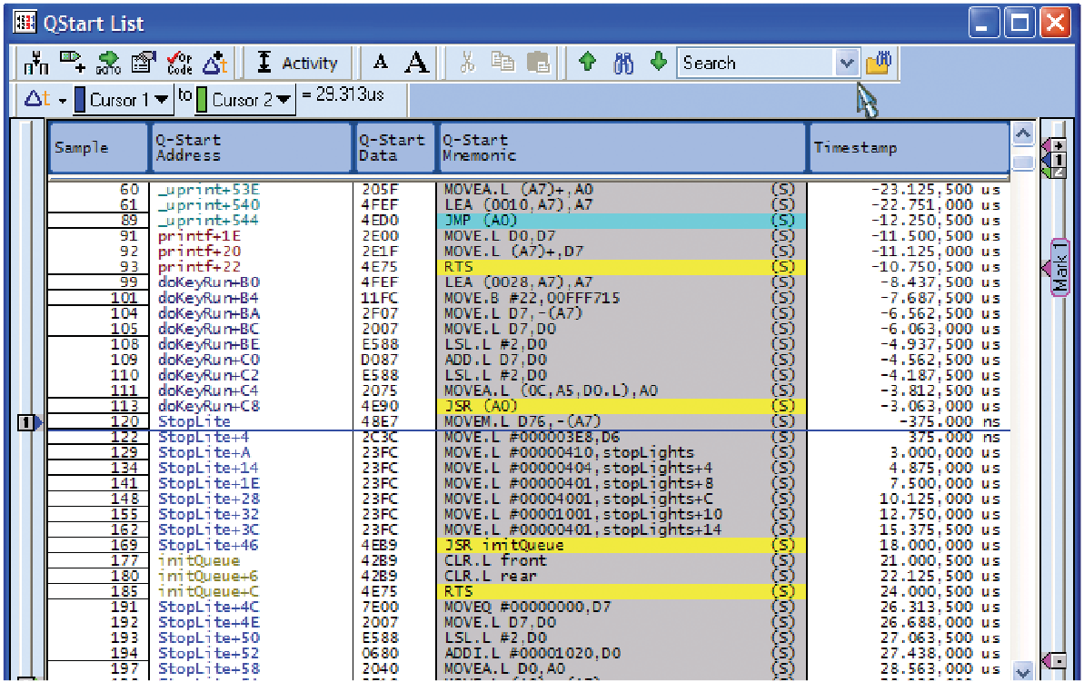
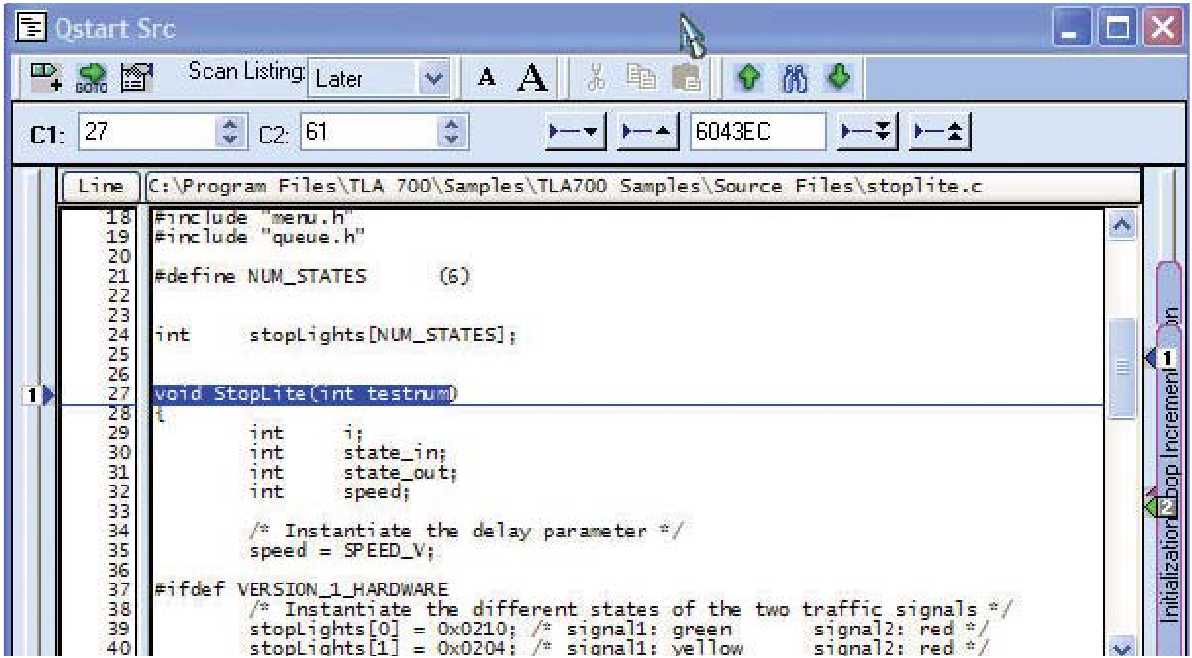
An additional display, the source code debug display, makes your debug work more efficient by correlating the source code to the instruction trace history. It provides instant visibility of what’s actually going on when an instruction executes. Figure 20 is a source code display correlated to the Figure 19 real-time instruction trace.
With the aid of processor-specific support packages, state analysis data can be displayed in mnemonic form. This makes it easier to debug software problems in the SUT. Armed with this knowledge, you can go to a lower-level state display (such as a hexadecimal display) or to a timing diagram display to track down the error’s origin.
State analysis applications include:
- Parametric and margin analysis (e.g., setup & hold values)
- Detecting setup-and-hold timing violations
- Hardware/software integration and debug
- State machine debug
- System optimization
- Following data through a complete design
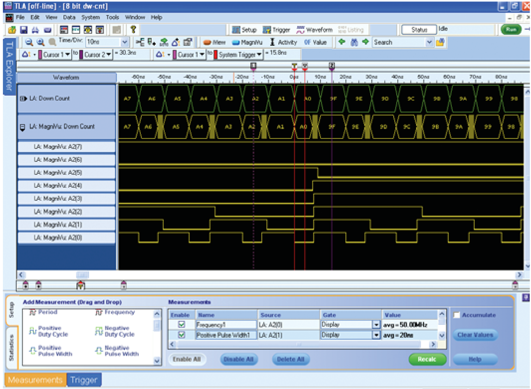
Automated Measurements
Drag and drop automated measurements provide the ability to perform sophisticated measurements on logic analyzer acquisition data. A broad selection of oscillo-scope-like measurements are available, including frequency, period, pulse width, duty cycle, and edge count. The automated measurements deliver fast and thorough results by quickly providing measurement results on very large sample sizes. Performing a measurement is simple: click on a measurement icon selected from a group of related icons appearing in a tabbed pane; drag the icon to a waveform trace in the main window; and release-“drop”-the click. The logic analyzer sets up the measurement, performs any necessary analysis steps (for example, calculating the pulse width), and displays the result as seen in Figure 21. Note that these steps are fully automated, allowing you to dispose of time consuming manual measurement methods previously used.
Key Logic Analyzer Specifications That Matter
The logic analyzer has a number of quantitative indicators of its performance and effectiveness, with several of these related to its sample rate. This is the measurement frequency axis that is analogous to the bandwidth of a digital phosphor oscilloscope (DPO). Certain probing and triggering terms will also be familiar to the DPO user, but there are many attributes that are unique to the logic analyzer’s digital domain.
Because the logic analyzer is not attempting to capture and reconstruct an analog signal, issues like channel count and synchronization (clock) modes are critical while analog factors such as vertical accuracy are secondary.
The following list of performance terms and considerations references the current Tektronix TLA Series logic analyzers, an industry-leading solution that meets the needs of the most demanding digital design applications.
Timing Acquisition Rate
The logic analyzer’s most basic mission is to produce a timing diagram based on the data it has acquired. If the DUT is functioning correctly and the acquisition is properly set up, the logic analyzer’s timing display will be virtually identical to the timing diagram from the design simulator or data book.
But that depends on the resolution of the logic analyzer— in effect, its sample rate. Timing acquisition is asynchronous; that is, the sample clock is free-running relative to the input signal. The higher the sample rate, the more likely it is that a sample will accurately detect the timing of an event such as a transition.
For example, a TLA Series logic analyzer with a sample frequency of 50 GHz, would equate to 20 ps resolution. Therefore the timing display reflects edge placements within 20 ps of the actual edge, worst case.
State Acquisition Rate
State acquisition is synchronous. It depends on an external trigger from the DUT to clock the acquisitions. State acquisition is designed to assist engineers in tracing the data flow and program execution of processors and buses. Logic analyzers, such as the TLA Series, may offer state acquisition frequencies of 1.4 GHz, with a setup/hold window of 180 ps across all channels to ensure accurate data capture.
Note that this frequency is relevant to the bus and I/O transactions the logic analyzer will monitor, not the DUT’s internal clock rate. Though the device’s internal rate may be in the multi-gigahertz range, its communication with buses and other devices is on the same order as the logic analyzer’s state acquisition frequency.
MagniVu Acquisition Rate
MagniVu acquisition is applicable to either the timing or state acquisition modes. MagniVu acquisition provides higher sampling resolution on all channels to more easily find difficult problems by accumulating additional samples around the trigger point. Additional capabilities include adjustable MagniVu sample rates, movable trigger positions, and a separate MagniVu trigger action that can be triggered independent of the main trigger.
Record Length
Record length is another key logic analyzer specification. A logic analyzer capable of storing more “time” in the form of sampled data is useful because the symptom that triggers an acquisition may occur well after its cause. With a longer record length, it is often possible to capture and view both, greatly simplifying the troubleshooting process.
TLA Series logic analyzers can be configured with various record lengths. It is also possible to concatenate the memory from up to four channels to quadruple the available depth. This provides a means to build massive record lengths when needed, or to get the performance of a long record length from a smaller, lower-cost configuration.
Channel Count and Modularity
The logic analyzer’s channel count is the basis of its support for wide buses and/or multiple test points through-out a system. Channel count also is important when reconfiguring the instrument’s record length: two or four channels are required in order to double or quadruple the record length, respectively.
With today’s trend toward high-speed serial buses, the channel count issue is as critical as ever. A 32-bit serial data packet, for example, must be distributed to not one, but 32 logic analyzer channels. In other words, the transition from parallel to serial architectures has not affected the need for channel count.
Standalone TLA Series logic analyzers can be configured with a wide range of channel counts. The modular TLA Series logic analyzers can accommodate a variety of acquisition modules, and can be connected together for even higher channel counts. Ultimately the system can accommodate thousands of acquisition channels. The modular TLA Series architecture is uniquely able to maintain synchronization and low latency from module to module, even if the modules are in different mainframes.
Triggering
Triggering flexibility is the key to fast, efficient detection of unseen problems. In a logic analyzer, triggering is about setting conditions that, when met, will capture the acquisition and display the result. The fact that the acquisition has stopped is proof that the condition occurred (unless a timeout exception is specified).
Today, triggering setup is simplified by drag-and-drop triggering for easier setup of common trigger types. These triggers spare the user from the need to devise elaborate trigger configurations for everyday timing problems. As the application examples later in this document will demonstrate, logic analyzers also allow powerful specialization of these triggers to address more complex problems.
Logic analyzers also provide multiple trigger states, word recognizers, edge/transition recognizers, range recognizers, timer/counters, and a snapshot recognizer in addition to the glitch and setup/hold triggers.
Probing
As circuit densities and speeds increase dramatically with each new generation of electronic products, probing solutions become an increasingly important component of the overall logic analyzer solution. Probes must offer channel densities that match the target devices while providing positive connections and preserving the signal quality.
The D-Max™ technology underlying Tektronix’ connectorless logic analyzer probes is one innovative approach to these challenges. They provide a durable, reliable mechanical and electrical connection between the probe and the circuit board. Their industry-leading input capacitance minimizes the probes’ loading effects on the signal. These compression probes are designed to mate with simple landing pads on the circuit board, conserving precious board real estate and minimizing layout complexity and cost.
Logic Analyzer Measurement Examples
The following series of examples will illustrate several common measurement problems and their solutions.
The explanations are simplified to focus on some basic logic analyzer acquisition techniques and the display of the resulting data.
Certain setup steps and configuration details have been omitted for the sake of brevity. For additional details, please refer to your instrument documentation, application notes, and other technical information.
Making General Purpose Timing Measurements
Ensuring the proper timing relationships between critical signals in a digital system is an essential step in the validation process. A wide range of timing parameters and signal must be evaluated: propagation delay, pulse width, setup and hold characteristics, signal skew, and more.
Efficient timing measurements call for a tool that can provide high-resolution acquisition across numerous channels with minimal loading on the circuit being measured. The tool must have flexible triggering capabilities that help the designer to quickly locate problems by defining explicit trigger conditions. In addition, the tool must provide display and analysis capabilities that simplify the interpretation of long records.
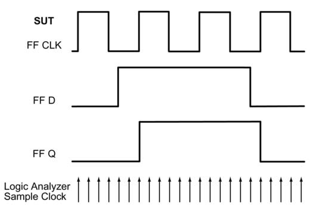
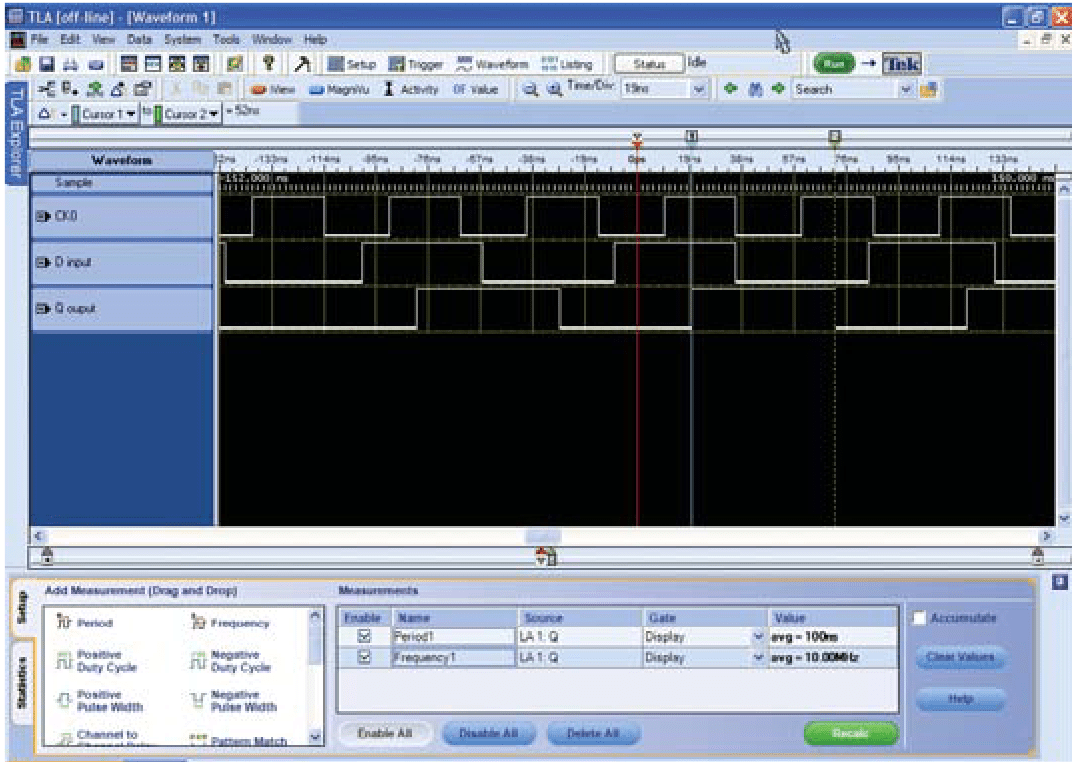
Timing measurements are commonly required when validating a new digital design. The following example demonstrates a timing measurement on a “D” flip-flop with the connections shown in Figure 22. This example is based on the features of the Tektronix TLA Series logic analyzers. In the real world, such a measurement might simultaneously acquire hundreds or even thousands of signals. But the principle is the same in either case, and as the example proves, timing measurements are fast, easy, and accurate.
- Set up the triggering and clocking. This example uses the “IF Anything, THEN Trigger” setup and Internal (asynchronous) clocking. There is also a setup step, beyond the scope of this discussion, to name and map the signals to specific logic analyzer channels.
- After executing a “Run” operation to acquire the signal data, use the Horizontal Position control or the memory scroll bar to position the on-screen data such that the trigger indicator (marked with a “T”) is in view.
- Place the mouse pointer on the leading edge of the Q signal and right-click the mouse. Selecting “Move cursor 1 here” from the resulting menu will move the first measurement cursor to this location. You can then “snap” the cursor to the leading edge using the drag-and-drop feature. This becomes the beginning of the timespan that will be measured.
- Place the mouse cursor on the trailing edge of the Q signal. Right-click and select “Move cursor 2 here” to place the cursor. Again, you can use the “snap” cursor feature to more easily align the cursor to the edge. This becomes the end of the measured timespan.
- Since the Y axis of the display denotes time, the subtractive difference between Cursor 2 and Cursor 1 is the time measurement. The result of 52 ns appears in the “Delta Time” readout on the display. The resolution of the measurement depends on the sample rate; in Figure 23 it is 2 ns as indicated by the ticks on the Sample track. Notice that the "Delta Time" measurement can not have a resolution greater than the sample rate.
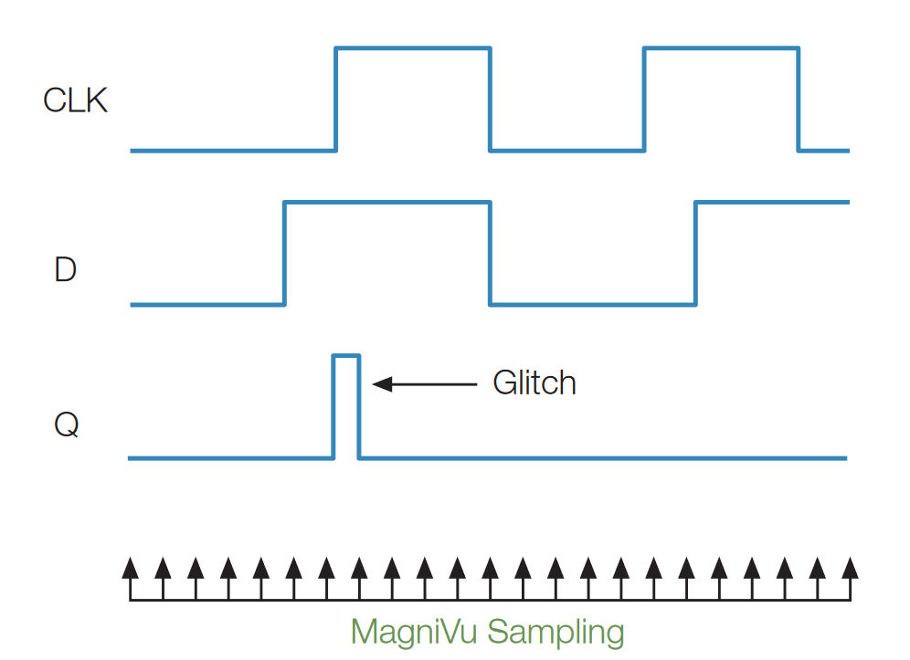
Detecting and Displaying Intermittent Glitches
Glitches are a constant annoyance for digital system designers. These erratic pulses are intermittent, and they may be irregular in amplitude and duration. They are inevitably difficult to detect and capture, yet the effects of an unpredictable glitch can disable a system. For example, a logic element can easily misinterpret a glitch as a clock pulse. This in turn might send data across the bus prematurely, creating errors that ripple through the entire system.
Any number of conditions can cause glitches: crosstalk, inductive coupling, race conditions, timing violations, and more. Glitches can elude conventional logic analyzer timing measurements simply because they are so brief in duration. A glitch can easily appear, then vanish in the time between two logic analyzer acquisitions.
Only a logic analyzer with very high timing resolution (that is, a high clock frequency when running in its asynchronous mode) can hope to capture these brief events. Ideally, the logic analyzer will automatically highlight the glitch and the channel.
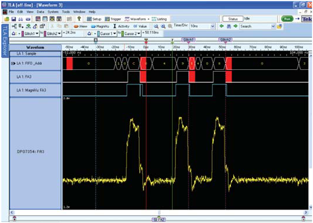
The following example illustrates the process of capturing a narrow glitch using a TLA Series logic analyzer. The device under test (DUT) is again a “D” flip-flop with the signal timing shown in Figure 24. The MagniVu timing resolution is used to detect and display the glitch with great precision.
Again, this example is not meant to be a detailed tutorial; some steps have been omitted for consistency with the level of this primer.
- In previous trigger setups, we have acquired waveforms in our waveform window. Capturing a glitch is easy with drag-and-drop triggering.
- Click the “Trigger” tab at the bottom of the screen.
- Click the Glitch trigger option in the basket, drag-anddrop it onto the bus waveform.
- Now, click the Run button. Glitches on those buses will then be captured and displayed on the waveform window.
The acquisition is shown in Figure 25. This screen includes several channels which have been added (by means of a separate setup step that does not require a second acquisition) to display the contents of the high-resolution On the Q output waveform trace, note the red flag to the left of (earlier than) the trigger indicator. This announces that a glitch has been detected somewhere in the red area between the trigger sample point and the immediately previous data sample point. The Q output’s MagniVu channel (bottom trace) reveals exactly where the glitch occurred. At this point, the timing of the glitch is known and the instrument’s zoom and cursor features can be used to measure the pulse width.
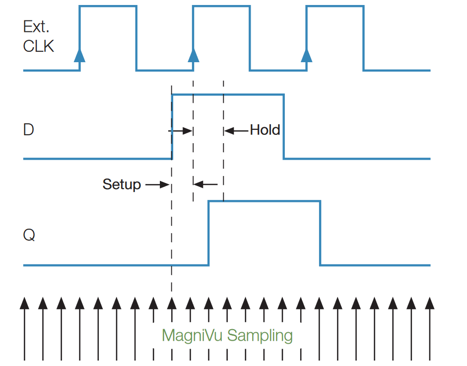
Capturing Setup or Hold Violations
Setup time is defined as the minimum time that input data must be valid and stable prior to the clock edge (see Figure 26) that shifts it into the device. Hold time is the minimum time that the data must be valid and stable after the clock edge occurs.
Digital device manufacturers specify Setup and Hold parameters and engineers must take great care to ensure that their designs do not violate the specifications. But today’s tighter tolerances and the widespread use of faster parts to drive more throughput is making setup and hold violations ever more common.
These violations can cause the device output to become unstable (a condition known as metastability) and potentially cause unexpected glitches and other errors. Designers need to examine their circuits closely to determine whether violations of the design rules are causing setup and hold problems.
In recent years, both Setup and Hold requirements have narrowed to the point where it is difficult for most conventional general-purpose logic analyzers to detect and capture the events. The only real answer is a logic analyzer with sub-nanosecond sampling resolution.
The Tektronix TLA Series logic analyzers with their MagniVu acquisition features are a proven solution for Setup and Hold measurements.
The following example introduces synchronous acquisition mode, which relies on an external clock signal to drive the sampling. Irrespective of the mode, the MagniVu feature is always available and provides a buffer of high-resolution sample data around the trigger point. Once again the DUT is a “D” flip-flop with a single output but the example is equally applicable to a device with hundreds of outputs.
Using a MagniVu acquisition to view the data gives us the highest possible timing resolution. It should be noted that for this tutorial we have constructed a data window that only includes MagniVu acquisitions. Since you will be triggering on a setup or hold violation, the MagniVu feature can give you the best possible timing resolution around the violation.
In this example the DUT itself provides the External Clock signal that controls the synchronous acquisitions. The logic analyzer drag-and-drop trigger capability can be used to create a Setup and Hold trigger. Unique to this mode is the ability to easily define the explicit Setup and Hold timing violation parameters, as shown in Figure 27. Additional submenus in the setup window are available to refine other aspects of the signal definition, including logic conditions and positive- or negative-going terms.
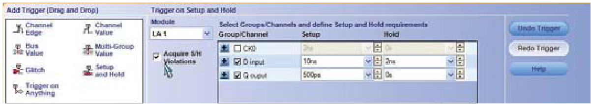
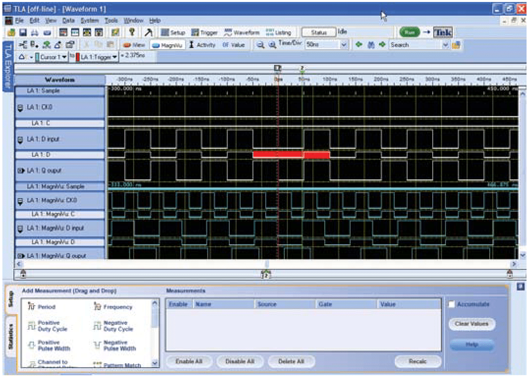
When the test runs, the logic analyzer actually evaluates every rising edge of the clock for a setup or hold violation. It monitors millions of events and captures only those that fail the setup or hold requirements. The resulting display is shown in Figure 28. Here the setup time is 2.375 ns, far less than the defined limit of 10 ns.
Applying Transitional Storage to Maximize Usable Record Length
Sometimes the device under test puts out a signal that consists of occasional clusters of events separated by long intervals of inactivity. For example, certain types of radar systems drive their internal D/A converters with widely separated bursts of data.
This is a problem when using conventional logic analyzer acquisition and storage techniques. The instrument uses one memory location for every sample interval, a method appropriately named “Store All.” This can quickly fill the acquisition memory with unchanging data, consuming valuable capacity needed to capture the actual data of interest—the bursts of the active signal.
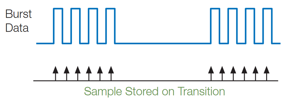
An approach known as “Transitional Storage” solves the problem by storing data only when transitions occur. Figure 29 depicts the concept. The logic analyzer samples when, and only when, the data changes. Bursts that are seconds, minutes, hours, or even days apart can be captured with the full resolution of the logic analyzer’s main sample memory. The instrument waits out the long dormant periods. Note that these long spans of inactivity aren’t “ignored.” On the contrary, they are constantly monitored. But they are not recorded.
The following example illustrates the solution as implemented with a TLA Series logic analyzer. The versatile IF/THEN triggering algorithm is again the best tool for distinguishing the unique circumstances that prompt the transitional storage.
The TLA Series interface provides a pull-down Storage menu to select “Transitional” rather than “All” events. This brings up a menu from which the “IF Channel Burst=High THEN Trigger” mode can be invoked.
Running the test with these conditions specified will produce a screen display similar to the one shown in Figure 30. Here, the burst contains nine groups of eight pulses, 22 ns in width, with the groups separated by quiescent intervals of 428 ns. Transitional storage has allowed the instrument to capture all sixteen of these burst groups, including the seven remaining off screen, while consuming only 256 of record length. The time window represents almost 3.8 milliseconds of acquisition time, where the groups repeat every 2 milliseconds.
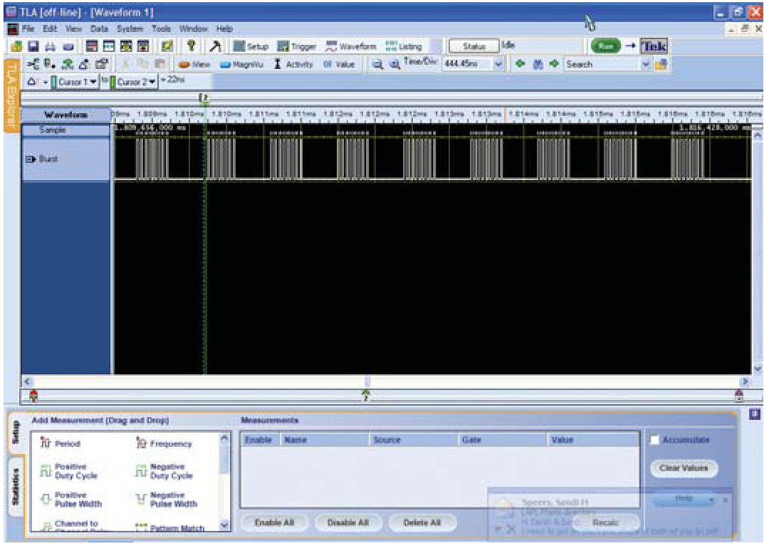
In contrast, the Store All acquisition mode would capture only one of the burst groups using two thousand times the memory space at 512K. The allocated memory would fill up in about 1 microsecond, with much of the space being occupied by “blank” inactive cycles. Transitional storage makes it possible to gather much more usable information every time you run an acquisition.
Logic Analyzers Application Examples
The following section provides an overview of the measurement requirements and considerations that need to be considered in some of today’s key applications.
FPGA
The phenomenal growth in design size and complexity makes the process of design verification a critical bottleneck for today’s FPGA systems. Limited access to internal signals, advanced FPGA packages, and printed circuit board (PCB) electrical noise are all contribute to making FPGA debug and verification the most difficult process of the design cycle. You can easily spend more than 50% of your design cycle time debugging and verifying your design. To help you with the process of design debugging and verification, new tools are required to help debug your design while it is running at full speed on your FPGA.
One of the key choices that needs to be made in the Design Phase is deciding which FPGA debug methodology to use. Ideally, you want a methodology that is portable to all of your FPGA designs, provides you insight into both your FPGA operation and your system operation, and gives you the power to pinpoint and analyze difficult problems. There are really two basic in-circuit FPGA debug methodologies: the first is the use of an embedded logic analyzer and the second is the use of an external logic analyzer. The choice of which methodology to use depends on the debug needs of your project.
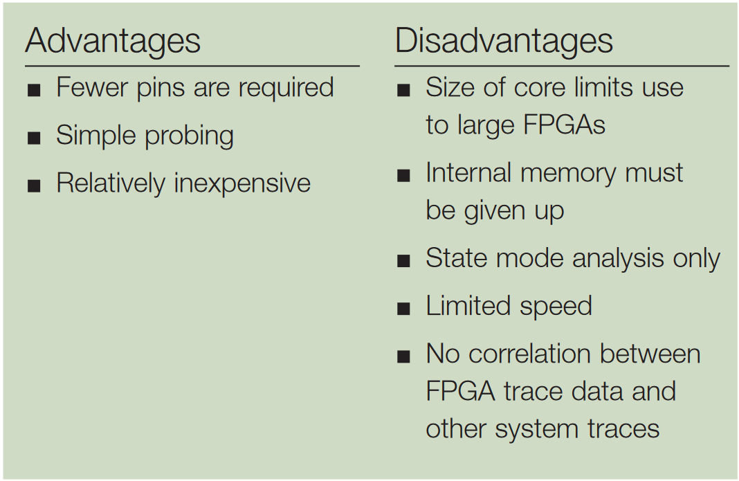
Each of the FPGA vendors offers an embedded logic analyzer core. These intellectual property blocks are inserted into your FPGA design and provide both triggering capability and storage capability. It is important to note that FPGA logic resources are used to implement the trigger circuit and FPGA memory blocks are used to implement the storage capability. JTAG is typically used to configure the operation of the core and then is used to pass the captured data to a PC for viewing. Because the embedded logic analyzer uses internal FPGA resources, they are most often used with larger FPGAs that can better absorb the overhead of the core. As with any debug methodology, the embedded logic analyzer has some tradeoffs that you should be aware of:
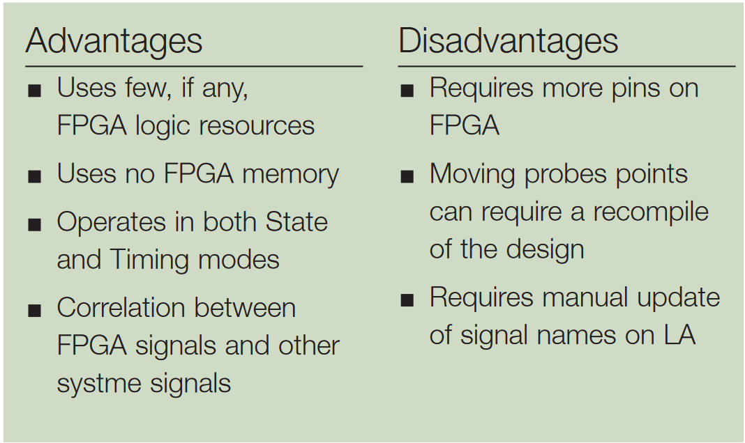
Because of the limitations of the embedded logic analyzer methodology, many FPGA designers have adopted a methodology that uses the flexibility of the FPGA and the power of an external logic analyzer such as the TLA Series of logic analyzers. In this methodology, internal signals of interest are routed to pins of the FPGA, which are then connected to an external logic analyzer. This approach offers very deep memory, which is useful when debugging problems where the symptom and the actual cause are separated by a large amount of time. It also offers the ability to correlate the internal FPGA signals with other activity in the system. As with the embedded logic analyzer methodology, there are trade-offs to consider.
Both methodologies can be useful depending on your situation. The challenge is to determine which approach is appropriate for your design. Ask yourself the following questions. What are the anticipated problems? If you think they will be isolated to functional problems within the FPGA, the use of an embedded logic analyzer may be all the debug capability that you need. If, however, you anticipate larger debug problems that may require you to verify timing margins, correlate internal FPGA activity with other activity on your board, or more powerful triggering capability to isolate the problem, the use of an external logic analyzer is more suited to your debug needs.
Let’s look at the external logic analyzer approach in some more detail. In essence, this method makes use of the P in FPGA to reprogram the device as needed to route the internal signals of interest to what is typically a small number of pins. This is a very useful approach but it does have limitations. Every time you need to look at a different set of internal signals, you may need to change your design (either at the RTL-level or using an FPGA editor tool) to route the desired set of signals to the debug pins. This is not only time- consuming but if it requires a recompile of your design, it will take even more time and it can potentially hide the problem by changing the timing of your design. There are typically a small number of debug pins and the 1:1 relationship between internal signals and debug pins limits visibility and insight into the design.
To overcome these limitations, a new method of FPGA debug has been created that delivers all of the advantages of the external logic analyzer approach while removing its primary limitations. First Silicon Solution’s FPGAView software package, when used with a Tektronix TLA Series logic analyzer, provides a complete solution for debugging your Altera or Xilinx FPGA and the surrounding hardware.
The combination of FPGAView and a TLA logic analyzer allows you to see inside of your FPGA design and correlate internal signals with external signals. Productivity is increased because the time-consuming process of recompiling your design is eliminated and you have access to multiple internal signals per debug pin. In addition, FPGAView can handle multiple test cores in a single device. This is useful for when you need to monitor different clock domains inside your FPGA. It can also handle multiple FPGAs on a JTAG chain.
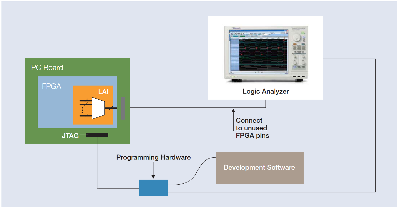
As shown in Figure 31, the complete solution consists of four pieces. In this example the first piece is a test multiplexer provided by Altera in their Quartus® II software suite. This test multiplexer is available to all Quartus II software users.
The second piece is the FPGAView software package that allows the user to control the Test Mux and integrates the other pieces into a powerful tool. The third piece is a TLA Series logic analyzer to acquire and analyze the data. And the final piece is a JTAG programming cable used to control the test multiplexer inside your FPGA.
The combination of FPGAView and a TLA Series logic analyzer can simplify many of your debug tasks with respect to FPGAs.
This tool set allows you to see inside of your FPGA design and correlate internal signals with external signals. Productivity is increased because the time-consuming process of recompiling your design is eliminated and you have access to multiple internal signals per pin.
Memory
Dynamic Random Access Memory has evolved over time driven by faster, larger and lower powered memory requirements and smaller physical sizes. The first step went to Synchronous Dynamic RAM which provided a clock edge to synchronize its operation with the memory controller. Then the data rate was increased by using Double Data Rate (DDR). And then to overcome signal integrity issues, DDR2 SDRAM and DDR3 SDRAM evolved to go faster.
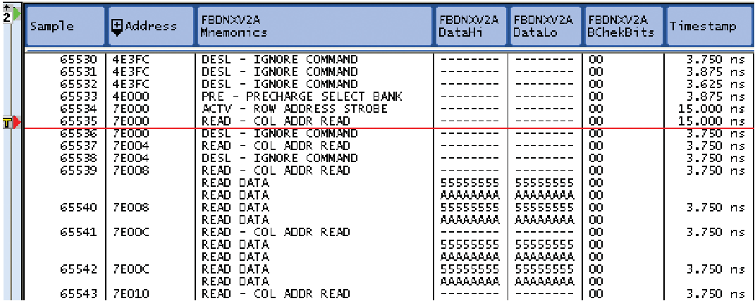
To keep pace with the more complex and shorter design cycles, memory designers need a variety of different test equipment to check out their design. If you are looking at impedance and trace length you will use sampling oscilloscopes. If you are looking at the electrical signals, from power to signal integrity to clocks, jitter and so forth, you will use digital phosphor oscilloscopes. If you are looking at the commands and protocols, you will use logic analyzers to verify your memory system’s operation, as shown in Figure 32.
Logic analyzer memory supports enhance the operation of the logic analyzer by configuring the logic analyzer setup, providing custom clocking for memory acquisition, memory data analysis software, mnemonics listing, and may include memory probing hardware. Nexus Technology, Inc. is a Tektronix Embedded Systems Tools Partner that provides logic analyzer memory supports and complementary products for Tektronix logic analyzers and oscilloscopes. Tektronix also distributes selected Nexus Technology products.
Signal Integrity
Direct signal observations and measurements are the only way to discover the causes of signal integrity-related problems. As always, choosing the right tool will simplify your job. For the most part, signal integrity measurements are carried out by the same familiar instruments found in almost any electronic engineering lab. These instruments include the logic analyzer and the oscilloscope. Probes and application software round out the basic toolkit. In addition, signal sources can be used to provide distorted signals for stress testing and evaluation of new devices and systems.
When it comes to setting up a signal integrity measurement system the key considerations center around:
- Probing
- Bandwidth & step response
- Timing resolution
- Record length
- Triggering
- Integration
When troubleshooting digital signal integrity problems, especially in complex systems with numerous buses, inputs and outputs, the logic analyzer is the first line of defense.
This instrument has the high channel count, deep memory, and advanced triggering to acquire digital information from many test points, and then display the information coherently. Because it is a truly digital instrument, the logic analyzer detects threshold crossings on the signals it is monitoring, and then displays the logic signals as seen by logic ICs. The resulting timing waveforms are clear and understandable, and can easily be compared with expected data to confirm that things are working correctly. These timing waveforms are usually the starting point in the search for signal problems that compromise signal integrity. These results can be further interpreted with the help of disassemblers and processor support packages, which allow the logic analyzer to correlate the real-time software trace (correlated to source code) with the low-level hardware activity, as shown in Figure 33.
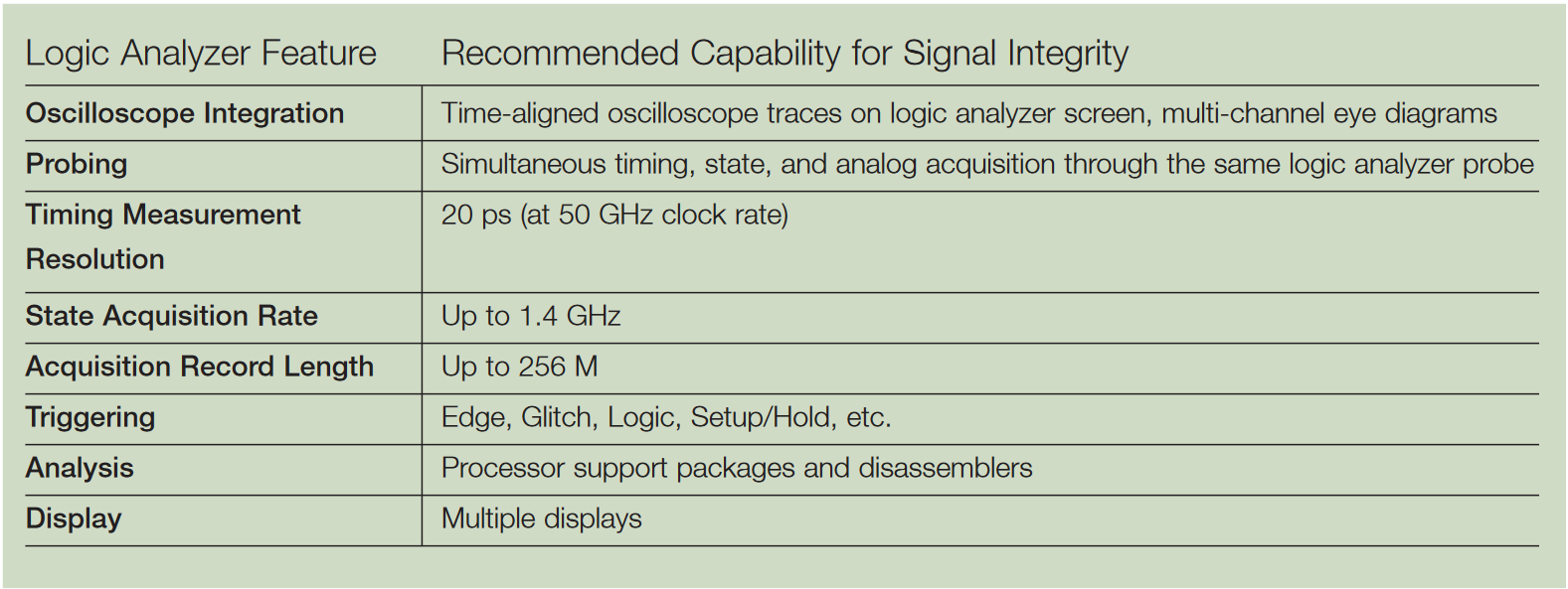
However not every logic analyzer qualifies for signal integrity analysis at today’s extremely high (and increasing!) digital data rates. Figure 34 provides some specification guidelines that should be considered when choosing a logic analyzer for advanced signal integrity troubleshooting. With all the emphasis on sample rates and memory capacities, it is easy to overlook the triggering features in a logic analyzer. Yet triggers are often the quickest way to find a problem. After all, if a logic analyzer triggers on an error, it is proof that an error has occurred. Most current logic analyzers include triggers that detect certain events that compromise signal integrity — events such as glitches and setup and hold time violations. These trigger conditions can be applied across hundreds of channels at once — a unique strength of logic analyzers.
Serial Data
For many years, wide synchronous parallel buses had been the established technical approach for data exchange between digital devices. By moving multiple bits in parallel, these data bus technologies would seemingly be faster for communication than serial (sequential) transmission techniques. Unfortunately with parallel buses, timing synchronization (skew) becomes problematic at higher clock frequencies and data rates, effectively limiting the speed of parallel bus transmissions. Additionally, there are significant challenges with supporting extended distances, cost of implementation and end-user cost. By comparison, serial buses send only single bit streams and are “self-clocking” thereby eliminating the timing skew - the difference in arrival time of bits transmitted at the same time - between data and clock. With serial transmissions synchronization is much less an issue and overall throughput is greater.
Still, as one performance barrier is eliminated through a technology advance, another appears. New and faster technologies address this challenge but added design complexity and constantly changing standards create greater new design challenges that can hinder time to market and increase development cost. Several new serial data bus architectures including PCI-Express, XAUI, RapidIO, HDMI, and SATA provide order of magnitude greater data throughput than possible only a few years ago.
With so much complexity and change, you need test solutions that help find and correct design problems quickly and easily. Tektronix delivers complete serial data test solutions that enable you to develop products and ensure compliance to the latest serial data test requirements.
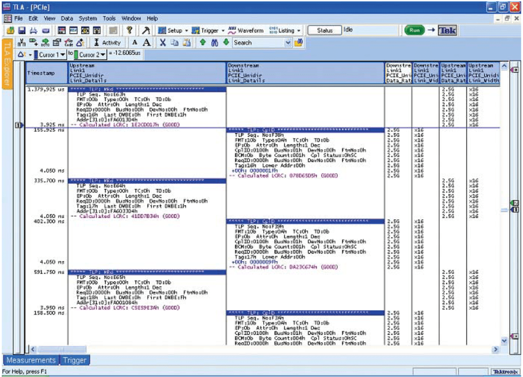
For example, the TLA Series serial analyzer modules provide an innovative approach to PCI Express validation that spans all layers of the protocol from the physical layer to the transaction layer.
Additionally, the TLA Series serial analyzer modules have unsurpassed ability to capture and trigger on PHY layer events, whether problems exists during link training or while the link is going into or out of power management states. Complete support for L0s and L1 power management is “critical as power saving techniques become more prevalent in system designs. The TLA7Sxx Series serial analyzer “acquisition capability is complemented by analysis tools which provide protocol decode and error reporting capabilities, as shown in Figure 35.
Mastering Digital Complexity with the Right Logic Analyzer
Logic analyzers are an indispensable tool for digital troubleshooting at all levels. As digital devices become faster and more complex, logic analyzer solutions must respond. They must deliver the speed to capture the fastest and most fleeting anomalies in a design, the capacity to view all channels with high resolution, and the memory depth to untangle the relationships between tens, hundreds or even thousands of signals over many cycles.
This document has referenced the Tektronix TLA Series of logic analyzers which meet these requirements. We have seen how variables such as triggering (and the way it is used), high-resolution sampling, and innovations such as simultaneous timing and state acquisition through one probe can contribute to the logic analyzer’s effectiveness.
Triggering can confirm a suspected problem or discover an entirely unexpected error. Most importantly, triggering provides a diverse set of tools to test hypotheses about failures, or locate intermittent events. A logic analyzer’s range of triggering options is a hallmark of its versatility.
High-resolution sampling architectures such as MagniVu acquisition can reveal unseen details about signal behaviors. Sampling more frequently, as MagniVu acquisition does, offers more opportunities to detect changes—intentional or otherwise—in binary data.
Single-probe acquisition of both state and high-speed timing data is a concept whose time has come. Increasingly this capability is helping designers gather volumes of data about their devices, then analyze the relationship between the timing diagram and the higher-level state activity. Other correlated views also support troubleshooting: time-correlated analog and digital waveforms, listing and protocol views, multi-channel eye diagrams, real-time software traces, histograms, and more.
A host of other characteristics such as acquisition memory, display and analysis features, integration with analog tools, and even modularity join forces to make logic analyzers the tool of choice to find digital problems fast and meet aggressive design schedules. The industry-leading TLA Series of logic analyzers have risen to meet today’s challenges, and will continue to address new challenges as they emerge.
Ready to debug and verify your complex digital designs? Explore our range of logic analyzers, engineered with the channel count, deep memory, and advanced triggering to solve your toughest challenges.
Unsure which channel count, memory depth, or probing is right for your project? Our application experts are ready to help you configure the perfect solution with confidence.
Copyright © Tektronix. All rights reserved. Tektronix products are covered by U.S. and foreign patents, issued and pending. Information in this publication supersedes that in all previously published material. Specification and price change privileges reserved. TEKTRONIX and TEK are registered trademarks of Tektronix, Inc. All other trade names referenced are the service marks, trademarks or registered trademarks of their respective companies.
10/10 52W-14266-5