Introduction
Measuring DC and capacitance parameters for high power semiconductor devices requires sufficient expertise to optimize the accuracy of various measurements. Even for those with this level of expertise, managing set-up changes between ON-state, OFF-state and capacitance-voltage (C-V) measurements can be time consuming and prone to errors; this is especially true in the on-wafer environment.
This application note provides an overview of how the Keithley 8020 High Power Interface Panel greatly simplifies the user test experience by:
- Integrating key measurement-enabling accessories for ON-state, OFF-state and C-V measurements
- Enabling all C-V measurement parameters, at both the component-level and circuit-level, with minimal connection changes at the device under test (DUT)
- Building in flexibility with a variety of connector options
- Expanding easily to support future measurement requirements and new device terminals
Configuring Common Semiconductor Device Measurements using Traditional Accessories and Standalone Instrumentation
A review of the requirements for the DC and capacitance measurements to be made on the DUT is an important first step.
ON-State Measurements
Characteristic curves for a power transistor, FET, or diode include a plot of its typical output characteristics. Output characteristics for some power devices can involve tens to hundreds of amps. Therefore, creating these curves requires a high current instrument, such as the Keithley 2651A High Power System SourceMeter® instrument; when two 2651As are configured in parallel, they can generate up to 100 A in pulsed current. This SMU instrument is coupled with a lower power SMU instrument, such as Keithley's 2636B, to drive the control terminal (e.g., gate) of a three-terminal device.
To produce optimal high current measurements, managing the resistance and inductance in the cabling is imperative. This can be achieved using low inductance coaxial Kelvin connections and minimizing the inductive loop area at the DUTs. (Probe station geometries often dictate this inductive loop area.) The gate SMU instrument also requires Kelvin connections so that high current pulses at the FET's source terminal don't affect the gate voltage and change the operating point of the device.
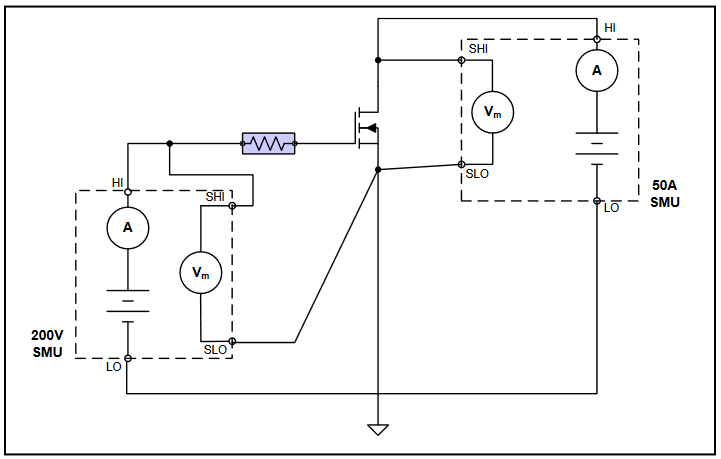
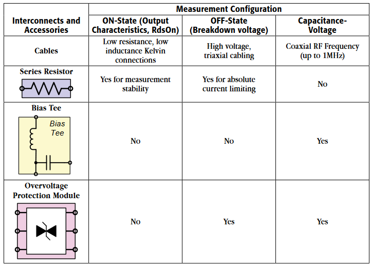
High power devices often exhibit high gain and may be prone to oscillation during testing. Adding series resistors helps eliminate such oscillation. In typical test systems, the resistor is inserted between the lower power SMU instrument and the gate terminal. This resistor must be housed in a shielded enclosure so that electrostatic interference is not coupled in when characterizing other parameters, such as gate leakage. Otherwise, the series resistor would have to be removed for those other tests. Series resistance values can vary between devices and it may be necessary to try several values in order to select the appropriate value. It can be a design challenge to house and connect to these resistors properly when performing on-wafer measurements. Figure 1 illustrates the typical setup for high current ON-state measurements.
OFF-State Measurements
OFF-state characterization includes measurement of the breakdown voltage and leakage current of the device. These parameters are typically tested at the device's maximum rated voltage, which can be hundreds to thousands of volts. A high voltage SMU instrument, such as Keithley's 2657A High Power System SourceMeter instrument, which has 3 kV capability, is ideal for measuring the OFF-state parameters. The 2636B SMU instrument can also be used to bias the device in a certain state or to measure current at other device terminals. Because device breakdown can subject this lower power SMU instrument to high voltage from the 2657A, the addition of a protection module is critical to protecting the 2636B from damage.
The breakdown profile of some devices is very sharp, with device impedance changing by several decades in microseconds. Such transitions can exceed the speed of the SMU instrument in transitioning to current limit control, as well as lead to high currents in the test system due to rapid discharge of cable and system capacitance. Inserting a resistor in series with the 2657A enforces an absolute current limit that can protect devices and probes from high transient current. It's important to ensure the resistor is rated for high voltage and is in a grounded enclosure to protect the operator from exposure to high voltage. This will require creating a custom enclosure to mate with the high voltage SMU instrument and the connector at the probe station, as well as extra cables to connect the resistor box to both the instrument and the positioner.
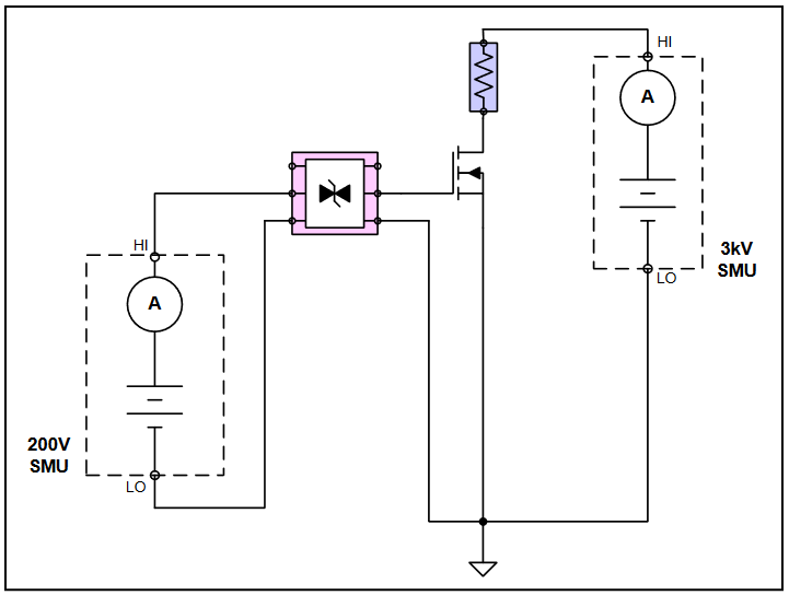
Measurements of leakage current range from picoamps to microamps for most power semiconductor devices. At these levels, system leakage can affect the accuracy of the measurement, requiring the use of low noise triaxial cabling and connections. Both the 2657A and the 2636B have triaxial connectors. Triaxial cabling allows for a driven guard, which shunts extraneous system leakage current from the measurement node and reduces settling time by nulling the effect of cable capacitance. Figure 2 illustrates the typical setup for a high voltage breakdown voltage measurement.
Capacitance-Voltage Measurements
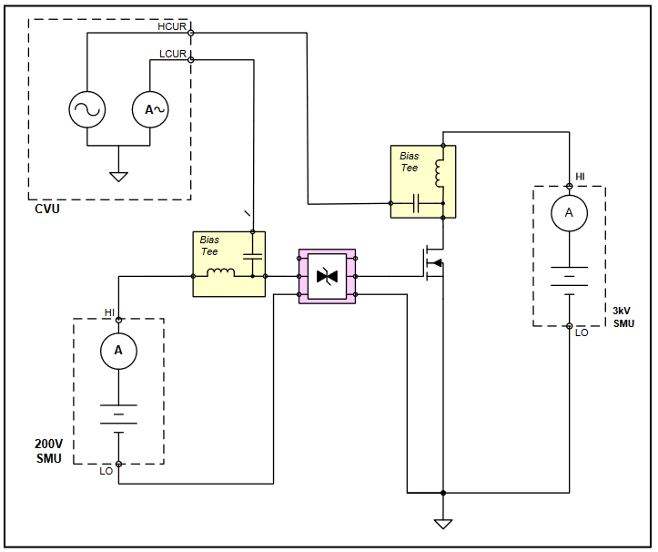
A power MOSFET device engineer or circuit designer may have an interest in various capacitance parameters, including input capacitance (CISS), output capacitance (COSS), reverse transfer capacitance (CRSS), gate-source capacitance (CGS) and drain-source capacitance (CDS). Similar capacitance parameters exist for BJTs and IGBTs. Capacitance changes as a function of voltage and tests are performed up to the rated voltage of the device. The rated voltage of power devices likely exceeds the built-in DC voltage capability of most capacitance meters, so bias tees are required to achieve these measurements. Because of the high voltage involved, it's essential to protect any lower power SMU instruments used in the setup, requiring the use of protection modules to accomplish this task. Figure 3 illustrates a typical high voltage capacitance measurement.
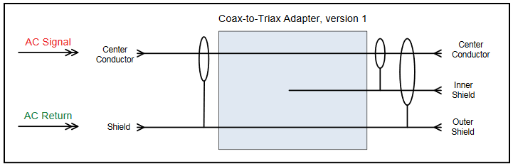
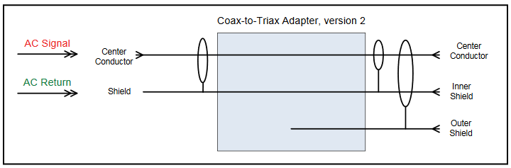
Coaxial cabling and connections are common with capacitance measurements. To minimize series inductance in the measurement, the shields of the coaxial cables are tied together as close as possible to the DUT. If the test fixture or probe station uses triaxial connections, it is important to consider how to adapt coaxial C-V connections to triax. Figure 4 provides the schematic for two available coax-to-triax adapters. In both cases, the adapters must be removed when transitioning to low-level DC current measurements in order to achieve optimal performance. In Figure 4a, the adapter prevents carrying the DC guard to the DUT. Therefore, any measurements made would include error due to system leakage. In Figure 4b, the adapter would result in problems when DC guard is routed to the DUT if the shields were still shorted together at the DUT as necessary for C-V measurements. Therefore, it would be necessary to change connections when moving from C-V to DC to avoid error or SMU instrument damage when moving from C-V to DC I-V measurements.
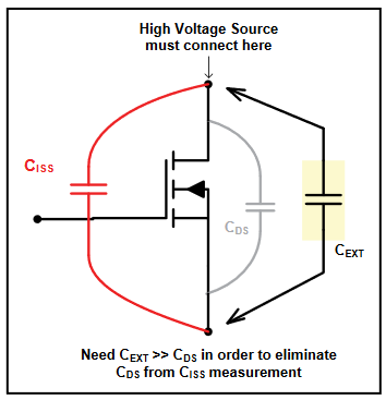
The different capacitance parameters of the device require different connections for AC source and AC measurement terminals of the capacitance meter. These connections must be moved around the device while maintaining bias at the device’s drain or collector. Although capacitance measurements are inherently two-terminal measurements, for three-terminal devices, it’s important to consider the capacitance between either of the two terminals to the third terminal. If this third terminal is not handled from an AC perspective, capacitance to this terminal will be included as an error in the measurement. For example, a CISS measurement on a power MOSFET requires the bias tee at the drain to enable high voltage bias. However, CISS is a combination of the gate-to-source and gate-to-drain capacitance. Therefore, it’s necessary to eliminate the drain-source capacitance (CDS) from the measurement. To eliminate CDS, it’s essential to short this capacitance from an AC perspective while still allowing for hundreds to thousands of DC volts across the same terminals. This requires a high voltage rated capacitor that is of higher capacitance (or lower impedance) than CDS. Note Figure 5for an illustration of the measurement problem. The presence of high voltages also requires that this capacitor be housed in a safe enclosure. Finally, it's necessary to switch out the capacitor when measuring other capacitance parameters on this device. Setting up this measurement is no easy task.
Moving from Measurement to Measurement
A review of Figures 1–3 illustrates the setup changes required when transitioning from ON-state to OFF-state to capacitance measurements. Table 1summarizes the various accessories required throughout the testing of a particular device. It is easy to see how the opportunities for user error can increase with the number of devices to be tested.
Configuring Common Semiconductor Measurements using the 8020 High Power Interface Panel
The 8020 High Power Interface Panel integrates several of the measurement-enabling accessories shown in Table 1, thereby eliminating cable and setup transitions.
The 8020 supports one high voltage SMU instrument (up to 3 kV), up to three lower power 200 V SMU instruments and up to two high current SMU instruments to achieve 100 A pulsed capability. That allows the 8020 to be used in testing a large variety of power devices, especially at the current and voltage levels being tested on wafers.
All channels support full Kelvin (remote sense) connections, so that ON-state measurements can even be performed with 200V SMU instruments (up to 10 A pulse capability).
The 8020 includes built-in over voltage protection for the lower power 200 V SMU channels, eliminating the need for external protection modules and the complications involved in connecting them. Screw terminals located under the interface panel's top cover provide for inserting any two-terminal resistor in series with the high voltage or 200 V SMU channels. Resistors are housed within a safe, shielded enclosure, which manages the safety and electrostatic interference issues associated with using series resistors for oscillation suppression and gate leakage measurements, as well as when using resistors to enforce absolute current limits for breakdown voltage measurements. A high voltage rated resistor kit is provided with the 8020, which includes a wide range of commonly used values so that users can get up and running quickly.
Transient current limit protection is also available on the high voltage and 200 V channels. This can be useful in breakdown voltage testing to protect sensitive probes from the high transient currents that may appear when the device has a sharp breakdown characteristic. This transient protection affects currents greater than 100 mA with transitions less than 100 μs. This protection can also be easily bypassed in order to achieve the maximum pulse current rating on the 200 V channels.
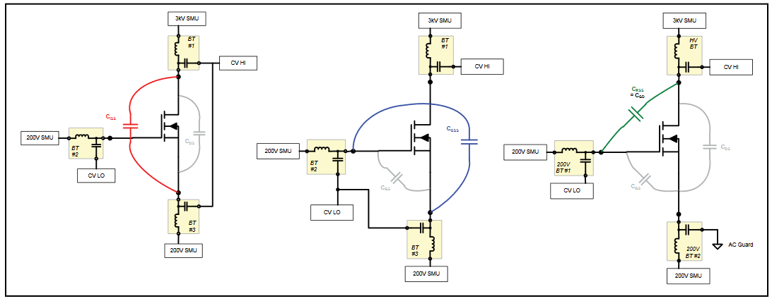
One of the key advantages the 8020 offers is evident when measuring capacitance. Rather than employing a single bias tee at the high voltage terminal of the device, the 8020 includes a bias tee at each of the high voltage and 200 V channels to allow a bias tee at up to four device terminals. Having a bias tee at each device terminal improves isolation between the capacitance meter and the SMU instrument. When transitioning between measurements of different capacitance parameters, the connections between the 8020 and the DUT remain static. The setup transition between the tests of several capacitance parameters occurs at the input of the bias tee, where the user can easily manipulate the AC source and measurement terminals of the capacitance meter using connectors that are low voltage and fixed. Figure 6 depicts connection changes between circuit level capacitance parameters (CISS, COSS, CRSS). Note that connections at the device do not change.
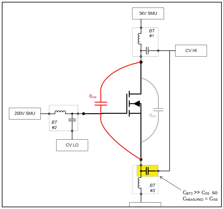
Allowing a bias tee at each device terminal also simplifies the capacitance measurement. As shown in Figure 5, a CISS measurement requires a fairly large high voltage rated capacitor to short out CDS from an AC perspective. Using bias tees at every terminal allows for the use of the bias tee capacitance as an AC short. This is accomplished by using a single coaxial cable to connect the AC inputs of the bias tees, which are connected to the drain and source terminals. See Figure 7.
Capacitance measurements are available on triaxial connectors with the 8020. The return of the capacitance meter is routed on the outside shield of the triax, and this eliminates the need for coax-to-triax adapters, as well as cabling changes between DC I-V measurements and C-V measurements. This means that the shields can remain shorted together for C-V measurement without negatively impacting DC I-V measurements.
Typical bias tees induce significant leakage current. The bias tees used in the 8020 are of guarded triaxial design and have programmable multi-mode capability so that low current DC OFF-state measurements, ON-state DC measurements, and high voltage C-V measurements can be made through the bias tee without changing the connections between the 8020 and the DUT (except for connection of the 2651A to the FET's drain terminal when performing ON-state measurements).
In addition to these testing advantages, the 8020 manages common LO reference for all the SMU instruments that connect to it. It manages the system interlock so that a single normally-open switch at the device access point can disable the high voltage output of all connected SMU instruments. The 8020 also has daisy chain capabilities, which allows for system expansion when it's necessary to add SMU channels to the system. It continues to manage the common LO reference and system interlock across all connected 8020 mainframes.
The 8020 provides the flexibility to mate with a variety of connectors. The lack of standardized commercial connectors for high voltage and high current measurements means probe station positioners and test fixtures have a variety of connector options. Because the 8020 has several connector card options for use with high voltage, 200 V, and common LO channels, it can be used with a variety of probe stations or with a custom fixture.
Conclusion
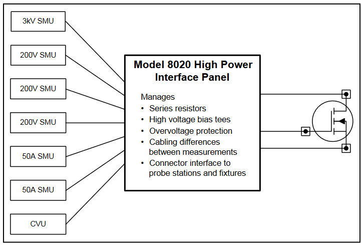
The 8020 High Power Interface Panel greatly reduces the frustration test engineers encounter when performing comprehensive DC I-V and C-V testing of power semiconductor devices. The role of the 8020 for on-wafer power device measurements is shown in Figure 8. By integrating the capabilities of several measurement-enabling accessories, the 8020 minimizes both connection changes and opportunities for user error in technology development applications.