
お問い合わせ
ダウンロード
マニュアル、データシート、ソフトウェアなどのダウンロード:
フィードバック
PSPL5868 10.7 Gb/s Driver Amplifier Datasheet
PSPL5868 Datasheet
このデータ・シートの製品は、テクトロニクスでは販売終了となっています。
Tektronix Encoreプレミアム再生品を見るbr/>
上記製品のサポートと保証のステータスをチェックする
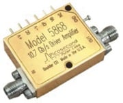
The Model PSPL5868 driver amplifier is intended for use as a modulator driver or as a linear amplifier. This device includes internal temperature compensation for excellent output stability over temperature, and exhibits both high output and low power dissipation. It also incorporates internal sequencing circuitry, making it insensitive to power supply application sequence.
Key performance specifications
- 11 V output amplitude 10.7 Gb/s Modulator Driver
- Linear amplifier with 28 dB gain
- 30 kHz to 11.8 GHz bandwidth
- Temperature compensated design for output stability
- Includes bias network, crossing point control & adjustable output voltage
Typical 10.7 Gb/s eye measurements
Input from Tektronix PPG1601, PRBS = 223–1, 750 mV

Output amplitude, 11 V
Typical performance

Typical small signal S21 (measured at –20 dBm input power)

Typical small signal S11 and 22 (measured at –20 dBm input power)
Typical performance plots

Output voltage vs. Input voltage (Gain control bias = Vgc, TCASE = 35 °C

Crossing point vs. Vcp
Instructions
The PSPL5868 10.7 Gb/s modulator driver can be operated using only three of the available 7 pins. The DC pins required for operation are 1, 3, and 7. The RF connectors and DC pins are shown in the following drawing and table. Warning: To prevent damage, provide a ground connection at pin 7 before applying voltage to the PSPL5868.

| Pin # | Pin Lable | Description |
|---|---|---|
| IN | SMA, signal input, Vamp≤ 1.5 V (damage threshold) | |
| 1 | +V | Positive DC voltage supply, 8.25 V 12 |
| 2 | GC | VgcVariable output control, -15 V ≤ Vgc ≤ 0 V 3 |
| 3 | -V | Negative DC voltage supply, -5.25 V ≤ V ≤ -4.75 V 2 |
| 4 | CP | Crossing point adjust, -5 V ≤ Vcp ≤ 5 V 4 |
| 5 | VB | DC Voltage bias, -17 ≤ VB ≤ +33 5 |
| 6 | NC | No connection / Not used |
| 7 | GND | Ground connection |
| OUT | SMA, signal output |
1 At 8.25 V, approximately 3 W is dissipated.
2 No power sequencing is necessary. Voltages may be applied in any order after ground is applied.
3 Output Control: With VGC at 0 V, or left floating (disconnected), the driver will provide maximum gain and maximum output voltage. The user can decrease VGC to decrease the RF signal gain when the driver is operating in the linear regime, or to reduce the output voltage level when the driver is operated in saturation (this will also reduce the power dissipated).
4 The crossing point may vary until unit achieves thermal equilibrium. VCP > 0 V will lower the output crossing point and increase power dissipation. Care must be taken to ensure that the positive supply current does not exceed 400 mA.
5 Voltage Bias: The VB pin allows the user to apply a low current (less than 3.5 mA) DC offset to the Signal Output for biasing electro-optic modulators through a 2.5 kΩ resistor.
Specifications
| Parameter | Symbol | Units | Minimum | Typical | Maximum | Comments |
|---|---|---|---|---|---|---|
| Impedance | Z | ohms | 50 | |||
| Upper 3 dB freq. | fc,h | GHz | 11.8 | Relative to gain at 2 GHz | ||
| Lower 3 dB freq. | fc,l | kHz | 30 | Relative to gain at 2 GHz | ||
| Small signal gain | S21 | dB | 28.5 | Measured at 2 GHz | ||
| Max Power Out (-1 dB gain comp) | P1 dB | dBm | 24.4 | Measured at 2 GHz | ||
| Output Eye Voltage with VGC = 0 V | VOUT | Vamp | 10.5 | 11 | Vin = 0.75 Vamp, 10.7 Gb/s PRBS | |
| Output Eye Voltage with VGC = -15 V | VOUT | Vamp | 1.5 | 2.5 | Vin = 0.75 Vamp, 10.7 Gb/s PRBS | |
| Return Loss, Input and Output | S11, S22 | dB | -16 -11 |
50 MHz 5 GHz ≤ f | ||
| Rise Time | tr | ps | 31 | 10-90%, Vin = 0.75 Vamp, 10.7 Gb/s PRBS | ||
| Fall Time | tf | ps | 36 | |||
| Additive Jitter RMS Peak-to-Peak |
ps pspp |
1.5 8 |
Vin = 0.75 Vamp, 10.7 Gb/s PRBS, measured at crossing point | |||
| Overshoot | % | 5 | 10.7 Gb/s PRBS | |||
| Undershoot | % | 5 | 10.7 Gb/s PRBS | |||
| Eff. Input RMS Noise Voltage | μV rms | 152 | ||||
| Noise Figure | NF | dB | 5.75 | f = 1 GHz | ||
| Output Eye Voltage Variation | Δ VOUT | % | ±5 | Vgc = 0 V, Vin = 0.75 Vamp, TCASE = -5 to 75 °C | ||
| Crossing Point Adjust | % | ±12 | -13.5 / +17.5 | ±5 V input at Vcp, Vin = 0.5 Vamp | ||
| Crossing Point Variation | % | ±5 | Vin = 0.75 Vamp, 10.7 Gb/s PRBS, TCASE = -5 to 75 °C | |||
| Polarity | Non-Inverting | |||||
| Coupling | AC, input and output | |||||
| RF Connectors | SMA jacks (f) | |||||
| DC Connector | Solder pins | |||||
| Voltage Supply (+) | +VDC | V | 8 | 8.25 | 8.5 | |
| Voltage Supply (-) | -VDC | V | -5.25 | -5 | -4.75 | |
| Supply Current (+) | +IDC | mA | 325 | Vout = 11 Vamp 1 | ||
| Supply Current (-) | -IDC | mA | 20 | |||
| Power Dissipation | Pdiss | W | 3 | 3.3 | Vout = 11 Vamp 2 | |
| Max Allowed Input | Vamp | 1.5 | Input damage threshold | |||
| Output Voltage Bias | Vbias | VDC | -17 | 0 | 33 | No connection required 3 |
| Gain Control Bias | Vgc | VDC | -15 | 0 | 0 | No connection required |
| Crossing Point Bias | Vcp | VDC | -5 | 0 | 5 | No connection required |
| Operating Temp | TCASE | °C | -5 | 75 | Case temperature | |
| Storage Temp | Tstor | °C | -40 | 125 | ||
| Warranty | One year | |||||
1 The PSPL5868 can be damaged by excessive heat that is produced when driving low duty cycle positive pulses. To ensure the amplifier will not be damaged by overheating, it is recommended the positive supply voltage has its current limit set to 400 mA.
2 Vgc can be used to lower the output level and power dissipated. Vcp > 0 V will lower the crossing point and increase the power dissipated.
3 A 2.5 kΩ resistor is connected to the output from the Vbias pin for adding a low current (≤ 3.5 mA) DC bias.
Mechanical dimensions

Ordering information
Models
- PSPL5868
- DRIVER AMPLIFIER, 10.7 Gb/s