Contactez-nous
Chat en direct avec un représentant Tek. Service disponible de 9 h à 17 h, CET jours ouvrables.
Appelez-nous au
Disponible de 9 h à 17 h CET jours ouvrables.
Télécharger
Télécharger des manuels, des fiches techniques, des logiciels, etc. :
Feedback

Des mesures PCI Express précises et répétables
Depuis près de vingt ans, la technologie PCI Express® est devenue la norme de facto des connexions série haute vitesse. Les dernières spécifications PCIe® portent sur l'usage intensif des données, notamment pour l'intelligence artificielle/le machine learning et le calcul intensif.
Nos solutions de test automatisées PCIe réduisent considérablement la complexité des tests en gérant la configuration et l'étalonnage. Associées à un matériel de mesure à faible bruit, ces solutions permettent des mesures d'intégrité du signal rapides, précises et répétables. En tant que membre actif et votant des groupes de travail PCI-SIG®, nous disposons de l'expertise indispensable pour la validation des transmetteurs, des récepteurs, des horloges de référence et de boucle de verrouillage de phase (PLL).
PCI Express, PCIE et PCI-SIG sont des marques déposées et/ou de service de PCI-SIG.
Solutions complètes de tests automatisés pour PCIe
Solutions de test de transmetteurs et de récepteurs PCIe 6.0 Base et CEM de pointe
PCIe® 6.0 est une norme d'interface série polyvalente et à grande vitesse utilisée pour connecter divers composants au sein des systèmes informatiques modernes, qui utilise la signalisation PAM4 et la correction d'erreur directe (FEC) pour atteindre un taux de transfert de données révolutionnaire de 64,0 GT/s, ce qui permet un traitement plus rapide et des performances plus fluides pour les applications exigeantes.
Les outils intuitifs de Tektronix permettent de prendre immédiatement des mesures telles que le rapport de distorsion signal/bruit (SNDR), la gigue non corrélée, l'étalonnage TP3/TP2 de signal contraint à diagramme en œil du récepteur et la compensation du bruit d'instrumentation exigée par les dernières spécifications.
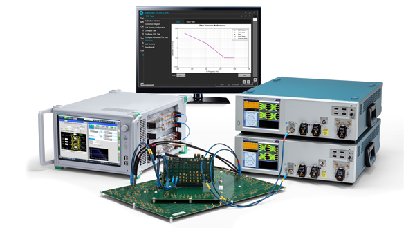
Comme pour les générations précédentes, les tests de conformité et de validation PCIe 6.0 sont essentiels pour garantir le respect des normes définies par le PCI-SIG, tant pour BASE que pour CEM. La solution de test de transmetteur (Tx) PCIe 6.0 de Tektronix permet aux ingénieurs de résoudre les derniers problèmes de conception et de validation. Pour la solution de test du récepteur PCIe 6.0, Tektronix et Anritsu ont collaboré pour proposer une solution de test Rx supérieure en associant l'oscilloscope en temps réel DPO70000SX de Tektronix avec le testeur de taux d'erreur binaire MP1900A d'Anritsu, tous deux contrôlés par des outils d'automatisation et d'analyse des tests développés et pris en charge par Tektronix.
Solution de récepteur (Rx) PCIe 6.0
Solution de transmetteur (Tx) PCIe 6.0
Contactez-nous au sujet de votre application de test PCIe 6.0.
Solutions de test de transmetteur PCIe
Nos solutions de test de transmetteur PCIe assurent la compatibilité en amont avec la validation de transmetteur PCIe et les solutions de conformité, de 2,5 à 64,0 GT/s (première à sixième générations). Prend en charge des plages, de la caractérisation initiale de la tension et de la synchronisation du silicium aux mesures du transmetteur au niveau plateforme et de l'horloge de référence. Les responsables technologiques de Tektronix tiennent à jour ces solutions en incorporant tous les avis de modification technique (ECN) et les recommandations des ateliers de conformité PCI-SIG pour l'approbation des solutions.
Le nouvel oscilloscope DPO Série 7 offre des solutions de validation et de conformité des transmetteurs PCIe Gen 1 à 4 pour prendre en charge les mesures BASE, CEM et d'horloge de référence.
Fiche technique PCIe Gen 1 à 6
Brochure de test de conformité PCIe Gen 5 Tx
Oscilloscopes hautes performances DPO70000SX ATI
Oscilloscopes au phosphore numérique et à signaux mixtes MSO/DPO70000DX
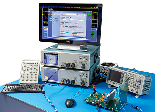
Solutions de test de récepteur PCIe et PLL
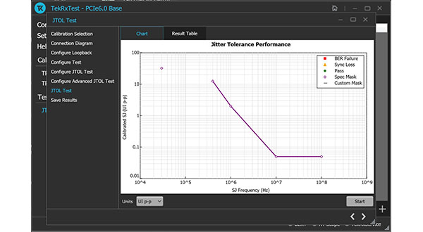
La validation de récepteur PCI Express est notoirement difficile en raison de la sensibilité nécessaire à l'étalonnage d'un signal contraint à diagramme en œil sur une voie à forte perte. Les solutions Tektronix de test de récepteur PCI-e permettent d'avoir l'assurance que votre conception a été testée de façon exhaustive conformément à la cible d'erreurs binaires (BER). Nos outils intuitifs avec instructions détaillées incluent des routines d'apprentissage de liaison pour le testeur de taux d'erreur binaire (BERT) Anritsu MP1900A, afin d'assurer un test précis de votre récepteur. Les tests automatisés prennent en charge l'étalonnage des signaux contraints à diagramme en œil, les tout nouveaux tests de conformité d'égalisation de la liaison du transmetteur et du récepteur, des variantes de cibles d'erreurs binaires et la caractérisation de la tolérance de gigue. Ce cadre permet également de mesurer simplement la bande passante PLL et ses pics.
Voir le webinaire sur le récepteur PCIe de 5e génération
Afficher la fiche technique du récepteur PCIe de 1re à 6e génération
Oscilloscopes hautes performances DPO70000SX ATI
Oscilloscopes au phosphore numérique et à signaux mixtes MSO/DPO70000DX
CXL (Compute Express Link)
Les architectures de centres de données doivent faire face à l'accroissement des mouvements de données et demandes d'accès tout en réduisant la consommation, augmentant l'efficacité et prenant en charge des applications plus volumineuses et diverses. En s'appuyant sur la puissance de la couche physique PCI Express, CXL gère ces contraintes en permettant aux processeurs d'accéder à la même ressource de mémoire efficacement, de communiquer et de s'exécuter sur une seule architecture. Les solutions pour couche physique de Tektronix prennent en charge CXL, le débit binaire le plus élevé à 32 GT/s, et les formats divers attendus pour cette nouvelle technologie.
Oscilloscopes hautes performances DPO70000SX ATI
Oscilloscopes au phosphore numérique et à signaux mixtes MSO/DPO70000DX