The ability to present both analog and digital representations of signals make mixed signal oscilloscopes (MSOs) ideal for verifying and debugging digital circuits.
This application note provides tips to help you efficiently debug your digital designs using MSOs. It covers important setup considerations such as logic threshold settings, clocking, and channel deskew. It explains how to trigger on minimum pulsewidth violations, setup and hold violations, and verify output codes on an analog to digital converter through a series of examples.
The Tektronix 5 Series MSO and MSO2000 and MSO5000 Series of mixed signal oscilloscopes combine the performance of a Tektronix oscilloscope with the basic functions of a 16-channel logic analyzer. The Tektronix MDO3000 and MDO4000 Series also offer 16-channel logic analyzer capabilities. Throughout this application note, any features or capabilities referred to in MSOs are also available in MDO products.


Setting Digital Thresholds
A mixed signal oscilloscope's digital channels view a digital signal as either a logic high or logic low, just like a digital circuit views the signal. This means as long as ringing, overshoot and ground bounce do not cause logic transitions, these analog characteristics are not of concern to the MSO. Just like a logic analyzer, an MSO uses a threshold voltage to determine if the signal is logic high or logic low.
The 5 Series MSO and MSO5000 and MDO4000 Series provide per-channel threshold settings that are useful in debugging circuits with mixed logic families. Figure 1 shows the MDO4000 measuring five logic signals on one of its digital probe pods. Three TTL (Transistor-Transistor Logic) signals and two LVPECL (LowVoltage Positive Emitter-Coupled Logic) signals are measured at the same time.
For the MSO2000 and MDO3000 Series, the thresholds are adjusted per probe pod (a grouping of 8 channels) and therefore, the TTL signals would be on one pod while the LVPECL signals would be on the second pod.
Timing and State Acquisitions
Logic analyzers provide two different digital acquisition techniques. The first technique is timing acquisition in which the analyzer samples the digital signal at uniformly spaced times determined by the instrument's sample rate. At each sample point, the logic analyzer stores the signal's logic value and it uses these samples to create a timing diagram of the signal.
The second digital acquisition technique is state acquisition. State acquisition defines special times that the digital signal's logic state is valid and stable. This is common in synchronous and clocked digital circuits. A clock signal defines the time when the signal state is valid. For example, the input signal stable time is around the rising clock edge for a D-Flip-Flop with rising edge clocking. The output signal stable time is around the falling clock edge for a D-Flip-Flop with rising edge clocking. Since the clock period of a synchronous circuit may not be fixed, the time between state acquisitions may not be uniform as it is in a timing acquisition.
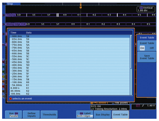
A mixed signal oscilloscope's digital channels acquire signals similar to how a logic analyzer acquires signals in timing acquisition mode, as seen in Figure 2. For applications in which state information is needed, Tektronix MDO/MSO Series oscilloscopes can decode the timing acquisition into a clocked bus display (Figure 2) and event table (Figure 3) which is similar to the logic analyzer's state acquisition display.
Color-Coded Digital Waveform Display
Digital timing waveforms look very similar to analog waveforms except only logic highs and lows are shown. Timing acquisition analysis often focuses on determining logic values at specific points in time and measuring the time between edge transitions on one or more waveforms. To make analysis easier, the Tektronix MDO/MSO Series shows logic lows as blue and logic highs as green on the digital waveforms, allowing you to see the logic value even if a transition is not visible. The waveform label color also matches the probe color-coding to make it easier to see which signal corresponds to which test point, as shown in Figure 4.
The digital timing waveforms can be grouped to create a bus. One digital signal is defined as the least significant bit and the other digital signals represent the other bits of the binary number up to the most significant bit. The oscilloscope will then decode the bus into a binary or hex value. The Tektronix MDO/MSO Series also creates an event table, displaying the logic states as a binary or hex value. Each state is time-stamped, simplifying timing measurements.
The Tektronix MSO Series decodes parallel buses using clocked or unclocked formats. For clocked decoding, the oscilloscope determines the logic state of the bus at either the rising edge, falling edge or both edges of the signal you specify as the clock.

This means only the valid transitions on the bus are shown, excluding any transitions that happen when the data is not valid. For unclocked decoding, the oscilloscope decodes the bus at every sample point, showing every transition on the bus. When the oscilloscope uses clocked decoding, the decoded bus display and event table are very similar to the state display of a logic analyzer. Since bus decoding is a post-acquisition process, you have the flexibility to change the decoding format during analysis.
The Tektronix MDO/MSO Series simultaneously decodes up to two to sixteen buses, depending on the model. The buses are defined as parallel or serial (I2 C, SPI, USB, CAN, LIN, FlexRay, RS-232/422/485/UART, Ethernet, MIL-STD-1553, and I2 S/LJ/RJ/ TDM). A parallel bus is composed of any of the digital channels D0 through D15. A serial bus is composed of any of the analog channels 1 through 4 and the digital channels D0 through D15. The MSO2000, MDO3000, and MDO4000 Series provide maximum design visibility by displaying up to four analog channels, four reference waveforms, one Math waveform, three buses and 16 digital channels at one time. The MSO5000 Series provides even greater analysis capabilities, with up to four Math waveforms and 16 buses at once. The 5 Series MSO provides up to 8 analog channels, up to 64 digital, and many math and decoded bus waveforms at once.
Preparing for Digital Acquisition
There are two basic tasks to prepare an MDO/MSO for digital acquisition. First, just like a logic analyzer, the MSO digital channel thresholds are configured for the logic family being measured to ensure the correct logic level is acquired. Second, the analog channel's skews are adjusted for accurate time correlation between the analog channels and the digital channels.
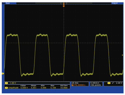
The MDO/MSO's analog channel is used to quickly check the logic swing of your digital signal. In Figure 5, the oscilloscope automatically measures the 5 V CMOS signal amplitude with measurement statistics across multiple acquisitions. For logic families with symmetrical voltage swings like CMOS, the threshold is at half of the signal amplitude. In Figure 6, the digital channel threshold is set to 2.5 V which is half the amplitude of the 5 V CMOS signal. However, for logic families with asymmetrical voltage swings like TTL, you typically need to consult the component data sheet and define the threshold as half-way (TTL Vthreshold = 1.4V) between the logic device's maximum low-level input voltage (TTL VIL = 0.8V) and minimum high-level input voltage (TTL VIH = 2.0V) values.
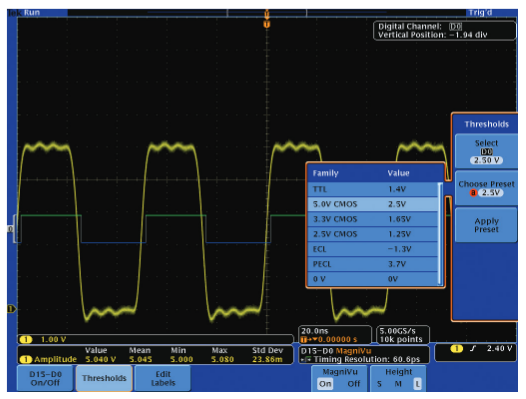
In Figure 6, you can see the timing skew between the rising edges of the analog and digital waveforms of the same signal. The analog waveform is leading the digital waveform. For accurate measurements, it's important to remove the analog to digital time skew for better time-correlation measurements between the analog and digital waveforms. The Tektronix MDO/MSO Series provides adjustable analog probe deskew to align the analog channels with each other and to align the analog channels with the digital channels. The analog channel deskew settings compensate for different analog probe propagation delays.
Every Tektronix MDO/MSO Series oscilloscope has a compatible logic probe. To simplify digital measurements, the oscilloscope compensates for the propagation delay of the logic probe. Therefore, there are no digital channel probe deskew adjustments.
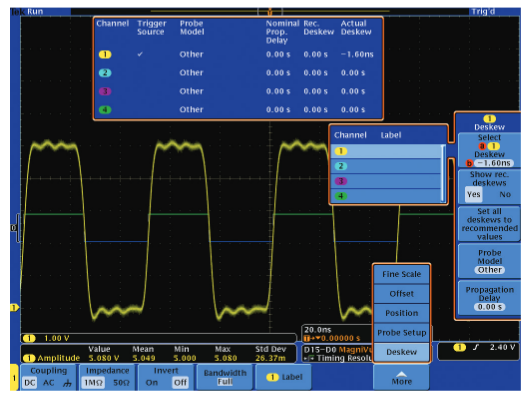
To align the analog channels with the digital channels, the 2.5 V 50% amplitude position on the CMOS analog waveforms are time aligned with the CMOS logic transitions which occur at the 2.5 V threshold. As shown in Figure 7, a -1.60 ns deskew is used to align the analog channel to the digital channel. This deskew process is repeated for the other analog channels.
The analog channel's skews should be checked when the analog probes are changed and the digital thresholds should be checked when measuring a different logic family. With the threshold and skews configured, the oscilloscope is ready for verifying and debugging digital circuits.
Measurement Examples
Triggering on Pulse Width Violations
The first example is verifying a TTL burst signal that contains eight positive pulses as shown in Figure 8. The positive pulse width specification range is 23.2 ns to 25 ns with 26 ns to 27 ns between the pulses. The time between the bursts is not specified.

The MSO digital channel is connected to the TTL burst signal and the threshold is set for TTL logic. The oscilloscope is configured for rising edge trigger. To speed up the verification process, the oscilloscope is configured to automatically measure the positive and the negative pulse widths between the cursors.
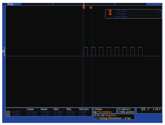
Figure 9 shows a single shot acquisition where the oscilloscope triggered on the first pulse edge. Depending upon when the single shot acquisition button was pushed, the oscilloscope could have triggered on any of the other rising edges.
The acquired signal has eight pulses which comply with the specification. The first positive pulse width is 23.88 ns and the negative pulse width is 26.18 ns which are automatically measured. These values are within the specifications. The Tektronix MDO/MSO Series oscilloscope's cursors are linked and one control moves both cursors down the waveform checking each positive and negative pulse width. All pulses in this acquisition meet the specification.
The positive and negative pulse widths are more rigorously checked by changing the MSO acquisition mode from Single to Run. The positive and negative pulse statistics (mean, minimum, maximum and standard deviation) are accumulated across multiple acquisitions. You can select between 2 to 1,000 acquisitions for the measurement statistics.

Figure 10 measurement statistics show the positive pulse width mean is 23.87 ns with a 53.62 ps standard deviation. The positive pulse width minimum is 23.76 ns and the maximum is 24.00 ns which are within the specifications. Likewise, the negative pulse width measurements are verified to be within the specifications. At this point, the verification of the TTL burst signal is progressing smoothly.
This verification technique depends on which parts of the continuous signal are being acquired and analyzed. A more robust verification technique is to have the Tektronix MDO/MSO Series check every pulse with its powerful triggering capabilities. For example, the oscilloscope can be set up to verify the TTL burst signal by measuring each and every positive pulse and triggering on non-conforming pulse widths smaller than 23.2 ns. The single shot acquisition mode is used to stop the MSO after it triggers, allowing the non-conforming pulse to be analyzed.
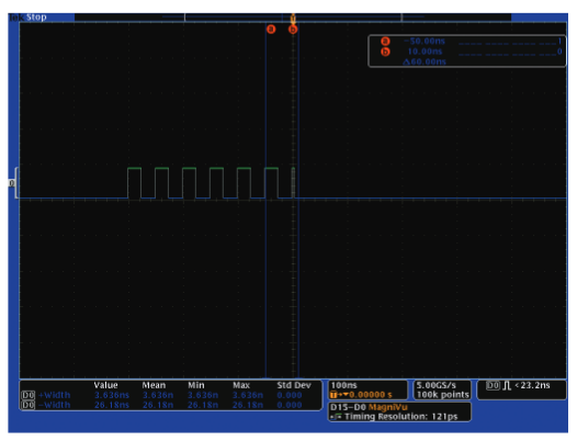
In Figure 11, the oscilloscope triggered on a non-conforming positive pulse less than 23.2 ns. Two errors are captured in this acquisition. The first error is that the seventh pulse is 3.636 ns wide which is smaller than the 23.2 ns minimum specification.
The second error is the missing eighth pulse. This is an example of using the digital triggering to look for non-conforming digital signals. Also, in looking for non-conforming digital signals, the MSO trigger can be used to look for pulses greater than 25.6 ns. In this case, no problems were found.
The root cause of this error is a design flaw. The signal that controlled the gating of the pulses was asynchronous to the generation of the pulses and it occasionally varied in its gating duration. As a result, the internal gating signal intermittently chopped off the last pulse and clipped the seventh pulse.
This verification technique of triggering on errors can be used to monitor the signal for long durations, such as overnight or over the weekend, to provide even more rigorous verification of the design.
Combining Analog and Digital Waveforms to Identify Crosstalk
In this example, two Low-Voltage Positive Emitter-Coupled Logic (LVPECL) signals are verified. The 3.3 V LVPECL logic high is approximately 2.4 V and the logic low is approximately 1.6 V. Therefore, the digital channels thresholds are set to 2.0 V.
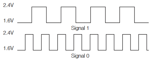
Signal zero is a square wave with approximately 50 ns period and signal one is a square wave with approximately 90 ns period as shown in Figure 12. There is no fixed time relationship between the signals.
The same verification technique that was used in the previous TTL burst example is used to verify these LVPECL signals. To check for non-conforming signals, the oscilloscope is configured to trigger on a pulse width less than 22.4 ns. In Figure 13, the MSO triggered on a 727.3 ps glitch on the bottom signal. Capturing this glitch required the oscilloscope to have a timing resolution that is better than 727.3 ps.
An important acquisition specification is the timing resolution used for capturing digital signals. Acquiring a signal with better timing resolution provides a more accurate timing measurement of when the signal changes. For example, a 500 MS/s acquisition rate has 2 ns timing resolution and the acquired signal edge uncertainty is 2 ns. A smaller timing resolution of 60.6 ps (16.5 GS/s) decreases the signal edge uncertainty to 60.6 ps and captures faster changing signals.
The Tektronix MSO5000 and MDO4000 Series internally acquire digital signals with two types of acquisitions at the same time. The first acquisition is with timing resolution down to 2 ns for a record length up to 250 M. The second acquisition is called MagniVu™ high speed acquisition. The MagniVu timing resolution is down to 60.6 ps with up to a 10,000 point record length acquisition centered on the trigger. The MDO3000 Series provides MagniVu timing resolution up to 121.2 ps. The MagniVu acquisition shows signal transition details like glitches that are not seen by other instruments with less timing resolution.

In Figure 13, the bottom signal glitch occurs at the same time that the rising edge of the top signal occurred. This could be a crosstalk problem but more information is needed before making this diagnosis.
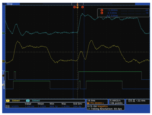
The analog channels are connected to both LVPECL signals and the oscilloscope is started again looking for small non-conforming pulses. This time the oscilloscope triggered on a 1.091 ns glitch and provides analog insight into both LVPECL signals as shown in Figure 14. Analog glitches occur at the same time that the rising edges occur on the other signal. Most of these analog glitches are below the LVPECL logic threshold, but some of these glitches cross the logic threshold and are seen as logic errors such as the glitch on the top waveform at the left edge of the display.
The MDO/MSO provides the significant advantage of capturing both the signal's digital and analog characteristics and displaying them time correlated, providing insight into the signal integrity of the digital signals. The root cause of these glitches are rising edge crosstalk between the two LVPECL signals. The LVPECL rising edge transitions are driven harder and faster than the falling edges. As a result, the rising edges create significantly more crosstalk than the falling edges. There is no indication of falling edge crosstalk in this acquisition.
Capturing Non-Monotonic Edges and Setup/Hold Violations

In this example, the operation of a TTL 74F74 D-Flip-Flop is verified. The D-Flip-Flop rising clock edge loads the D input into the Q output as shown in Figure 15. For example, the Q output is high if the D input is high at the time of the rising clock edge.
Figure 16 shows the oscilloscope triggered on the rising edge of the clock which is the bottom waveform. The D-Flip-Flop data input is the middle waveform and the Q output is the top waveform. The digital channels have been labeled OUT, DATA and CLK to make it easy to identify each waveform.

At first glance, everything looks fine with the input data appearing on the output just after the rising clock edge. The D-Flip-Flop propagation delay is noticeable with the MDO4000 Series' 60.6 ps high-resolution MagniVu timing acquisition.
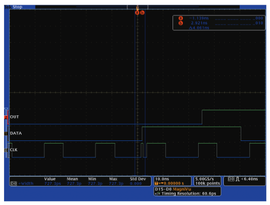
The clock positive pulse width is 7.455 ns and the trigger is configured to find non-conforming clock pulses less than 6.40 ns. Figure 17 shows the oscilloscope triggered on a 727.3 ps glitch on the clock signal just before the normal clock pulse. The analog channel is connected to the clock signal to obtain additional insight into this glitch and the MSO is started again. Figure 18 shows the oscilloscope triggered on a clock glitch and the MSO provides the analog insight of what is causing the glitch. The rising clock edge is non-monotonic. Using the cursors, the clock voltage is determined to be 2 V in the middle of the glitch and moving the cursor approximately 500 ps to the right, the clock voltage drops to 1.76 V. This voltage drop caused the logic state to change from logic high to low for a short time before the clock signal voltage continued to increase.

The 74F74 specification is 0.8 VIL maximum low-level input voltage and 2 VIH minimum high-level input voltage. A clock signal with slow rise time or non-monotonic operation between VIL and VIH can cause undefined D-Flip-Flop behavior. Based on this acquisition, the non-monotonic clock edge does not seem to be causing any problem. The non-monotonic clock edge was documented in the verification report and the next task is verifying the Q output operation.
The Q output should only change as a result of a change at the input and the change should only occur at the rising clock edge plus the D-Flip-Flop propagation delay. The clock has a fixed period of 20 ns. Therefore, the Q output should not have any pulses less than 20 ns wide because the Q output should only change at rising clock edges which are 20 ns apart. The MSO is configured to trigger on a Q output pulse width less than 19.2 ns.
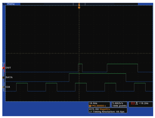
Figure 19 shows the MDO/MSO captured a Q output pulse width that is less than 19.2 ns. Notice that this Q output pulse width is less than the clock period. Analysis of the waveforms show that the D input is high when the rising clock edge occurred. The Q output low-to-high transition is correct but the following high-tolow transition is an error in the D-Flip-Flop operation because the transition is unrelated to a rising clock edge.
The analog channel is connected to the Q output to provide additional insight into the problem as shown in Figure 20. The Q output analog signal started to increase but shortly thereafter it decreased. Notice the Q output analog signal did not reach the normal analog logic high level before it dropped back down.
From past debugging experiences this may be a metastable glitch caused by a setup/hold timing violation of the D input in regards to the clock edge.
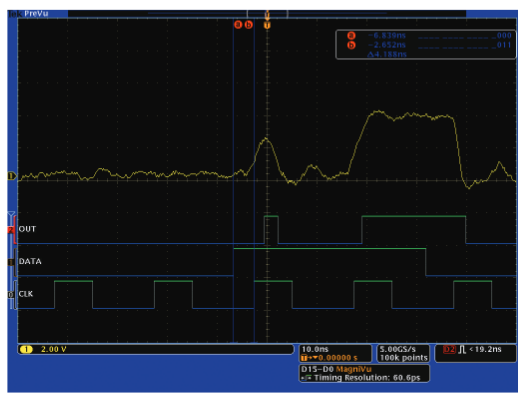
In Figure 20, the D input setup time is 4.188 ns as measured with the cursors. This setup time is twice as long as the 74F74's 2 ns minimum setup time specification. But, the 74F74 is not operating correctly with the D input changing 4.188 ns before the clock edge.
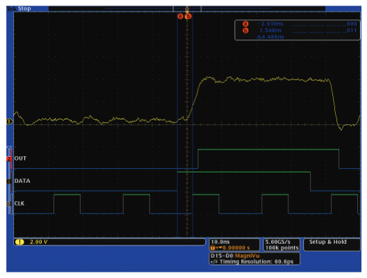
The oscilloscope triggering is changed to capture setup/hold violations to determine how much setup time is needed for this 74F74 to operate correctly. Figure 21 shows the Q output correctly working with a 4.488 ns setup time between the rising D input and the rising clock edge. Other acquisitions show the Q output having occasional glitches when the setup time is 4.188 ns or less.
Next, the D input is checked for setup/hold violations. MSO setup/hold triggering is configured for a 2 ns setup time and a 1 ns hold time to check for D input changes in the data valid window around the rising clock edge.

Figure 22 shows a serious D input setup/hold violation. Cursor 'a' is located at the minimum 2 ns setup time before the rising clock edge and cursor ‘b' is located at the minimum 1 ns hold time after the rising clock edge. The D input is required to be stable during this 3 ns data valid window around the rising clock edge. The D-Flip-Flop is not specified to work properly with the D input changing in data valid window.
At this point in the verification process there are three problems with the D-Flip-Flop operation and its signals. The first problem is a non-monotonic rising clock edge. The clock circuit needs to be redesigned to have a better rising edge. The second problem is the 74F74 is not correctly working with D input setup times of 2 ns to 4.188 ns. This may be related to the poor rising clock edge or the 74F74 is not meeting its specifications. The third problem is the D input setup/hold violation. The D input circuit needs to be redesigned so that it does not change during the clock edge setup/hold window.
Checking an Analog to Digital Converter for Missing Codes
In this example, the output range of a sensor's data acquisition system is verified with a fixed test ramp signal. The sensor data acquisition system is an analog signal conditioning circuit that feeds a 20 MS/s, 6-bit Analog to Digital Converter (ADC). The ADC 6-bit data bus is valid on the ADC falling clock edge. The test ramp signal at the acquisition system input should produce a range of ADC values from 00 to 3F hex.

The oscilloscope's analog channel is connected to the signal conditioning output which is also the ADC input. This provides a quick check of the signal conditioning output and ADC input signal. The digital channel zero is connected to the ADC clock output and digital channels one through six are connected to the ADC 6-bit data bus as shown in Figure 23. The oscilloscope is set to trigger on the rising edge of ADC input signal.

Figure 24 shows the MDO/MSO triggered on the rising edge of the input to the ADC. The unique front panel Wave Inspector® navigation controls are used to zoom to 20 X magnification around the trigger, allowing the parallel bus decode values to be easily seen. The ADC data is stable at the falling clock edge and the oscilloscope decodes the bus values at the falling edge of the clock. Therefore, the parallel bus updates at the falling clock edge when the ADC data is stable.
The MDO/MSO's powerful triggering finds signal faults and triggers on parallel or serial bus content to focus the acquisition on problem areas. However, once the data is acquired, triggering doesn't apply any more. Manually searching through long record lengths can be a frustrating and time-consuming process. A 10 Mpoint waveform record is over 10,000 full resolution screens of data. It takes over two hours and forty five minutes to scroll through a 10 Mpoint waveform at the rate of one full resolution screen per second. Whereas using Wave Inspector to search and mark a 10 Mpoint record 6-bit data bus acquisition takes about 30 seconds. Once the data has been found and marked, navigating between occurrences is as simple as pressing the front-panel Previous and Next arrow buttons. Searches are also available for trigger types such as edges, pulse widths, runt, setup/hold times, logic, rise/fall times and bus data values.
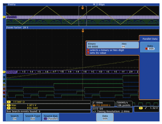
Figure 25 shows Wave Inspector searched the ADC parallel bus for 00 hex value which should be at each test ramp signal valley. But, no 00 hex values are found as indicated by the lack of white triangle search marks at the top of the display and as indicated by the search events readout showing zero at the bottom of the display. No 00 hex values means that the ADC did not see the analog input voltage that correspond to a 00 hex value. The acquisition system analog signal conditioning circuit did not correctly process the minimum peaks of the test ramp signal to match the minimum ADC input voltage in order for the ADC to produce a 00 hex output.

Figure 26 shows Wave Inspector searched for the maximum ADC output value of 3F hex. Wave Inspector's bus search found 18 events. These events are gathered in three groups of search marks which are located at the test ramp signal peaks. But each peak has multiple 3F hex values and not just one 3F hex value which should be at each test ramp signal peak.

Figure 27 shows the Wave Inspector right arrow navigation key was used to jump from the trigger position in Figure 26 to the first marked 3F event to the right of the trigger. Notice in the center of the display, the ADC output bus data is 37, 38, 39, 3A, 3B, 3C, 3D, 3E and six 3Fs hex values. The correct operation is one 3F hex value at the peak of the test ramp signal.
A clipped top of the test ramp signal at the ADC input could have produced multiple 3F hex values but the analog channel ADC input waveform looks good; it's not clipped or distorted at the test ramp signal peak. Rather, the multiple 3F hex values at the peak of the test ramp signal indicate that the analog signal exceeded the maximum ADC input voltage. The test ramp signal processed by the signal conditioning exceeds the maximum ADC input voltage and the processed signal does not reach the minimum ADC input voltage. To fix this problem the acquisition system signal conditioning offset and gain need to be adjusted. Notice the ADC input waveform maximum is 1.871 V and the minimum is 854.1 mV on the bottom left corner in Figure 27. The signal conditioning circuit offset and gain needs to lower both these values for correct operation.
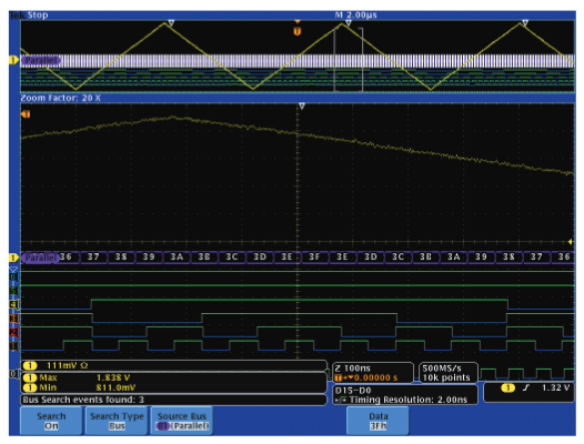
Figure 28 shows the acquisition system analog signal conditioning gain and offset are adjusted to provide a correctly processed test ramp signal to the ADC. After the signal conditioning adjustment the ADC input waveform maximum dropped from 1.871 V to 1.838 V. Now there is only one 3F hex value at each peak of the test ramp signal as expected. The maximum input of the ADC is correctly operating.
In Figure 28, the ADC conversion time is easily seen in this acquisition. The ADC conversion time is the time duration from the analog input peak to when the 3F hex value appears at the ADC outputs.

Figure 29 shows Wave Inspector searched for 00 hex value which should be at each ramp signal valley. Three 00 hex values were found, one at each valley of the test ramp signal as expected. Lastly, the Wave Inspector left navigation arrow key is used to jump to the first left mark 00 hex value event to check the ADC bus details at the test ramp valley as seen in Figure 29. The acquisition system is correctly operating with a count down to the minimum 00 hex value and a count up after the minimum. The bus values are saved to a .CSV file and are checked with Microsoft Excel for missing or duplicate values.
In this example, the digital channels were decoded into a clocked bus and Wave Inspector was used quickly to find, or not find, the maximum and minimum ADC bus values. The analog signal conditioning circuit was quickly identified as being the source of the problem.
Summary
The Tektronix MSO and MDO Series oscilloscopes are invaluable to designers who verify the complex interaction of digital, analog and software in their designs. Providing basic logic analyzer functionality with the ease-of-use of an oscilloscope, they feature comprehensive tools – powerful digital triggering, high resolution acquisition capability, and built-in analysis tools - to quickly verify and debug digital circuits.


