Why Test Power Supplies with an Oscilloscope?
Power supplies can be found in many different electronic devices, from children’s toys to computers and office equipment to industrial equipment. They are used to convert electrical power from one form to another for proper device operation. Common examples are AC-to-DC converters which change AC voltages into regulated DC voltages or DC-to-DC converters which convert battery power into required voltage levels.
Power supplies range from traditional linear supplies to high efficiency switch-mode power supplies (SMPS) designed for complex, dynamic operating environments. The load on a device can change dramatically from one instant to the next, and even a commodity switch-mode power supply must be able to withstand sudden peak loads that far exceed average operating levels. Engineers designing power supplies or the systems that use them need to understand their power supply’s behavior under conditions ranging from quiescent to worst-case.
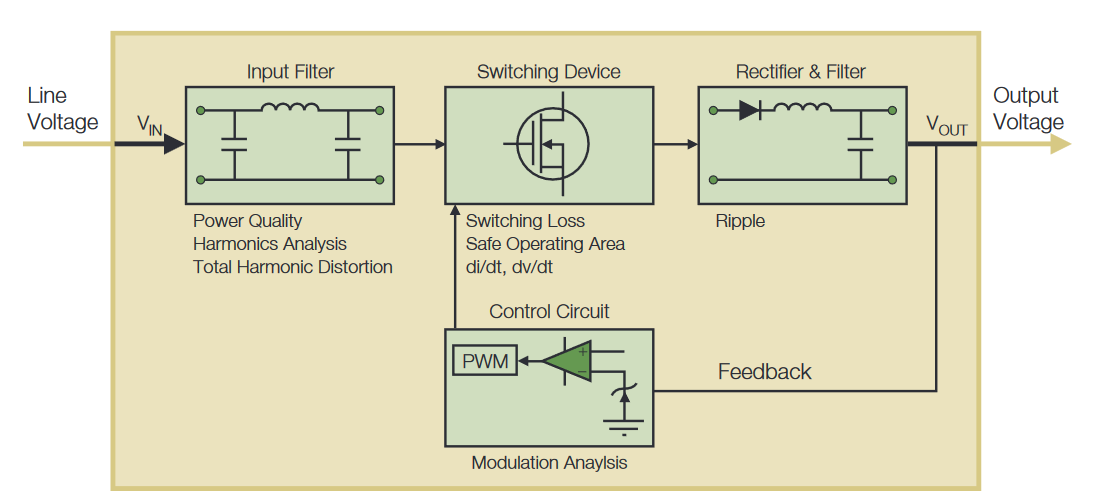
Historically, characterizing the behavior of a power supply meant taking static current and voltage measurements with a digital multimeter and performing painstaking calculations on a calculator or computer. Today, most engineers turn to the oscilloscope as their preferred power measurement tool.
This application note will describe common switch-mode power supply measurements, shown in Figure 1, using a Tektronix MDO4000 or MDO3000 Series oscilloscope. With the optional power measurement and analysis software, these oscilloscopes provide automated power measurements for fast analysis and simplified setup and deskew of probes for maximum accuracy.
5 Essential Steps for Accurate Power Supply Measurements
Ideally, a power supply would operate exactly as designed and modeled. In reality, components are imperfect; loads vary; line power may be distorted; environmental changes alter performance. Power supply design is further complicated by demands to increase performance, improve efficiency, reduce size and cut cost.
Given these design challenges, the measurement system must be setup correctly to accurately capture waveforms for analysis and troubleshooting. Important items to consider are:
- Oscilloscope Acquisition Modes
- Eliminating Skew Between Voltage and Current Probes
- Eliminating Probe Offset
- Current Probe Degauss
- Bandwidth Limiting Filters
Oscilloscope Acquisition Modes
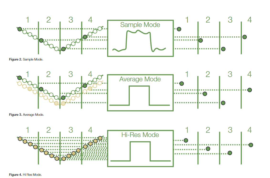
The oscilloscope’s acquisition modes control how electrical signals are sampled, processed, and displayed. The resulting waveform points are digital values that are stored in memory and displayed to construct the waveform. Most oscilloscopes support different acquisition modes, and the acquisition mode chosen may affect the accuracy of power measurements. It’s important to understand how acquisition modes function and the affect they will have on the waveform and ensuing power measurements.
Every oscilloscope offers Sample Mode, which is the simplest acquisition mode. As depicted in Figure 2, the oscilloscope creates a waveform point by saving one sample point during each waveform interval (waveform intervals are shown as 1, 2, 3, and 4 in the figure). Sample mode is suggested for measurements on non-repetitive signals that are acquired over multiple acquisitions such as ripple and noise analysis.
Another acquisition mode offered by most oscilloscope manufacturers is Average Mode. In Average Mode, the oscilloscope saves one sample point during each waveform interval as in sample mode. However, in Average Mode, corresponding waveform points from consecutive acquisitions are then averaged together to produce the final displayed waveform as depicted in Figure 3. Average Mode reduces noise, but requires a repetitive signal. Average Mode is especially useful when performing harmonics analysis or power quality analysis measurements such as true power, reactive power and apparent power.
Tektronix also offers Hi Res Mode. In this mode, multiple consecutive samples taken within one waveform interval are averaged together to produce one waveform point from a single acquisition as shown in Figure 4. The result is a decrease in bandwidth and therefore noise, and an improvement in vertical resolution for low-speed signals. Hi Res is especially useful for conducting modulation analysis when powering up a supply and acquiring data in a single acquisition. Hi Res may improve the accuracy of measurements such as switching loss, which are based on mathematically calculated values like instantaneous power.
Eliminating Skew between Voltage and Current Probes
To make power measurements with a digital oscilloscope, it is necessary to measure voltage across and current through the device under test. This task requires two separate probes: a voltage probe (often a high voltage differential probe) and a current probe. Each voltage and current probe has its own characteristic propagation delay and the edges produced in these waveforms more than likely will not be automatically aligned. The difference in the delays between the current probe and the voltage probe, known as skew, causes inaccurate amplitude and timing measurements. It is important to understand the impact of the probe’s propagation delay on maximum peak power and area measurements as power is the product of voltage and current. If the voltage and current signals are not perfectly aligned, results will be incorrect.
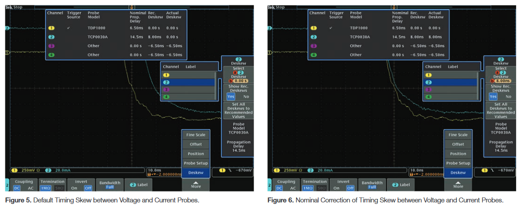
Tektronix MDO4000 and MDO3000 Series oscilloscopes offer a "Deskew" feature to remove the skew between the probes. When the Deskew menu is selected, an information box is displayed that describes the Probe Model, Nominal Propagation Delay, Recommended Deskew and Actual Deskew for each channel. The voltage and current waveforms in Figure 5 have approximately 8 ns of skew and the propagation delay for each probe is shown in the information box. The TDP1000 (Tektronix differential voltage probe) has a nominal propagation delay of 6.5 ns whereas the TCP0030A (Tektronix current probe) has a nominal propagation delay of 14.5 ns. The difference in propagation delays is 8 ns.
Correcting for the skew between the probes is as simple as selecting the "Set all deskews to recommended values" side bezel button as shown in Figure 6. Choosing this option adjusts the probes’ "Actual Deskew" values to the "Recommended Deskew" values. The "Recommended Deskew" value is based upon the probe’s nominal propagation delay which is stored in the probe’s internal memory, assuming the probe is TekVPI® enabled or generally supports automated probe deskew.
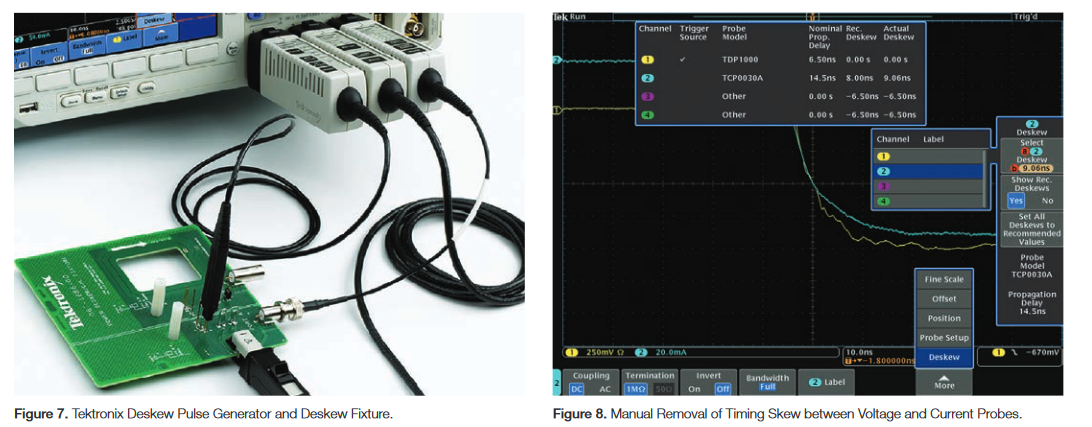
Selecting "Set all deskews to recommended values" accounts for the probe's nominal propagation delay differences which will come very close to deskewing them correctly, but still may not precisely align the waveforms. In order to precisely align the waveforms for greatest measurement accuracy, the TEK-DPG (Deskew Pulse Generator) and deskew fixture are required.
The TEK-DPG provides a source signal to the Power Measurement Deskew Fixture (Tektronix part number 067-1686-XX) as shown in Figure 7. With the probes connected to the deskew fixture, the “Actual Deskew” may be manually dialed-in to change the deskew value to precisely align the waveforms. Figure 8 depicts that the TDP1000 probe’s "Actual Deskew" value has been adjusted 680 ps from 6.5 ns to 9.06 ns for maximum accuracy
Eliminating Probe Offset
Differential probes tend to have a slight voltage offset. This offset can affect accuracy and must be removed before proceeding with measurements. Most differential voltage probes have built-in DC offset adjustment controls, which makes offset removal a relatively simple procedure.
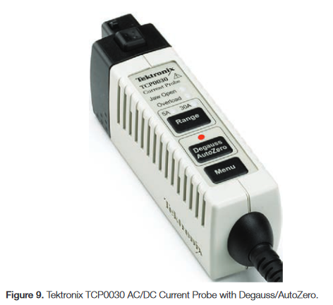
Current probes may also need to be adjusted before making measurements. Current probe offset adjustments are made by nulling the DC balance to a mean value of 0 amperes or as close as possible. TekVPI-enabled probes, such as the TCP0030A AC/DC current probe, have an automatic Degauss/AutoZero procedure built in that’s as simple as pressing a button on the probe compensation box.
Degauss
A current probe should also include an easy to use degaussing feature. Degauss removes any residual DC flux in the core of the transformer, which may be caused by a large amount of input current. This residual flux results in an output offset error that should be removed to increase the accuracy of the measurements being made.
Tektronix TekVPI current probes offer a Degauss warning indicator that alerts the user to perform a degauss operation.Since current probes may have significant drift over time which affects measurement accuracy, a degauss warning indicator is a useful feature.
Bandwidth Limiting Filters
Limiting the oscilloscope’s bandwidth removes noise or unwanted high frequency content from the displayed waveform, resulting in a cleaner signal. The MDO4000 and MDO3000 Series offers built-in bandwidth limiting filters, as shown in Figure 10. In some cases, the probe may also be equipped with bandwidth limiting filters.
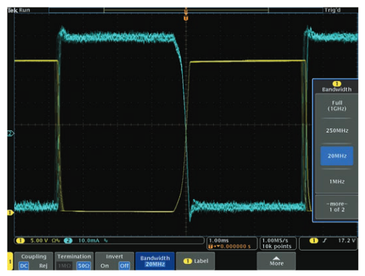
The user should be careful when using these filters, as high frequency content contained in nth order harmonics may be removed from the measurement. For example, if measuring a 1 MHz signal, and evaluating out to the 40th harmonic, at least 40 MHz of system bandwidth is required. Setting the bandwidth limiting filter to 20 MHz, which is an available option in the example shown in Figure 10, would eliminate the frequency content required for this measurement.
How to Test Your Power Supply: From Input to Output
Once the measurement system is properly set up, the task of performing power measurements can begin. The common power measurements can be divided into three categories: input analysis, switching device analysis and output analysis.
Input Analysis
Real-world electrical power lines never supply ideal sine waves, and there is always some distortion and impurity on the line. A switching power supply presents a non-linear load to the source. Because of this, the voltage and current waveforms are not identical. Current is drawn for some portion of the input cycle, causing the generation of harmonics on the input current waveform. Key measurements for analyzing the input of the power supply are:
- Harmonics
- Power Quality
Harmonics
Switching power supplies tend to generate predominantly odd-order harmonics, which can find their way back into the power grid. The effect is cumulative, and as more and more switching supplies are connected to the grid (for example, as an office adds more desktop computers), the total percentage of harmonic distortion returned to the grid can rise. Since this distortion causes heat buildup in the cabling and transformers of the power grid, it’s necessary to minimize harmonics. Regulatory standards such as IEC61000-3-2 are in place to oversee power quality from a particular non-linear load.
Determining the effects of these distortions is an important part of power engineering, and the benefits of using an oscilloscope rather than a multimeter are significant. The measurement system must be able to capture harmonic components up to the 50th harmonic of the fundamental. Power line frequency is usually 50 Hz or 60 Hz; though for some military and avionics applications, the line frequency may be 400 Hz. It should also be noted that signal aberrations may contain spectral components with even higher frequency components. With the high sampling rate of modern oscilloscopes, fast-changing events may be captured with great detail (resolution). In contrast, conventional power meters can overlook signal details due to their relatively slow response time.
Performing harmonics analysis is as easy as taking an ordinary waveform measurement. Since the signal in this case is a repeating periodic waveform, it’s a simple matter to trigger and display it. At least five cycles should be displayed to ensure good frequency resolution, and the vertical scale should be set such that the signal occupies as many vertical divisions on the display as possible for best measurement accuracy.
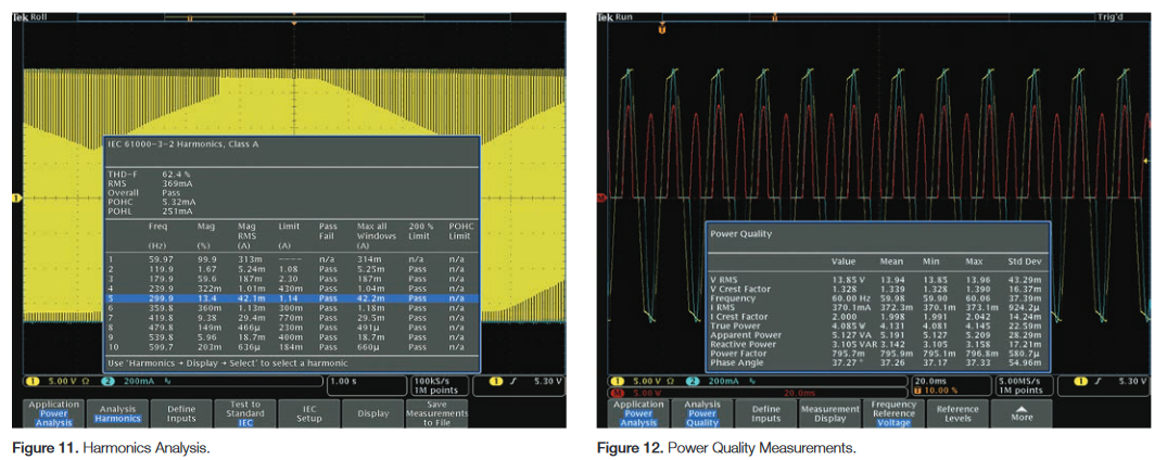
Figure 11 shows the result of a harmonic analysis on a power supply’s load current. In the Display menu, measurements on a specific harmonic may be selected. In this example, the fifth harmonic was selected. Users may choose to view the results as a table or a graph and can select whether to view “All, Odd, or Even” harmonics. Harmonics data may be saved as a CSV file to a USB storage device. Total Harmonics Distortion (THD) values relative to the fundamental and RMS value are also displayed. These measurements are useful in analyzing compliance to standards such as IEC61000-3-2 and MILSTD-1399 that are included in the power application software.
Power Quality
Power quality does not depend on the electricity producer alone. It also depends on the power supply and the end-user’s load. The power quality characteristics at the power supply define the "health" of the power supply and determine the effects of distortions caused by non-linear loads. As shown in Figure 12, the power application software provides a results table with the following automatic measurements: VRMS and IRMS, Voltage and Current Crest Factors, True Power, Reactive Power, Apparent Power, and Power Factor.
Switching Device Analysis The prevailing DC power supply architecture in most modern systems is the SMPS because of its ability to efficiently handle changing input voltages and loads. The SMPS minimizes the use of lossy components such as resistors and linear-mode transistors, and emphasizes components that are (ideally) lossless. SMPS devices also include a control section containing elements such as pulse-widthmodulated regulators, pulse-rate-modulated regulators, and feedback loops.
SMPS technology rests on power semiconductor switching devices such as Metal Oxide Semiconductor Field Effect Transistors (MOSFET) and Insulated Gate Bipolar Transistors (IGBT). These devices offer fast switching times and are able to withstand erratic voltage spikes. Additionally, transistors dissipate very little power in either the On or Off states, achieving high efficiency with low heat dissipation. For the most part, the switching device determines the overall performance of an SMPS. Key measurements for switching devices include:
- Switching Loss
- Safe Operating Area
- Slew Rate
Switching Loss
Transistor switch circuits typically dissipate the most energy during transitions because circuit parasitics prevent the devices from switching instantaneously. The energy lost in a switching device, such as MOSFET or IGBT as it transitions from an OFF to ON state is defined as Turn-on loss. Similarly, Turn-off loss is the energy lost when the switching device transitions from an ON to OFF state. Transistor circuits lose energy during switching due to dissipative elements in the parasitic capacitance and inductance and charge stored in the diode. A proper analysis of these losses is essential to characterize the supply and gauge its efficiency.
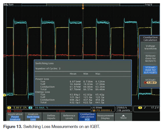
The switching loss measurements as shown in Figure 13 are made on complete cycles within the selected region of the acquisition (by default, the entire waveform) and the statistics of those measurements are accumulated across the acquisition, but not between acquisitions.
A major challenge in measuring Turn-on and Turn-off losses is that the losses occur over very short time periods, while the losses during the remainder of the switching cycle are minimal. This requires that the timing between the voltage and current waveforms is very precise, that measurement system offsets are minimized, and that the measurement’s dynamic range is adequate to accurately measure the On and Off voltages and currents. As discussed earlier, the probe offsets must be nulled out, the current probe must be degaussed to remove any residual DC flux in the probe, and the skew between channels must be minimized.
The other major challenge is the high dynamic range required for accurate switching loss measurements. The voltage across the switching device changes dramatically between the On and Off states, making it difficult to accurately measure both states in a single acquisition. There are three ways to determine the correct values with the MDO4000 and MDO3000 Series:
- Measure the voltage drop across the switching device during conduction. Because this voltage is typically very small compared with the voltage across the switching device when it is not conducting, it is generally not possible to accurately measure both voltages at the same vertical setting on the oscilloscope.
- Provide the RDS(on) value (best model for MOSFETs) based on the device data sheet. This value is the expected on-resistance between the drain and source of the device when it is conducting.
- Provide the VCE(sat) value (best model for BJTs and IGBTs) based on the device data sheet. This is the expected saturation voltage from the collector to the emitter of the device when it is saturated.
Safe Operating Area (SOA)
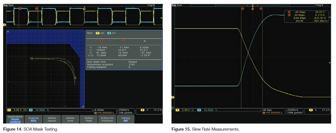
The Safe Operating Area (SOA) of a transistor defines the conditions over which the device can operate without damage; specifically how much current can run through the transistor at a given voltage. Exceeding these limits may cause the transistor to fail. The SOA is a graphical test technique which accounts for limitations of the switching device such as maximum voltage, maximum current, and maximum power, and assures that the switching device is operating within specified limits.
The switching device manufacturer’s data sheet summarizes certain constraints on the switching device. The object is to ensure that the switching device will tolerate the operational boundaries that the power supply must deal with in its enduser environment. SOA test variables may include various load scenarios, operating temperature variations, high and low line input voltages, and more. As depicted in Figure 14, a userdefinable mask is created to ensure that the switching device adheres to defined tolerances in regard to voltage, current, and power. Mask violations are reported as failures in the power application.
Slew Rate
To verify that the switching device is operating at maximum efficiency, the slew rate of the voltage and current signals is measured to verify that the circuit is operating within specifications. As shown in Figure 15, the oscilloscope is used to determine the slew rate of the switching signals by using measurement cursors, simplifying gate drive characterization and switch dv/dt or di/dt calculations.
Output Analysis
Ideally, the output of a DC power supply should not have any switching harmonics or other non-ideal noise components. Realistically, that is not possible. Output analysis measurements are essential to determine the effects of variations in input voltage or load on the output voltage. These measurements include:
- Modulation Analysis
- Ripple
Modulation Analysis
The digital phosphor acquisition technology of the MDO4000 and MDO3000 Series offers unique advantages when troubleshooting designs, especially when identifying excessive modulation effects in a switching power supply. These oscilloscopes have greater than 270,000 wfm/s maximum waveform capture rate, which is many times higher than that of a typical digital storage oscilloscope (DSO). This provides two advantages when investigating modulation effects. First, the oscilloscope is active more of the time, and less time is spent processing waveforms for display. Thus the oscilloscope has significantly more chances to capture the modulation. Second, the digital phosphor display makes it easier to see the modulated waveforms in real time. The display intensifies the areas where the signal trace crosses most frequently, much like an analog scope. The modulation is dimmer than the main waveform that repeats continuously, making it easier to see.
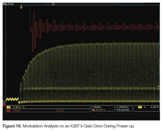
Measuring modulation effects with a Tektronix oscilloscope is also easy. Figure 16 shows the pulse width modulated signal controlling the output of a current mode control loop on a power supply. Modulation is important in a feedback system to control the loop. However, too much modulation can cause the loop to become unstable. The red waveform is a math waveform, showing the trend in cycle-to-cycle pulse width measurements made on an IGBT gate drive signal as the power supply’s oscillator starts up. Since the math waveform represents pulse width measurement values (with units of time), variations in pulse widths may be measured using cursors. The math values represent the trends in the selected modulation measurement across the acquired waveform. In this case, it represents the response of the oscillator’s control loop during startup. This modulation analysis could also be used to measure the response of the power supply’s control loop to a change in input voltage (“line regulation”) or a change in load (“load regulation”).
Ripple
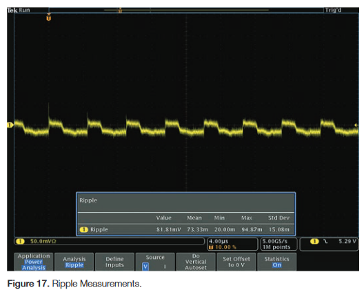
Ripple is the AC voltage that is superimposed onto the DC output of a power supply. It is expressed as a percentage of the normal output voltage or as peak-to-peak volts. Linear power supplies usually see a ripple that is close to twice the line frequency (~120 Hz), whereas switching power supplies may see a switching ripple in the hundreds of kHz.
Simplify Your Power Supply Testing with Tektronix
The power supply is integral to virtually every type of linepowered and battery-operated electronic product, and the switch-mode power supply (SMPS) has become the dominant architecture in many applications. A single switch-mode power supply’s performance or its failure can affect the fate of a large, costly system.
To ensure the reliability, stability, performance, and compliance of an emerging SMPS design, the design engineer must perform many complex power measurements. The Tektronix MDO4000 or MDO3000 Series oscilloscopes with a power analysis application module dramatically simplifies the analysis of power supplies. Automated power measurements such as harmonics, power quality, switching loss, safe operating area, slew rate, modulation and ripple ensure fast analysis while simplified setup and deskew of probes provides maximum accuracy
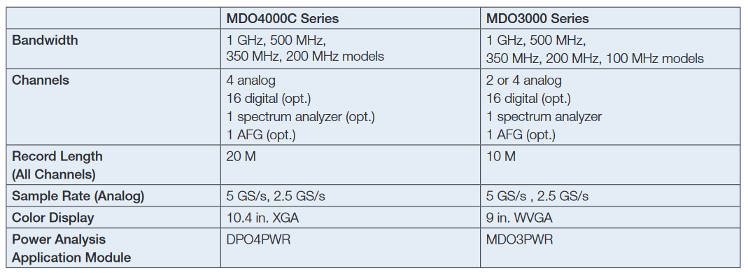
Which oscilloscope is right for you?
Tektronix Bench Oscilloscopes offer a range of models to meet your needs and your budget
Find the right instrument to power your next project.
Have questions? Get personalized advice for your specific application.

