Overview
The MIPI® Alliance has established specifications for standard interfaces used in mobile electronics. While the MIPI® standards define several physical layers, the MIPI M-PHY standard presents some significant challenges for oscilloscope measurements and probing. The challenges include strict requirements such as bus termination and input return loss. Other challenges include minimizing common mode loading on the device under test (DUT) with wide bandwidth for signal fidelity measurements as well as low noise and high sensitivity. Tektronix has oscilloscope probing solutions that are uniquely positioned to meet the needs of engineers testing conformance of MIPI M-PHY transmitters (M-TX). This application note will review the requirements of the M-PHY standard that relate to oscilloscope probing, discuss tests required in the M-PHY Physical Layer Conformance Test Suite (CTS), and provide practical examples of M-PHY probing with currently available oscilloscopes and probes.
MIPI M-PHY Specification Details
Termination
The MIPI M-PHY standard supports different speed modes, high-speed (HS) and lower speed PWM and SYS modes. In each of these speed modes there are different data rates or GEARs. In HS mode, the official specification is released for GEAR 1 (~1.5 Gb/s), GEAR 2 (~2.9 Gb/s), and GEAR 3 (~5.8 Gb/s). To increase the likelihood of MIPI M-PHY designs from different manufacturers working when used together, the MIPI Alliance recommends that designs be tested against the M-PHY Physical Layer Conformance Test Suite (CTS). With the development of the GEAR 4 (~11.6 Gb/s) specification proceeding, testing conformance is becoming more of a challenge.
The voltage measurements specified in the M-PHY standard assume that the bus has a known reference load (RREF in Figure 1) that is connected between the positive (TXDP) and negative (TXDN) outputs of the M-PHY transmitter (M-TX).
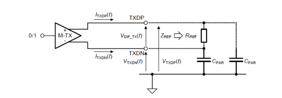
The reference load varies according to the state of the line, which can be either not terminated (NT) or resistively terminated (RT). When the line is operating in its NT mode, RREF_NT is specified as a minimum impedance of 10kΩ between the TXDP and TXDN pins. The not terminated mode is most often used for low-speed communications, since driving a high speed signal into a high impedance termination, can be very challenging for all but the shortest transmission lines.
When needed, the NT bus mode can be measured using a high impedance active or differential probe. These oscilloscope probes can meet or exceed the specification with 10kΩ or higher impedance for signal frequencies that are less than a few MHz. For the resistively terminated mode of the line, the M-PHY standard defines RREF_RT as a floating 100Ω impedance across the TXDP and TXDN pins. For the RT state of the bus probes and scopes that have 50Ω input impedance are available. Measuring the line in high-speed, RT mode with an oscilloscope requires that either the scope or its probe appear to be as close to the desired 100Ω differential termination as possible.
When the M-PHY line is operating in high speed mode (HS-MODE), it will most likely be terminated unless the transmission distance is very short compared to the wavelength of the signals to minimize reflections and to mimic a receiver with low input impedance.
In addition, conformance testing for HS-MODE is typically only defined for the RT case. The current M-PHY CTS only specifies high speed tests in RT mode, stating that high speed data measurements such as jitter on non-terminated signals are typically not practical or even possible. The M-PHY standard also notes this difficulty in section 5, which states, "… jitter in non-terminated mode cannot be practically measured."2
A floating 100Ω termination is the ideal, but difficult to realize in practice due to parasitic elements in a design. Therefore, several alternative approaches have been proposed to achieve a nominal 100Ω differential termination along with sufficient return loss and high common mode impedance that minimizes DC and AC current draw on the transmitter. The table below compares the ideal 100Ω termination to four practical alternatives.
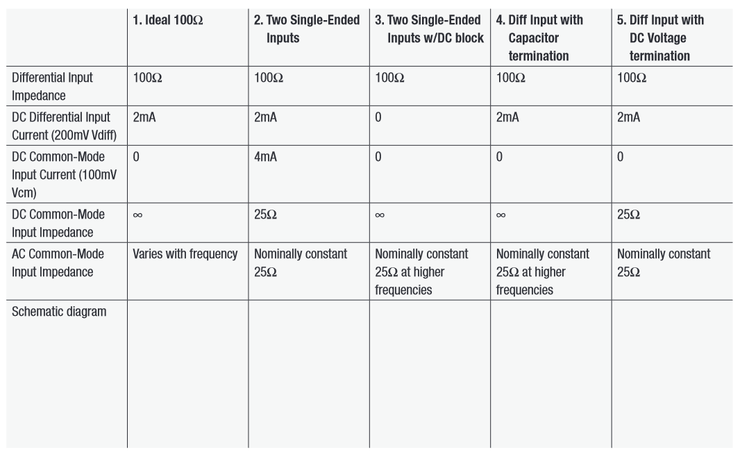
All the alternatives meet the requirement for 100Ω differential input impedance. Where they differ is in common mode current draw and CM input impedance. Since the ideal floating 100Ω cannot be achieved with real components, an engineer testing M-PHY HS signaling must decide on one of the practical alternatives. Each alternative has its own pluses and minuses. Common mode current flow and common mode input impedance are two areas where the alternatives differ significantly. Notice that a floating 100Ω termination will have a common-mode impedance that varies widely over M-PHY’s frequency range due to parasitic elements. All the alternate termination schemes have the differential properties of the ideal 100Ω, but exhibit other undesirable characteristics like 25Ω common-mode input impedance at high frequency. Common-mode performance is discussed in more detail below.
Connecting the M-TX line directly to two channels of a scope is equivalent to the two single-ended inputs approach (alternative #2). This alternative has the disadvantage of drawing common-mode current from the transmitter, which may cause problems for the transmitter. In alternative #3, adding DC blocking capacitors to the dual single-ended termination addresses the DC commonmode current, but the capacitors must be chosen very carefully to ensure the termination meets the M-PHY return loss specification. Also, using blocking caps prevents DC measurements on the M-TX required by the CTS.
The two final alternatives mimic the ideal 100Ω resistor by drawing no DC common-mode current, but have low common-mode impedance (25Ω). These approaches, however, allow for the common-mode impedance to be controlled better than the floating 100Ω termination. If the capacitor (alternative #4, Cterm) used with the termination is large enough, the AC common mode impedance will be nominally constant at 25Ω. 100nF is needed for this to start at 1MHz.
The DC voltage termination (alternative #5, Vterm) capability includes DC sources inside the probe or scope that provide adjustable DC termination reference levels. Setting the Vterm level to the M-TX’s common-mode voltage results in no common mode (CM) current and eliminates the need for DC-blocks or bias-tees. Unlike a DC block, however, the signal DC voltage is still present at the probe or scope input and can be measured. Using Vterm minimizes the DC loading. By setting the Termination Voltage equal to the DC bias voltage of the input signal, the probe DC loading is nulled out.
Return Loss
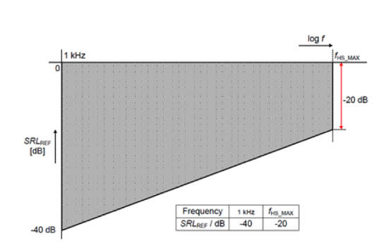
The termination of the M-PHY bus at GEAR 3 speeds and higher is further specified by the return loss for the reference load ZREF_RT according to the figure and values in Figure 2. High return loss limits unwanted reflections from the line that can impact the quality of the measurements.
If the termination for the bus is provided by a probe, fixture, or a scope, their input return loss must meet this requirement. Some of the issues that can prevent a system from meeting the return loss requirement include capacitive loading across the 100Ω termination. The return loss specification sets some practical limits on the amount of series and parallel loading allowed. Table 2 lists the limits for these values for GEAR 3.

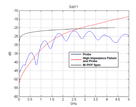
These constraints can limit the choices for the line termination with a probe or scope. Figure 3 shows two termination approaches and their input return loss. The first one is a probe with 50Ω differential inputs (blue trace). The second is a high impedance differential probe attached to a 100Ω termination fixture (red trace). In this example, the probe shown in blue meets the M-PHY specification by remaining below the M-PHY specified limit line. The high impedance fixture + probe do not meet the spec as they exceed the limit at 2.7 GHz and above.
Measurement Sensitivity/Low Noise
Now that we have established the input termination and return loss specifications can be met using a probe and scope, the discussion will switch to the required measurements and their impact on the probe choice. Additional requirements in the M-PHY specification and CTS make testing the transmitter challenging. M-PHY transmitter tests that cover HS-MODE GEARs 1-3 include: intra-lane skew, pulse width, common mode, total and deterministic jitter. M-PHY transmitters can support different drive strengths in an effort to save power. The M-TX measurements are defined in the CTS with the M-TX running in both Large Amplitude (LA) and Small Amplitude (SA) modes. M-PHY’s low amplitude signaling and the need to measure jitter require that the probe and scope acquire low peak-to-peak voltage signals with fast edges.
In the power saving Small Amplitude mode, the M-PHY transmitter’s output peak to peak voltage is reduced to a maximum of 280 mV. Slew rates must be controlled in the M-TX to reduce EMI noise. However, minimizing jitter at high data rates requires an edge speed that is a fraction of a UI. Even when the M-TX is running in large amplitude mode, the amplitude of M-PHY signals is relatively small, 0.5Vpp. The table below lists the range of the minimum and maximum voltage levels for the outputs (TXDP and TXDN) operating in LA and SA modes.

Acquiring these low amplitude signals requires a high bandwidth measurement system with high sensitivity. Also, low additive noise within the probe and scope are key to making accurate measurements on these low amplitudes.
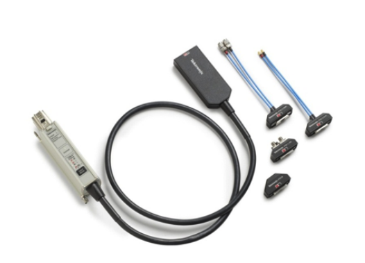
A key to determining the usability of a probe for low amplitude signals is checking the probe’s noise specifications and its minimum attenuation value. Probes with high input impedance, typically attenuate the signal at their inputs in order to minimize circuit loading. High impedance probes attenuate the signal as it enters the probe. Using a high attenuation factor, these probes limit their loading on the device under test. Probe loading is not an issue with M-PHY in HS-MODE as it is expected that the bus will be driving a low impedance (100Ω) differential load in RT mode. The attenuation factor of the probe works against the goal of having a low noise input by reducing the signal-to-noise ratio of the measurement by a factor equal to the probe’s attenuation value.
To see the difference probe attenuation can make, we will compare two probe types in example measurements of 5.8 Gb/s, low amplitude (~200 mVpp) data signals. The first probe used has 50Ω, SMA-style inputs.
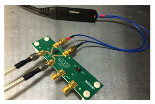
Since the loading of the probe is not a concern, the SMAstyle probe with 50Ω inputs can be used to acquire the M-PHY TX signals. The second probe we will evaluate is a high impedance differential probe with a 100Ω termination fixture attached to the TX outputs and then attached to the probe inputs.
The SMA-style probes have the advantage over high impedance probes that their attenuation settings are much lower than the high impedance probes. For example, a Tektronix P7633 SMA-style probe can be set to have an attenuation factor of 1X or even <'1X for small amplitude signals. A high impedance probe with similar bandwidth performance has a minimum attenuation of 5X. With lower attenuation in the probe, the measurement results are cleaner with lower noise. This difference can be seen in an eye diagram. Figures 6 and 7 compare the same 5.8 Gb/s, 200mVpp signal acquired with a Tek P7633 probe (50Ω, low attenuation) and a Tek P7520A high impedance probe (100kΩ DC impedance, minimum 5X attenuation). Both probes were bandwidth limited to 20 GHz.
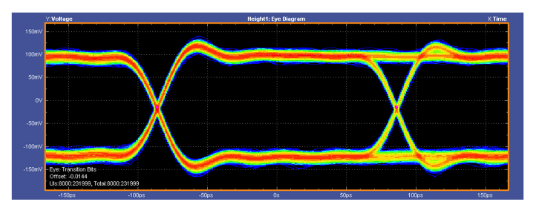
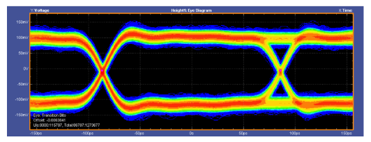

You can see the difference in noise between these two eye diagrams by comparing the "fuzz" in each of the two. The data acquired with the P7633 SMA-style probe is cleaner and less fuzzy than the eye diagram acquired using the P7520A high impedance probe. Measured parameters shown in the table for both eye diagrams confirm that the P7633 eye diagram is more "open" than the P7520A eye diagram. For example the eye opening measurement reduced by 18% when using the high impedance probe due to its higher noise.
Other high impedance probes show similar noise levels in the eye diagram due to their high attenuation values.
Oscilloscope and probe noise performance are critical for accurately measuring the characteristics of the M-PHY signals. Without a low noise floor, other capabilities of the scope and probe are useless since the noise can hide key characteristics of the signal. With M-PHY, the noise performance of the measuring system is critical because of tight amplitude requirements defined in the specification. Remember in the Small Amplitude (SA) mode of operation, the M-TX peak-to-peak output voltage ranges from 160mV to 280 mV. The difference between logic levels is relatively small if the scope and probe do not have low noise and do not have sufficient sensitivity (20-30 mV/div, 200-300 mV full-scale).

Beware of scope specifications that increase their sensitivity by zooming the signal display when the limit of the frontend hardware has been reached. Zooming on a signal only increases the visibility of a signal it does not increase the sensitivity. The zoom operations also increase the noise shown on screen.
The M-PHY specification for the minimum TX rise time (20%/80%) is 0.1*UI, equivalent to 17.2ps in GEAR 3. However, the practical rise time of the M-TX signal at the measurement point is limited by capacitance in the package and the circuit board traces. Although the actual capacitance of a device may not be known, if its capacitance is as high as the maximum specified value for CPIN_RX of 1.5pF4 , then the rise time for GEAR 3 signals will be increased from 0.1*UI to a value closer to 0.4*UI (70ps).
Ideally, a probe and scope should have very low capacitance and a rise time 3X faster than the signal being measured. Using the rise time value for GEAR 3, it is difficult to find a scope or probe that has a rise time 3X faster than 17.2ps (0.1*UI). It is an easier task to find a probe with a rise time that is 3X faster than 70ps (0.4*UI). Here are a few examples of probes and their rise time specifications.
Since in practical terms, the signal’s rise time at the probe point will likely be much slower than 17.2 ps. How can an engineer verify that their TX output does not exceed the limit of 0.1*UI specified in the M-PHY specification? The CTS recommends making the rise time measurement and then using a de-embedding process to remove any signal loss from PCB traces, cables and connectors. Using deembedding, it is possible to determine what the rise time of the signal is at the M-TX pin and determine whether or not the TX meets the requirements of the standard.
Common-mode Signals
AC and DC common mode output from the M-PHY TX is an undesirable source of EMI. Therefore, measuring the AC and DC common mode (CM) signals at the M-TX outputs are a part of the M-PHY CTS measurements. The floating 100Ω termination of the line is intended to provide a termination with no path to ground where the common mode current can flow. As was discussed earlier this ideal termination is not possible with today’s PCB materials and components.
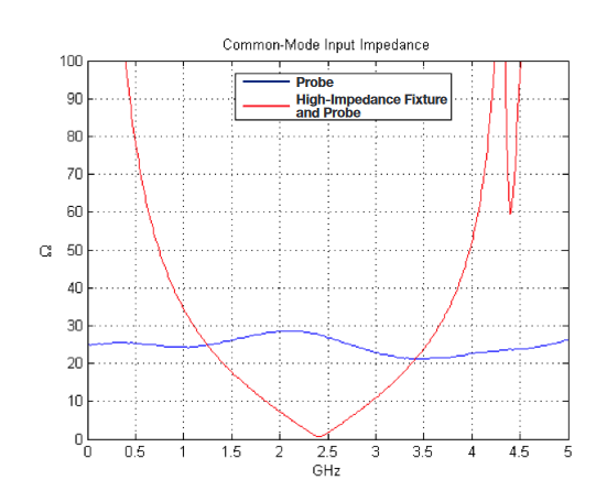
All practical termination approaches will have commonmode loading at M-PHY frequencies. This loading attenuates the common-mode signal level and must be de-embedded for accurate CM measurements. The more consistent the common-mode load, the easier it is to de-embed the loading effect. The plot below shows two examples of common mode input impedance for the SMA probe and high impedance probe + fixture compared earlier over the frequency range defined by M-PHY GEAR 3 data rates.
The blue line, in Figure 8, shows a common mode impedance that does not vary significantly above or below 25Ω from DC to 5 GHz (the M-PHY frequency range of interest). Whereas the second probe (red trace) has impedance that varies widely from DC to 5 GHz. Although DC current will flow in both cases, the de-embedding of the probe loading for a common mode measurement with the probe shown in the blue trace is simply a scaling operation. Considering the voltage divider ratio of the TX’s source impedance and the 25Ω CM input impedance of the probe, the measured common mode voltage using this probe should be multiplied by 2. The common mode deembedding task for the high impedance fixture is a more complex operation.

Measurement Requirements Summary
The table below summarizes the requirements for measurement equipment used to test conformance of an M-PHY transmitter running in high-speed mode.
The MIPI M-PHY standard presents significant challenges for oscilloscopes and probing. These challenges result in stringent requirements for HS-MODE measurements. SMA style probes with 50Ω inputs have been shown to yield superior results compared to high impedance probe approaches, particularly for HS-GEAR 3 speeds. Therefore, the newest version of the M-PHY CTS has been updated to list support for "SMA probe" type probing solutions. Tek SMA probes like the P7633 are unique in that they can meet the requirements of M-PHY testing and introduce lower noise than other oscilloscope probes.
Recommendation
The Tektronix MSO/DPO70000DX Oscilloscopes and SMA P7600 Series TriMode Probes are Tektronix’ recommended equipment for M-PHY HS GEAR3 and higher transmitter measurements. This equipment meets the M-PHY requirements. They also provide convenient and consistent bus termination for HS measurements with low noise and high sensitivity. When testing conformance of lower speed, NT M-PHY signaling, such as PWM, lower bandwidth probes with high input impedance level are sufficient. Tektronix’ differential probes such as the P7300 series Z-Active™ probes provide a high impedance input along with a range of bandwidth options from 4 to 13 GHz for these conformance measurements.
Two Probes vs. One TriMode Probe

Tektronix offers a unique capability on our fastest differential probes. The TriMode feature allows the measurement of differential, single-ended, and common mode signals with a single probe connection to the TX_DP and TX_DN outputs.
Using a TriMode probe, an engineer can more efficiently make differential and single-ended measurements on the M-PHY TX. Plus the common mode setting of the TriMode probe, the TX’s common mode output voltage can be directly measured.
When looking for intra-lane skew between the TX_P and TX_N signals, the common mode setting of the TriMode probe can be used to recognize any lane to lane skew as shown in the figure above.5
Any skew between the 2 signals will show as a glitch or a change in the common mode signal. Some skew measurements are still specified to use two probes or two scope channels, so one probe can’t do it all. However, for a majority of the M-TX HS-MODE measurements, a TriMode probe can make the testing easier.
The TriMode capability is available on Tektronix’ P7600 and P7500 series probes.


