연락처
텍트로닉스 담당자와 실시간 상담 6:00am-4:30pm PST에 이용 가능
전화
전화 문의
9:00am-6:00PM KST에 이용 가능
다운로드
매뉴얼, 데이터 시트, 소프트웨어 등을 다운로드할 수 있습니다.
피드백
Electrical Sampling Modules
80E02
이 데이터 시트의 제품은 텍트로닉스에서 더 이상 판매하지 않습니다.
리퍼브 테스트 장비에 대한 Tektronix Encore를 확인하십시오.
이러한 제품에 대한 지원 및 보증 상태를 살펴보십시오.

Features & Benefits
All Modules
- Up to 70 GHz Bandwidth and 5 ps Measured Rise Time (10 - 90%)
- Lowest Noise for Analysis – 450 μVRMS at 60 GHz, 300 μVRMS at 30 GHz
- Remote Samplers*1 Enable Location of Sampler Near DUT and Ensure Best Signal Fidelity
- Independent Sampler Deskew Ensures Easy Fixture and Probe De-embedding
- Precision Microwave Connectors (3.5 mm, 2.92 mm, 2.4 mm and 1.85 mm)
- Probe Support
TDR Modules
- 15 ps Reflected True Differential Fully Integrated TDR Rise Time (12 ps Incident) and Feature Resolution Below 1 mm
- Efficient, Accurate, Easy to use, and Cost Effective S-parameters up to 50 GHz
Applications
- Impedance Characterization and S-parameter Measurements for Serial Data Applications
- Advanced Jitter, Noise and BER Analysis
- Channel and Eye Diagram Simulation and Measurement-based Spice Modeling
80E02
- Device Characterization, Transmission Quality, Waveform Parameters
- Low Signal Measurements
Sampling Modules: 80E02
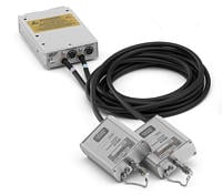
The 80E02 is a dual-channel, 20 GHz sampling modules and provides an acquisition rise time of 28. Optional 2 meter extender cable is available.
When used with Tektronix 80SJNB Jitter, Noise, & BER software, these modules enable separation of both jitter and noise into their components, understand precise causes of eye closure, and obtain highly accurate extrapolation of BER and 3-D eye contour. When used with 82A04 phase reference module, timebase accuracy can be improved down to 200 fsRMS jitter, which together with the 300 μV noise floor and 14 bits of resolution ensures the highest signal fidelity for the measured signals.
Characteristics
|
|
Application Type |
Channels |
Input Impedance |
Channel Input Connector |
Bandwidth*1 |
|---|---|---|---|---|---|
|
80E02 |
Low-level signals |
2 |
50 ±0.5 Ω |
3.5 mm female |
12.5 GHz*1 |
*1 Calculated from 0.35 bandwidth rise time product
|
|
Rise Time (10% to 90%) |
Dynamic Range |
Offset Range |
Maximum Operating Voltage |
Maximum Non-Destruct Voltage, DC+ACP-P |
Vertical Number of Digitized Bits |
|---|---|---|---|---|---|---|
|
80E02 |
≤28 ps |
1.0 Vp-p |
±1.6 V |
±1.6 V |
3.0 V |
14 bits full scale |
|
|
Vertical Sensitivity Range |
DC Vertical Voltage Accuracy, single point, within ±2 °C of compensated temperature |
Typical Step Response Aberrations*2 |
RMS Noise*2 |
|
|---|---|---|---|---|---|
|
(before step transition) |
(following step transition) |
||||
|
80E02 |
10 mV to 1.0 V full scale |
± [2 mV + 0.007 (Offset) + 0.02 (Vertical Value - Offset)] |
±3% or less over the zone 10 ns to 20 ps; |
+10%, –5% or less for the first 300 ps; ±3% or less over the zone 300 ps to 5 ns; ±1% or less over the zone 5 ns to 100 ns; ±0.5% after 100 ns |
1.8 mV, ≤2.3 mV (maximum) |
*2 Values shown are warranted unless printed in an italic typeface which represents a non-warranted characteristic value that the instrument will typically perform to
Physical Characteristics
|
|
Dimensions (mm/in.) |
Weight (kg/lbs.) |
||
|---|---|---|---|---|
|
|
Width |
Height |
Depth |
Net |
|
80E02 |
79/3.1 |
25/1.0 |
135/5.3 |
0.4/0.87 |


