Introduction
A technology change has taken place in digital communications in recent years with the introduction of high speed differential signaling. Differential signaling was once a niche application usually associated with long distance external interfaces, but is now being applied in almost all mainstream computer interfaces.Serial ATA is targeted to become the dominant data storage interface; FB-DIMM is targeted to become the dominant memory interface; and PCI Express is targeted to become the dominant I/O communication interface on computer processor boards. All three of these new computer interface standards use point-to-point, multi-gigabit, serial data communication with differential signaling at the physical layer.
It is natural with the migration towards differential signaling that high-speed measurement probe technology has also migrated from single ended ground referenced active probes to differential active probes.Differential probes are not only generally easier to use in measuring differential signals, but also provide significantly improved measurement performance.It is not surprising, therefore that many of the highest performance probes now being introduced are differential rather than single-ended designs.
Although differential signals are becoming much more common, there is still a strong need to make singleended measurements. Since a differential signal is actually composed of two complementary, single-ended signals, there is also a need to make single-ended measurements on differential signals. Single-ended measurements on differential signals are needed to measure the signal common mode response and to also check for asymmetry in the signal pairs that, if excessive, can lead to problems in the differential response.Fortunately differential probes have the flexibility to make single-ended measurements. In fact, in many ways differential probes are superior to single-ended probes for making single-ended measurements. This paper will examine the use of differential probes in making single-ended measurements on differential signals and consider measurement issues that arise when making such measurements.
Oscilloscope Probe Design
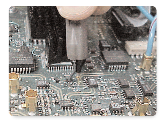
An oscilloscope probe is a tool for extending the measurement performance of an oscilloscope from its front panel input connector to the circuit to be measured. A high performance oscilloscope probe provides several important functions that help to preserve measurement fidelity as part of this interconnect mechanism:
- – Signal transmission to the host oscilloscope with high bandwidth and linear response
- – Signal buffering at the probe tip for reduced circuit loading
- – Signal shielding along the probe transmission path for reduced external noise injection
- – Signal interconnect flexibility for ease of use and reliable attachment to the probed circuit
Because of the probe requirements for high bandwidth and low noise performance, all oscilloscope probe designs are based on the use of coaxial cables for signal transfer. Coaxial cable, because of its uniform transmission line structure, provides much higher frequency response performance than a simple wire interconnect. In addition, coaxial cable has an inherent electrical shielding that helps to reduce the injection of noise from external sources. A typical probe design includes a probe tip for circuit attachment, a coaxial transmission line for signal transfer, and a probe control interface for connection to the oscilloscope front panel connector.
Oscilloscope probe designs have evolved over the years to meet increasing measurement performance demands.Early probe designs used primarily passive circuit technology to interface to high impedance oscilloscope channel inputs. Since high impedance passive probes are limited to about 500 MHz bandwidth and low impedance passive probes may have unacceptable DC signal loading, passive probe designs have significant limitations for today's high-speed applications and thus will not be examined in this paper (more information on passive probes can be found in the primer "ABCs of Probes" on www.tek.com). The focus of this paper is active probe design and measurement, in particular, the migration from single-ended to differential probe architectures.
An active probe uses a buffer amplifier in the probe tip to reduce probe loading and to drive the 50 ohm probe coaxial transmission line. The probe coaxial transmission line is terminated behind the oscilloscope front panel connector at the 50 ohm input of the oscilloscope vertical channel pre-amp. A single-ended active probe is designed for making ground-referenced signal measurements and has two inputs at the probe tip, a signal input and a ground connection. A picture of the Tektronix model P7240, a 4 GHz single-ended active probe, is shown in Figure 1 with a flexible, variablespacing ground lead used to make connection to the circuit ground. The P7240 probe has input connection sockets for both the signal pin and ground contact. The use of sockets allows for easy replacement of a worn signal input pin and flexibility in the choice of a ground contact. Unfortunately the parasitics inherent in a conventional socket structure limit the usability of sockets in the highest bandwidth probe designs. The type of ground connection employed on a single-ended probe is also a critical factor in making measurements with good signal fidelity, as will be examined in detail shortly.
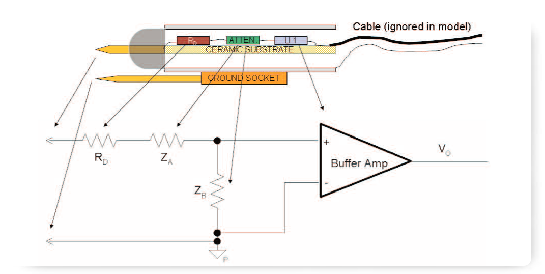
A simplified model of a traditional single-ended active probe is shown in Figure 2. The model shows the key elements of a typical single-ended active probe:
- – An input signal pin to contact the circuit to be measured
- – A ground contact which is connected internally to the probe attenuator, buffer amp, and cable shield
- – A probe input damping resistor to increase the probe input impedance at high frequencies and reduce probe resonant circuit problems
- – A compensated attenuator with high DC input resistance, wide bandwidth performance, and Offset voltage control for dynamic range extension
- – A probe buffer amplifier with low input capacitance, wide bandwidth performance, and high current output to drive the probe cable transmission line
- – A probe coaxial cable that is usually at least a meter long for convenient signal access and high performance signal transmission to the host oscilloscope
Although not shown in the simplified model, the probe cable transmission line also includes a set of additional wires to supply power to the probe buffer amplifier and possibly additional control signals, such as Offset voltage. (Some additional information on probe modeling can be found in the Technical Brief “TekConnect Probes: Signal Fidelity and Modeling" on www.tek.com.)
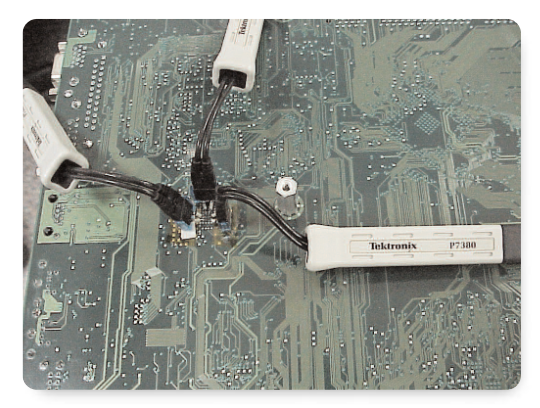
A differential active probe also contains a buffer amplifier but, unlike the single-ended active probe, its input attenuator and amplifier input stage have a balanced differential structure. A differential probe buffer amplifier essentially performs a differential to single-ended conversion on the input signal. For high speed serial data signals using differential signaling, this probe conversion allows measurement of a differential signal pair on a single oscilloscope vertical channel. A differential probe effectively acts like an ideal differential signal receiver and tries to show what a differential receiver input would see. A picture of the Tektronix model P7380, an 8 GHz differential probe is shown in Figure 3 with solder-down Tip-Clip™ Assemblies used to connect probes to differential data signal pairs.
A variety of different tip-clip adapters are available for the P7380 probe for solder-down or variable-spacing handheld and fixtured applications.
A simplified model of a differential active probe is shown in Figure 4. The matching of the balanced, differential input structure of a differential probe is critical to its differential measurement performance, particularly at high frequencies where parasitic elements can significantly affect the response. Since one of the key measurement advantages of a differential probe is its rejection of common mode noise, especially at high frequencies, matching of the input signal paths and the buffer amplifier input stage in a differential probe is a crucial design task for high CMRR performance. While both the single-ended probe and differential probe models have a similar looking amplifier symbol, a differential probe buffer amplifier is optimized for high CMRR.
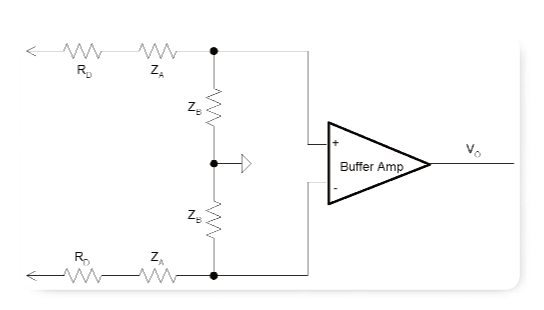
Comparing the single-ended and differential probe models in Figure 2 and Figure 4, it can be seen that the single-ended probe is fundamentally an asymmetric structure. The input impedance of a single-ended probe signal input is usually quite high at DC and decreases with frequency due to the capacitive elements in the probe input attenuator. The input impedance of a single-ended probe ground contact, on the other hand, is very low at DC (as anyone who has shorted out a circuit board power supply with a probe ground lead will agree) but increases significantly at high frequencies due to the inductive nature of the probe ground lead. The input impedance of differential probe inputs is by contrast very symmetric and each input acts like the singleended probe input already described. A separate ground connection for a differential probe is not usually needed or desirable. The lack of a ground contact on a differential probe is an advantage in making high fidelity measurements as will be shown shortly.
Both single-ended and differential probes require a twopoint contact interconnect to the circuit to be measured. Probe contacts need variable spacing capability for flexibility in connecting to different circuits with undefined contact spacing. Although flexibility in contact spacing is a useful feature, full bandwidth performance will generally limit the variable spacing range to a couple hundred mils for today's high performance probes. Wider contact spacing is usually possible, but only with reduced probe performance. The signal input contact on a single-ended probe is usually a short, fixed pin in order to optimize probe loading and measurement performance. Variable spacing of the probe contacts on a single-ended probe is usually done with a flexible or variable length ground lead. For a differential probe, which requires balanced signal inputs, variable spacing contact implementations depend on the interconnect type. In the case of a solder-down interconnect, simply adjusting the spacing of the probe input damping resistor leads or probe tip-clip input wire leads varies contact spacing. In the case of a handheld or fixtured interconnect, a special variable-spacing adapter is usually available with input pins whose spacing can be adjusted manually over a limited range.
The signal fidelity of a probe measurement can also be affected by the quality of the probe contact to the circuit to be measured. In the case of a solder-down interconnect, the probe contact is usually excellent unless poor solder technique results in a cold solder joint. In the case of a handheld or fixtured interconnect, it is important that both probe contact pins make solid connection to the circuit nodes. Contacting only one of the two input pins may appear to give a valid signal, but measurement fidelity is actually compromised, often very significantly. The best probe interconnect designs provide mechanical compliance of the probe input pins to balance the applied forces between the two input pins so that both pins tend to contact the circuit connections reliably. In the case of a single-ended probe, mechanical compliance is usually provided by the use of a spring-loaded or springy ground lead connection. In the case of differential probes, mechanical compliance in some new probe designs is achieved with the use of elastomeric pads in the handheld or fixtured adapters.
A single-ended oscilloscope probe has a ground connection on the probe tip which is designed for attachment to a ground reference point on the circuit to be measured. The voltage measured by a single-ended probe is the voltage difference between the signal connection and this ground reference connection. As already noted this is inherently an asymmetric measurement configuration, which can lead to some difficult challenges for measurement fidelity. Since the ground reference connection is the source of a number of potential measurement problems, it is important to understand the nature of ground as used in electronic circuit applications.
Signal and Probe Grounding
Historically a ground connection was just what it sounds like – a conductive connection to the soil of the earth. Developers of the telegraph, the first serious electrical communication system, discovered that soil was generally conductive enough to be used as the return current path for binary telegraph signals. Although the earth ground return path proved too noisy for analog voice communication in the telephone system that followed, direct earth grounding is still used today in electrical power distribution systems. In electrical power distribution earth ground is used as a safety connection to protect people and equipment from excessive voltage levels by sinking electrical fault-condition currents.
In electronic equipment the concept of ground has been incorporated as a common reference voltage for all internal signals. This internal signal ground is also typically connected through a low impedance path to both the equipment chassis and the power system safety ground. An ideal signal ground is a perfect zero volt reference which can be used to sink or source signal return currents with no change in voltage level. This zero resistance, zero inductance ground reference does not exist in reality, although it shows up regularly in schematic diagrams. A perfect ground is a conceptual simplification that has significant limitations, particularly with today's high-speed circuit designs. If the effects that result from non-ideal ground impedance, particularly the inductive component, are not well understood, serious circuit design problems can occur and signal measurement errors can easily be made.
Although ground is shown on most circuit diagrams as simply a common schematic symbol, the actual physical layout of the ground structure in an electronic circuit design is highly important for both noise control within the circuit and noise suppression outside the circuit. This is particularly true with today's high-speed circuit designs where many signal connections must be handled as transmission lines and where crosstalk between signals has become a significant design constraint.
The most common ground structure in high-speed designs is a full circuit board ground plane that provides both a low resistance and, probably more importantly, a low inductance ground reference connection.
Although not explicitly shown on most schematic diagrams, one of the other key features of a signal ground is to provide a path for signal return current. One of the primary reasons that a ground plane is used in high-speed designs is to provide a controlled signal return current path, which helps to isolate signals from each other. An inner layer ground plane is commonly used to establish a microstrip transmission line structure for signal traces on the circuit board surface. Because of the high mutual inductance between the signal trace and its ground plane, the signal return current flows primarily in the low inductance channel directly under the signal trace. The physical topology of the plane layer in this microstrip transmission line is the key factor in establishing this closely coupled return current path, since a power supply plane layer can provide the same low inductance return current path as a ground plane. The power plane in this case acts like an AC ground structure and generally requires a good array of bypass capacitors to allow return current to flow between power plane and ground plane layers where necessary.
The use of a multi-layer circuit board with full ground and power supply planes and a good distribution of bypass capacitors also meets the need in high-speed designs for a low impedance power supply. Without a low impedance power supply, there can be significant ground potential differences across the ground plane due to the effect of switching currents that flow through the ground plane layer. The use of bypass capacitors distributed across the circuit board tends to localize the effect of switching currents and helps to reduce the size of these voltage transients. Non-zero impedance in the power supply distribution results in not only potential differences across both the power and ground planes, but also generates common mode noise voltages relative to chassis ground, which may result in radiated noise from wires or cables connected to the ground plane.
The use of a ground plane layer helps not only to control the path of signal return currents but also to suppress the injection of noise due to electromagnetic field coupling effects. Because of the relatively low impedance level of most high-speed signals, noise coupling effects in high-speed designs are primarily inductive rather than capacitive. Magnetic fields generated by high-speed signal current changes in one signal loop can affect other nearby signal loops through mutual inductive coupling. The high density of signals in today's high performance circuit designs tends to exacerbate this crosstalk problem between signals. Since the degree of inductive coupling is dependent on the exposed loop area, the use of a ground plane spaced close to the signal traces reduces the loop area, which reduces the magnitude of noise coupling.
Oscilloscope probe voltage measurements are always made between two circuit nodes. For a single-ended voltage probe, which has a signal input and a ground connection, one of those circuit nodes is always ground. Because of an internal ground connection in the probe, it might seem possible to make a single-ended probe measurement by connecting only the probe signal input to the circuit to be measured. It is in fact the case that a signal input-only probe connection will display a signal waveform, particularly for a low input capacitance active probe. Unfortunately the ground loop formed by a signal input-only probe connection is very large and includes the path of the probe cable ground back to the oscilloscope, the path through the oscilloscope chassis to the oscilloscope power supply safety ground, the path through the AC power distribution network to the measured circuit power supply, and finally the path to the local circuit ground. This large loop area exposes the probe measurement to the potential for significant noise injection into the measured signal. Because of possible noise injection, it should be expected that this signal input-only probe connection would be highly sensitive to
probe position and movement. It is also likely that high frequency components of the signal will find a local return current path through parasitic capacitive coupling between the probe tip ground shield and the circuit ground. Without a low inductance probe ground lead connection, a signal input-only probe connection is also affected by a probe input resonance due to the probe tip capacitance and the relatively large parasitic inductance in the long probe cable shield and ground path.
Even when a probe ground lead is attached to the circuit to be measured, there are still some measurement fidelity issues that need to be considered:
- – The measured circuit signal may experience some perturbation due to the loading of the probe signal input connection.
- – The probe ground connection may cause some noise injection into the measured probe signal due to common mode current flow in the probe ground lead and shield from ground potential differences between the measured circuit and the attached oscilloscope.
- – The probe measurement ground loop may pick up inductive noise coupled from other signal loops near the measurement point.
- – With a probe ground lead attached to the local circuit ground a probe input resonant circuit still exists, but at a much higher frequency than the signal input-only probe connection, due to the lower probe ground path inductance of a short probe ground lead. Ideally this probe input resonance frequency is above the bandwidth of the probe where its effect on measurement fidelity is minimized.
Almost all of the above probe problems can be helped significantly by keeping the probe lead ground connection as short as possible. The ideal probe ground connection would be a coaxial connection, although that is generally not practical for normal use.
Considering the above list of possible problems, it might seem surprising that single-ended probe measurements with good signal fidelity can even be made on a highspeed circuit. How is it possible, for example, to measure and compare two signals that are widely separated on a circuit board with two single-ended probes? Since the ground potential is very likely different between the two widely separated signals, where should the ground leads of the two probes be placed for best signal fidelity? The answer is to place each probe ground lead at a ground node close to the individual circuit node to be measured with as short a probe ground lead length as possible. Each probe is able to use the local signal ground reference even when there is a significant potential difference between the probe ground leads. This is possible primarily because of the noise rejection action of the probe tip and the probe cable assembly. The probe cable assembly is a coaxial cable, which is shielded against capacitive-coupled noise signals, but more importantly, rejects common mode signals above the audio frequency range, both conducted and inductivecoupled. In a coaxial cable the signal propagates down the center conductor and the signal return current propagates back down the inner surface of the cable shield. Because of the tight coupling between the center conductor and the inner surface of the shield, a coaxial cable acts like a common mode transformer (see Henry Ott text “Noise Reduction Techniques in Electronic Equipment”*1). A common mode transformer is DC coupled and passes normal mode signals without attenuation but rejects common mode signals above the shield cutoff frequency, which is in the audio band for most coaxial cables. The probe tip structure is also shielded and is effectively an extension of the probe cable coaxial path. This common mode signal filtering action by the probe enables the probe to make measurements with good signal fidelity even in a relatively noisy environment. The weak link in this common mode noise filtering is the probe ground lead. Because the probe ground lead is not an extension of the probe coaxial structure, common mode noise current flowing on the probe ground lead is not rejected by the common mode transformer action, but appears as noise coupled into the measured signal. The probe ground lead length should thus be kept as short as possible to minimize ground lead inductance noise coupling.
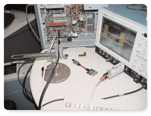
A differential active probe generally has balanced, high impedance signal inputs and no accessible ground contact. Some differential probes may have a ground connection socket for use with battery-powered measurement applications where a ground reference is needed, but in general high performance differential probes do not have an accessible ground contact. A differential probe input attenuator is ground referenced to its host oscilloscope, but there is usually no need to connect the internal probe ground to the measured circuit ground, in fact making such a connection may introduce some of the grounding problems seen with single-ended probes. The lack of a ground contact and the balanced signal inputs on a differential active probe provide the following advantages when compared to a single-ended probe:
- – No perturbation of the measured circuit ground reference by the introduction of a probe ground connection
- – No injection of noise signals into the measured signal path by the introduction of a probe ground loop
- – Reduction of common mode noise signals due to the balanced probe input structure and the high CMRR of the probe
- – No problem with circuit signal or power supply shorting caused by inadvertent connection to the probe ground contact
A new style of differential active probe that has recently been introduced is an SMA-input probe. The Tektronix model P7380SMA, an 8 GHz SMA-input probe, is shown in Figure 5 connected to a high-speed serial data signal breakout board with an SMA connector interface. SMA-input probes are designed for compliance testing of high-speed serial data signal paths where the probe both terminates and measures the signal (Additional information on serial data compliance testing can be found in the application note “The Basics of Serial Data Compliance and Validation Measurements" on www.tek.com.). Both inputs on an SMA-input probe have a 50 ohm input impedance rather than a high input impedance in order to provide a clean signal termination for most new serial data standard signals. The P7380SMA probe also has an adjustable termination voltage connected to its input termination resistors in order to reduce signal DC bias loading problems without requiring AC coupling. The differential signal connection to the measured circuit is made with a loss-compensated, delay-matched cable assembly. This cable assembly, of course, introduces a ground contact to the measured circuit through the SMA connector ground. The coaxial probe contact, however, should not experience the same ground noise coupling problems noted for typical single-ended probe grounds because of the completely shielded coaxial nature of the SMA connector ground contact.
Although a differential probe is the ideal tool for making differential measurements, other measurement approaches have also been used. Two single-ended probes, for example, can be used to make a differential measurement with the waveform math feature available on most high performance oscilloscopes used to calculate the signal difference. This pseudo-differential measurement, however, has some signal fidelity problems compared to a differential probe measurement. These problems result from both the single-ended probe grounding issues and from reduced CMRR due to high frequency matching difficulties between two separate probes and two separate oscilloscope channels. Since the measured signal delays are not well matched in the probes or scope channels, the pseudo-differential measurement method also requires an oscilloscope deskew operation before accurate pseudo-differential measurements can be made. A differential probe, by comparison, has no real disadvantages in making single-ended measurements. As will be shown in the following section, a differential probe is an excellent measurement tool for making single-ended measurements.
Single-ended Measurement Performance with Differential Probes
A differential probe can be used to make single-ended measurements by using its negative polarity input as a ground reference contact. Although a differential probe can be used as a single-ended probe, it is worth examining in more detail how well a differential probe performs in making single-ended measurements. The comparison between single-ended probe and differential probe grounding has already described some of the noise performance advantages of using a differential probe for making single-ended measurements. A more quantitative analysis of the noise rejection performance advantage of a differential probe will now be presented along with a discussion of several other single-ended measurement performance issues that should be considered when using differential probes.
Perhaps the first question that should be asked about the single-ended measurement performance of a differential probe is how accurate is the probe response. A well-designed differential probe will exhibit excellent performance matching between its single-ended response and its differential response. The gain and frequency response of both input polarities of a welldesigned differential probe must match closely in order to guarantee good differential response. Because of the greater ease of making single-ended frequency response validation measurements, differential probe performance is often validated by making single-ended performance measurements of both input signal polarities. With a well-matched probe input design, validation of single-ended signal response ensures accurate differential signal performance.
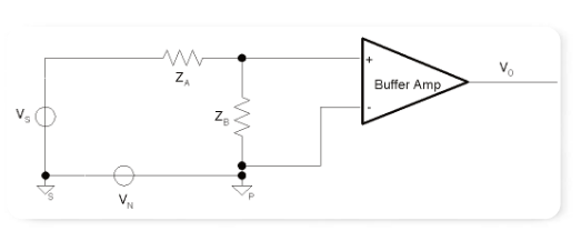
There are several advantages to using a differential probe to make single-ended measurements that were detailed in the previous section on probe grounding. A simplified, but more quantitative, analysis of the rejection of ground noise by a differential probe input structure will now be presented. A simplified model of a single-ended active probe input is shown in Figure 6. This model ignores details like the effect of source impedance and probe input damping resistance so that the analysis can focus on the effect of the noise voltage between the probe and circuit grounds. The assumption is also made that the buffer amplifier has unity voltage gain.
Since the noise voltage between the probe and circuit grounds is effectively in series with the circuit source voltage, the output voltage from the buffer amplifier is
VO = (VS + VN) * [(ZB / (ZA + ZB)]
VO = VS * [(ZB / (ZA + ZB)] + VN * [(ZB / (ZA + ZB)]
The second term in this probe buffer amplifier output voltage expression represents the ground noise term, which has the same effective gain as the source voltage in this simple model. It can be seen that noise voltage between the probe buffer amplifier ground and the measured circuit ground will be picked up in the measured signal output from the probe.
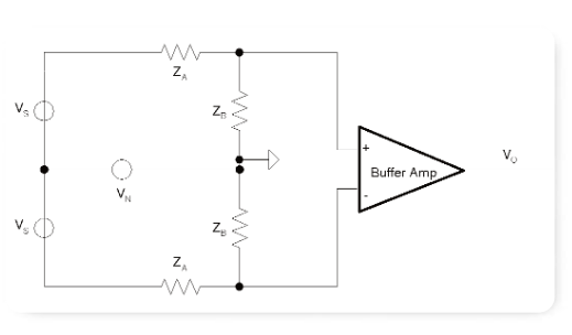
A simplified model of a differential active probe is shown for comparison in Figure 7. This differential probe model has the same simplifications as the previous single-ended probe model, but includes both a balanced source drive and a balanced probe input structure. The source common mode voltage is assumed to be zero volts in this simplified mode
Since the noise voltage between the probe and circuit grounds is effectively in series with both probe input paths, its effect is cancelled at the probe output by the differencing action of the probe input structure as shown below:
VP = (VDP + VN)* [(ZBP / (ZAP + ZBP)]
VN = (VDN + VN)* [(ZBN / (ZAN + ZBN)]
The resulting differential mode output voltage from the differential buffer amplifier with the common mode voltage is
VO = VP - VN = [(VDP + VN) - (VDN + VN)] * [(ZB / (ZA + ZB)]
Which reduces to the following expression with the ground noise term cancelled out
VO = (VDP - VDN) * [(ZB / (ZA + ZB)]
The ground noise term in this simplified analysis cancels out completely because the CMRR of these ideally matched probe input attenuators is infinite. In a realistic probe input structure there would be some probe input attenuator mismatch and it would typically become much worse with increasing frequency due to the effect of parasitic elements not shown in the simple model. If there were a tenth of one percent impedance mismatch between the attenuators of the differential probe inputs at DC, this would result in about a 60 dB CMRR. At a frequency of 1GHz the effect of parasitics in both the probe input attenuator and the probe buffer amplifier might reduce the probe CMRR to perhaps 40 dB for a well-designed differential probe, which represents about a one percent signal path mismatch. At the full probe bandwidth the probe CMRR might be expected to drop another order of magnitude to perhaps 20 dB or less
Because the degree of ground noise cancellation is dependent on the CMRR of the differential probe measurement structure, it is worth noting that signal source impedance mismatch can degrade the CMRR and thus the ground noise cancellation. This is particularly the case for single-ended signal measurements, which have an asymmetric source impedance because of the signal ground connection. For high-speed signals, which generally have a low source impedance to support a transmission line signal environment, the effect of source impedance mismatch is small at DC for a single-ended measurement. A 50 ohm source impedance mismatch for a single-ended signal measurement has only a minor effect on the DC CMRR of a probe with a 50 Kohm probe input impedance. As the signal frequency increases however, the probe input impedance begins to decrease and eventually this 50 ohm source impedance mismatch for a single-ended measurement can become quite significant. High frequency AC common mode voltage transients that may be largely rejected by the relatively high CMRR in a differential measurement may show a noticeable effect due to degraded CMRR in a single-ended measurement.
An active probe buffer amplifier is designed to accurately reproduce a signal present at its input by transmitting the measured signal at the probe tip to an oscilloscope channel input at the end of the probe cable. Accurate signal reproduction requires that the probe buffer amplifier be linear and have a well-controlled pulse response.Good pulse response results from a probe design with relatively constant gain over its frequency range, a smooth and moderate gain roll-off at it bandwidth limit, and compensation for known parasitic effects such as probe cable loss. A probe buffer amplifier however exhibits linear response only over a limited range. The linear operating range of an active probe buffer amplifier is limited by both the probe power supplies provided by the host oscilloscope and the amplifier architecture.
Several different voltage ranges are usually specified to define the input voltage range limits of an active probe. The widest voltage range specified is usually the non-destructive input voltage range, which indicates the absolute maximum voltage that can be applied to the probe tip without physical damage to the probe. The non-destructive input voltage range is usually a thermal damage or breakdown voltage limit and may include an allowable voltage application time limit. Although not always specified, short-duration high voltage events such as electrostatic discharge impulses can also permanently damage a probe input. This is particularly true of high frequency probe inputs that generally have physically small input components. It is always good practice to wear an antistatic wrist strap connected to the host oscilloscope chassis ground terminal when using high performance active probes.
The widest voltage range specified for useable probe operation is the input common mode voltage range or operating voltage window. The input common mode voltage range represents the allowable voltage window over which the more limited probe linear dynamic range can be swept, either with voltage offset for single-ended measurements or automatically due to probe CMRR for differential measurements. Since active differential probes automatically suppress common mode input voltage, violation of the common mode voltage limit must be verified by making single-ended voltage measurements. Attempting to measure signals beyond the operating voltage limit will usually result in non-linear response compression and eventual signal limiting.
The actual linear operating voltage range specified for an active probe is called the probe dynamic range.Because of the requirement for high speed, linear response, an active probe dynamic range is usually a fraction of the probe power supply range and is influenced most by the probe architectural design and the probe input attenuator attenuation factor. In fact a probe input attenuator is commonly used to extend the effective dynamic range of an active probe beyond the inherent dynamic range limit of the probe amplifier alone. Some probes even include a selectable attenuation factor to allow a tradeoff between probe dynamic range and noise floor.
The linear operating range of a high performance probe amplifier is limited by design in order to meet the signal risetime and bandwidth requirements and still stay within reasonable probe amplifier power dissipation limits. Because the internal probe amplifier circuit node voltages must be charged and discharged at very fast rates, limiting these voltage swings helps high frequency performance but reduces the linear operating range.Similarly limiting the current available to charge and discharge the internal probe amplifier circuit nodes helps power dissipation but also reduces the probe frequency response. Because of the many design tradeoffs required to meet overall probe performance requirements, probe dynamic range often ends up as a compromise that meets most but not all application requirements.High performance probes are generally designed for high performance applications and not for more general purpose use.
For single-ended measurements with a significant DC voltage component, it is possible to extend the effective probe dynamic range by using the probe voltage offset control. Many high-speed serial data signals have a DC bias in order to allow single power supply operation, but typically have a significantly smaller digital signal swing for high-speed switching capability. As an example, a DVI/HDMI differential signal, which is used for high speed I/O between a computer and a video display monitor, uses complementary CML logic drivers to drive 50 ohm transmission lines. The CML logic drivers are terminated with 50 ohm resistors to the CML receiver Vcc power supply. If Vcc is +3.3V, a typical single-ended CML signal might swing between +3.3V and +2.7V. For a DC-balanced signal this results in a +3.0V common mode voltage and a 600mVpp switching signal. For a probe like the P7380 with 5X and 25X attenuation settings, either attenuation setting has sufficient dynamic range to measure a 600mVpp signal, but the 5X attenuator setting would generally be preferred for its lower noise floor. Both attenuator settings require the use of Offset voltage control to null out the +3.0V DC bias and move the digital signal swing into the probe dynamic range window when making this single-ended measurement.
Using Differential Probes to Measure Differential Signal Asymmetry
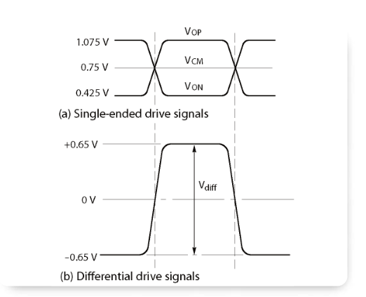
A differential signal is composed of two complementary driven ground referenced signals. The two complementary signals ideally are matched, but inverted in signal polarity.In order to generate a differential signal using a single power supply voltage, a differential signal pair is typically sourced with a common mode bias. This bias voltage shifts the level of the complementary signal swing within the operating voltage range of the differential receiver.A differential receiver or measurement probe effectively removes this transmitted common mode bias due to its high DC CMRR. An example of a transmitted differential signal pair with common mode bias and the resulting differential mode signal as seen by a differential receiver or probe is shown in Figure 8. (More information on differential signaling can be found in the primer "HighSpeed Differential Signaling and Measurements" on www.tek.com).
To fully characterize a differential signal requires measurements of three separate probe placements:
- - A differential measurement between the two complementary signals (DIFF)
- - A single-ended measurement between the positive polarity signal and ground (SE+)
- - A single-ended measurement between the negative polarity signal and ground (SE-)
These three measurements are made sequentially in the examples that follow and the measured waveforms are stored in the oscilloscope on a common triggered display to show amplitude and timing relationships.
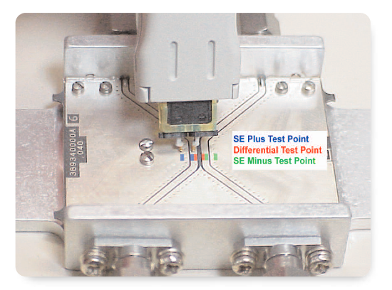
The location of probe pin connections on the differential probe test fixture used in the following examples is shown in Figure 9. The probe test fixture board has differential coplanar waveguide transmission lines.Although it is possible to make these three measurements by soldering down three separate tip-clips, the loading effect of the unconnected tip-clips will slightly affect the signal measurement, particularly for high-speed signals. The best measurement fidelity is obtained by probing the different probe test adapter trace locations with a variable spacing tip-clip, moving the tip-clip pins in turn between the three measurement locations.
One of the primary reasons for measuring the singleended response of a differential signal is to identify signal specification violations or signal asymmetry that might contribute to differential signal quality problems.A common tool for characterizing high-speed serial data signal quality is an eye pattern display. An eye pattern display is an accumulation of signal transitions overlaid on top of each other in a single clock period window.An eye pattern display can be used to examine both amplitude and timing problems relative to an allowable signal template, sometimes called an eye pattern mask.If a differential measurement eye pattern shows either amplitude or timing irregularities, then single-ended measurements can be made to try to identify whether the source of the problem is one polarity or the other or a problem common to both. An eye pattern display is used in one of the examples that follow using a clock trigger provided by the signal source.
Although serial data signal specification violations can usually be identified from careful single-ended signal measurements, asymmetry between the supposedly matched differential signal pairs can sometimes be more difficult to categorize. Asymmetry between the signal pairs that form a differential signal can effectively convert some of the differential signal energy to common mode energy and similarly some of the common mode energy, which is not usually considered part of the differential signal, to differential mode noise. These mixed-mode conversion factors and their actual contribution to the resulting differential signal may not be easy to quantify, particularly since the common mode components of the signal are rejected to some degree depending on the receiver CMRR, which can vary significantly with frequency. A differential probe response is designed to model a high quality differential receiver, but is probably not an exact representation of an in-circuit receiver input. It is generally best for the single-ended signals in a differential pair to be designed as symmetrically as possible to minimize these asymmetry problems.
In the remainder of this paper several examples of differential signal pair asymmetry will be presented to show the effect of different types of asymmetry on differential signal response. Although the asymmetry examples shown will be more extreme than might be expected in a well designed serial data layout and communication channel, it will hopefully serve to show how important single-ended measurements can be in debugging differential signal problems. It will hopefully also show that differential probes are an excellent tool for making both differential and single-ended measurements.
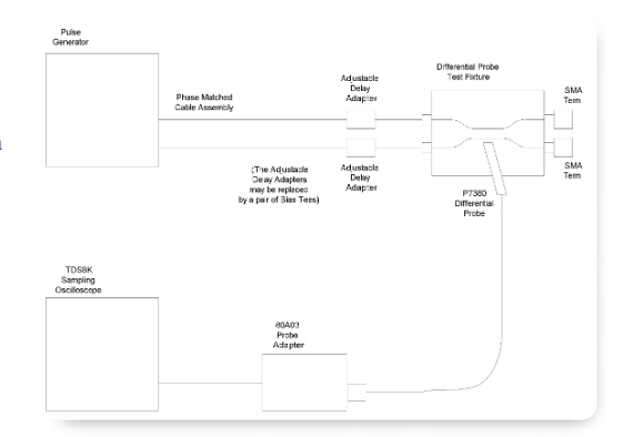
The equipment setup for these asymmetric signal examples includes the following signal source and common measurement tools:
- - Advantest D3186 Pulse Generator as a differential signal generator with amplitude and timing control
- - A pair of SMA adjustable delay adapters (Tektronix model 015-0708-00)
- - A pair of bias tees (PSPL model 5545-107)
- - Low loss, phase matched cable assembly (Tektronix model 174-4944-00)
- - Differential Probe Test Fixture
- - P7380 8GHz differential active probe with a variable-spacing tip-clip and handheld adapter
- - TDS8200 sampling oscilloscope with an 80A03 TekConnect Probe Adapter and a 12GHz 80E02 sampling module
The general equipment configuration is shown in Figure 10.
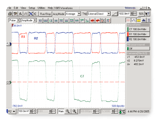
As a reference for the examples of asymmetry that follow, a measurement was made without any significant asymmetry. The waveforms shown in Figure 11 are representative of those in the examples that follow, but without the injection of specific asymmetry:
- - Waveform R1 (red) is the single-ended signal with negative polarity (SE-)
- - Waveform R2 (blue) is the single-ended signal with positive polarity (SE+)
- - Waveform C7 (green) is the differential signal (DIFF)
It is evident from the waveforms in Figure 11 that the two single-ended signals have complementary drive and are quite well matched in both amplitude and time. The resulting differential waveform in Figure 11 shows very little distortion and has an amplitude that is very close to twice the peak-to-peak value of the single-ended signals as is expected.
Both amplitude and timing asymmetry between the pair of signals that form a differential pair can contribute to differential signal quality problems. The types of asymmetry that may be present in a differential signal pair include the following variations:
Amplitude:
- - Peak-to-peak voltage
- - Common mode voltage bias
- - Reflections
- - Crosstalk
- - Noise
Timing:
- - Risetime
- - Skew
- - Jitter
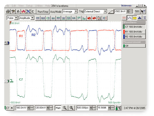
The first example in Figure 12 shows the effect of asymmetry between the signals of a differential pair caused by reflections in one of the signal paths that is not present in the other. Asymmetry due to signal reflections is generally the result of layout differences in the routing of a differential signal pair. Even when care is taken to closely match the routing paths and terminations of differential signal traces, it is not uncommon to have differences occur, particularly at high-density IC pin locations or connector interfaces. Even signal return current path differences can lead to reflection problems resulting for example from ground plane discontinuities in areas where vias are concentrated. Reflection asymmetry is simulated in the following example by terminating one of the signal paths at the end of the probe test adapter directly and the other through an SMA tee adapter. The SMA tee introduces an unterminated stub discontinuity that causes noticeable reflections with the 50ps signal risetime.
The reflection asymmetry example in Figure 12 show that the R2 (SE+) waveform has a very noticeable reflection and the R1 (SE-) waveform has almost none. This difference between the two single-ended waveforms results in the reflection appearing directly in the C7 (DIFF) waveform. If only a differential measurement were made, it would be obvious that there was a problem, but impossible to know which of the two single-ended signals might have a reflection problem or whether they both are contributing to the problem. Making singleended measurements then helps to identify the source of the reflection problem.
Although a single-ended probe could be used to measure the single-ended signal responses once a reflection problem had been observed on the differential signal using a differential probe, it is generally more convenient and probably more accurate to simply use the same differential probe to make these single-ended measurements.Using a differential probe to measure the single-ended signal response avoids the single-ended probe grounding problems already mentioned. Using the same probe to measure both the differential and single-ended signal response also avoids differences in probe loading and probe frequency response that are unavoidable when two different probes are used to make measurements.Although there will be some difference in probe response due to the source impedance difference between a differential and single-ended measurement,the overall differences are still minimized when a single probe is used for making both measurements. The most difficult problem with making single-ended measurements on a differential signal may be locating a good ground reference near the desired signal measurement point. It is often good practice to add extra ground vias around critical differential signals at expected measurement points. If the closest accessible ground connection to a signal to be measured is too far away from the signal, single-ended measurement performance may be significantly degraded.
The second example of signal asymmetry between the signals in a differential pair shows the effect of signal path skew. Signal skew usually results from a mismatch in the routing length of the signal traces in a differential pair connection path between a differential transmitter and receiver. Skew can also result when differential pair traces are not routed together through a common transmission medium; an example would be the routing of one trace on an outer circuit board layer as a microstrip and the other trace on an inner layer as a strip line.Since the signal propagation velocities differ in the different transmission media, trace length matching does not equal transmission delay matching. In this example of transmission delay asymmetry, skew is intentionally introduced with a pair of SMA adjustable delay adapters. These adjustable delay adapters use a sliding coaxial connection to mechanically adjust the signal delay between the SMA connectors of the adapter. As shown in Figure 13, the delay difference between the single-ended R1 and R2 signals is about 20 ps. Although 20 ps might not seem like a very large skew, it is about one third of the 60 ps signal risetime and does have an impact on the resulting differential signal delay.
The waveforms shown in Figure 13 present a timeexpanded view of a 2.5 Gbps signal eye pattern centered on the signal transitions. An eye pattern results from an accumulation of signal transitions from a serial data pattern (a PRBS-7 signal pattern in this example) triggered by a stable and synchronized data rate clock.
The spread of accumulated signal dots in the eye pattern display in Figure 13 is an indication of the jitter in the signal. The eye pattern display at this signal transition point shows clearly the signal rise and fall times, which appear to be quite similar in this example.Although the differential signal risetime appears to be well controlled in Figure 13, with no sign of degraded response that might indicate a differential pair mismatch problem, the single-ended measurements clearly show a timing mismatch problem. Only in an extreme case of skew where the skew exceeds the single-ended signal risetime will the differential response risetime show obvious aberrant behavior, such as a pedestal in the middle of the response risetime.
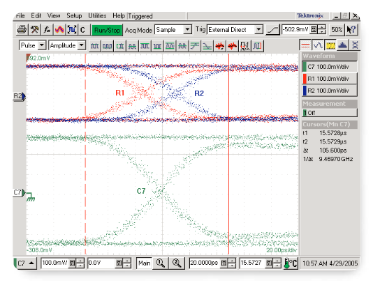
It can also be seen by carefully examining Figure 13 that the skew between the two single-ended signals results in an increase in the risetime of the differential signal.The skew between the two single-ended signals, R1 and R2, causes the signal transitions to extend over a longer time period in the differential signal response than would occur with no skew present. Since the R1 waveform (SE-) in Figure 13 begins its signal transitions about 20 ps before the R2 waveform (SE+) signal transitions, the resulting C7 waveform (DIFF) response begins its signal transitions at the beginning of the R1 transition. This initial differential response transition however occurs at about half the rate of transition as would occur with no skew, when both the R1 and R2 waveforms transition together in a complementary manner. After the 20 ps skew period from the beginning of the R1 transition, both the R1 and R2 waveforms transition together with opposite polarity, which results in an increase in the transition rate of the differential signal response to what would be expected without any skew. Finally, at the end of the R1 signal transition time period, the R2 signal transition continues for the duration of the 20 ps skew time, which also extends the duration of the differential response, but again at half the normal transition rate. It can be seen in Figure 13 that the center of the differential response transition occurs at the center of the skew period between the two single-ended signals. The skew between the two single-ended signals thus results in extending the differential response transition period.Although the risetime of the two single-ended signals is not slowed by the skew between the signals, the skew does slow the differential signal risetime. In this skew asymmetry example the 20 ps skew between the single-ended signals results in about a 10 ps increase in the differential signal risetime.
The final asymmetry example shows the effect of differences in the common mode bias between the single-ended signals in a differential pair. Although this may not be a common application problem, it does show the effect of single-ended signal voltage level differences on the differential response. The example shown in Figure 14 has a rather extreme bias voltage difference between the two single-ended signals, but it was intentionally made large to clearly show the effect.In a real world situation, voltage bias or amplitude asymmetry would probably be the result of driver or termination mismatch. In this simulated example the single-ended signal bias level is artificially controlled using a pair of SMA bias-tee adapters and a DC power supply to control the bias levels.
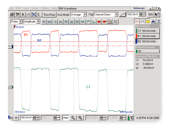
The different common mode voltage levels of the R1 (SE-) and R2 (SE+) waveforms are shown with straight and dashed horizontal cursors in the Figure 14 screen capture. Since both the R1 and R2 signals have an identical amplitude of 250mVpp, the 50mV bias voltage difference between the signals represents a 20% asymmetry, which is clearly visible. The effect of this DC bias voltage asymmetry on the C7 (DIFF) waveform is a DC level shift in the differential signal response. If the differential receiver driven by this level-shifted signal had its decision point set at zero volts, then the resulting receiver output would show a significant shift in duty cycle that would appear as increased jitter in an eye pattern display.
Conclusion
Traditionally single-ended probes have been used only for making single-ended measurements and differential probes have been used only for making differential measurements. With the increased availability of high performance differential probes this traditional paradigm is changing. There are a number of advantages in using differential probes for making single-ended measurements, especially for high-speed signal measurements.Since fully characterizing the quality of a differential signal requires making both differential and single-ended measurements of the differential signal pair, a differential probe is the recommended choice for making this full set of measurements.
Find more valuable resources at TEK.COM
Copyright © Tektronix. All rights reserved. Tektronix products are covered by U.S. and foreign patents, issued and pending. Information in this publication supersedes that in all previously published material. Specification and price change privileges reserved. TEKTRONIX and TEK are registered trademarks of Tektronix, Inc. All other trade names referenced are the service marks, trademarks or registered trademarks of their respective companies.
6/05 60W-18344-0

