THIS APPLICATION NOTE
- Gives a brief orientation on the physical layer and packet structures of I2C and SPI, with a goal of providing just enough detail to help with troubleshooting
- Explains how to set up decoding on an oscilloscope equipped with I2C and SPI decoding
- Explains how to interpret serial bus data on an oscilloscope equipped with I2C and SPI decoding
- Explains what triggering and searching options are available on an oscilloscope equipped with I2C and SPI
With the optional serial triggering and analysis capability, Tektronix oscilloscopes become powerful tools for embedded system designers working with I2C and SPI buses. In this application note the 5 Series MSO is used to demonstrate I2C and SPI serial bus decoding and triggering.
Tektronix 2, 4, 5 and 6 Series MSO oscilloscopes support I2C and SPI triggering and analysis. The operation of all of these instruments is practically identical to the 5 Series MSO used in this application note. See the Oscilloscope Selection Guide for more information.
Introduction
Most microcontroller-based designs use I2C or SPI or both, to communicate among controllers and between controllers and peripheral chips. Seeing what’s going on in an embedded system when a chip sends a particular I2C or SPI packet can be critical when you’re troubleshooting. Many chips that manage relatively slow parameters, such as temperature sensors, motor controls, human interfaces or power management, use these buses as their primary means of communications with the rest of the system. Other higher-speed chips, such as communications ICs, clocks and ADCs are often configured using these buses. For example, to troubleshoot a problem with a cooling fan after power-up, it can be helpful to look at the timing and structure of SPI commands being sent to the fan controller IC, as well as the drive signal to the fan and the power supply.
I2C and SPI buses are well-defined and relatively robust, but they can still be affected by noise, board layout, reset issues and subtle differences in implementations. These can sometimes result in bus errors and lock-ups. Oscilloscopes equipped with decoding capability allow you to see both bus data and the condition of bus signals simultaneously.
I2C
I2C, or "I squared C", stands for Inter-Integrated Circuit. It was originally developed by Philips in the early 1980s to provide a low-cost way of connecting controllers to peripheral chips. It has since evolved into a worldwide standard for communication between devices in embedded systems. This simple twowire design has found its way into a wide variety of chips like I/O, A/Ds, D/As, temperature sensors, microcontrollers and microprocessors from numerous leading chipmakers including: Analog Devices, Atmel, Infineon, Cypress, Intel, Maxim, NXP, Silicon Labs, ST Microelectronics, Texas Instruments, and others.
HOW IT WORKS
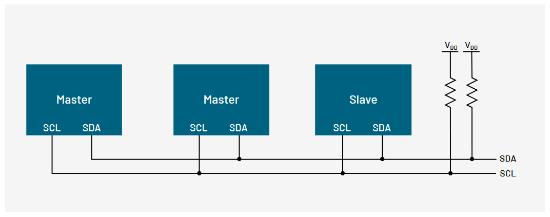
I2C’s physical two-wire interface is comprised of bi-directional serial clock (SCL) and data (SDA) lines. I2C supports multiple masters and slaves on the bus, but only one master may be active at a time. Any I2C device can be attached to the bus allowing any master device to exchange information with a slave device. Each device is recognized by a unique address. A device can operate as either a transmitter or a receiver, depending on its function. Three bit rates are supported: 100 kb/s (standard mode), 400 kb/s (fast mode), and 3.4 Mb/s (highspeed mode). The maximum number of devices is determined by a maximum capacitance of 400 pF or roughly 20-30 devices.
| START | ADDRESS | R/W | ACK | DATA0 | ACK0 | DATA1 | ACK1 | ... | DATAN | ACKN | STOP |
| 7 or 10 bits | 1 bit | 1 bit | 8 bits | 1 bit | 8 bits | 1 bit | 1 bit | 8 bits | 1 bit |
The I2C standard specifies the following format:
- Start - indicates the device is taking control of the bus and that a message will follow.
- Address - a 7- or 10-bit number representing the address of the device that will either be read from or written to. Initially, I2C only used 7-bit addresses, but evolved to allow 10-bit addressing as well. Three
- R/W Bit - one bit indicating if the data will be read from or written to the device.
- Ack - one bit from the slave device acknowledging the master’s actions. Usually each address and data byte has an acknowledge, but not always.
- Data - an integer number of bytes read from or written to the device.
- Stop - indicates the message is complete and the master has released the bus.
There are two ways to group I2C addresses for decoding: in 7-bits plus a read or write (R/W) bit scheme, and in 8-bits (a byte) where the R/W bit is included as part of the address. The 7-bit address scheme is the specified I2C Standard followed by firmware and software design engineers. But many other engineers use the 8-bit address scheme. Tektronix oscilloscopes can decode data in either scheme.
SETTING UP I2C BUS DECODING
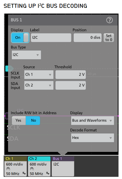
On Tektronix oscilloscopes, pressing the front panel Bus button enables you to define inputs to the scope as a bus. By simply defining which channels clock and data are on, along with the digital threshold levels used to determine logic ones and zeroes, you enable the oscilloscope to understand the protocol being transmitted across the bus.
INTERPRETING THE I2C BUS
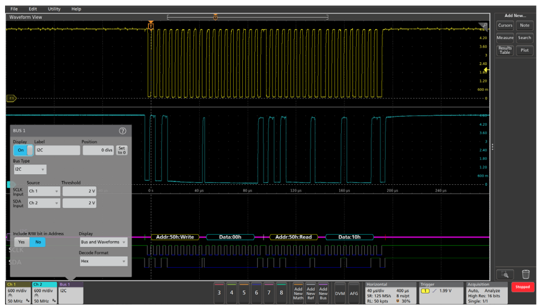
The time-correlated waveform and bus decode display is a familiar and useful format for many hardware engineers. The decoded bus waveform indicates the elements of an I2C message.
| I2C BUS ELEMENT | INDICATED BY |
| Starts Repeated starts occur when another start is shown without a previous Stop. |
 |
| Addresses [W] indicates a write and [R] indicates a read.Address values can be displayed in either hex or binary. |
 |
| Data Data values can be displayed in either hex or binary. |
 |
| Missing Acks |
 |
| Stops |
 |

For firmware engineers, the Results Table format may be more useful. This time-stamped display of bus activity can be easily compared to software listings, and allows easy calculation of the execution speed.
The Results Table also provides linkage back to the waveform displays. You can tap a line in the tabular display and the oscilloscope automatically zooms in on the corresponding bus signals and resulting decoded bus waveform, shown in the lower section of the screen.
TRIGGERING ON THE I2C BUS
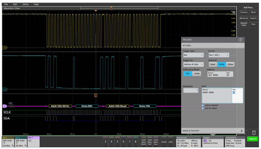
When debugging a system based on one or more serial buses, one of the key capabilities of the oscilloscope is isolating and capturing specific events with a bus trigger. When the bus trigger is correctly set up, the oscilloscope will capture all of the input signals and one specified bus event will be positioned at the trigger point. This example demonstrates triggering on address 0x50 and data 0x00.
| TRIGGER ON | DESCRIPTION |
| Start | Triggers when SDA goes low while SCL is high. |
| Repeated Start | Triggers when a start condition occurs without a previous stop condition. This is usually when a master sends multiple messages without releasing the bus. |
| Stop | Triggers when SDA goes high while SCL is high |
| Missing Ack | Slaves are often configured to transmit an acknowledge after each byte of address and data. The oscilloscope can trigger on cases where the slave does not generate the acknowledge bit. |
| Address | Triggers on a user specified address or any of the preprogrammed special addresses including General Call, Start Byte, HS-mode, EEPROM, or CBUS. Addressing can be either 7 or 10 bits and is entered in binary or hex. |
| Data | Triggers on several bytes of user specified data values entered in either binary or hex. |
| Address and Data | This allows you to enter both address and data values as well as read vs. write to capture the exact event of interest. |
SEARCHING THE I2C BUS
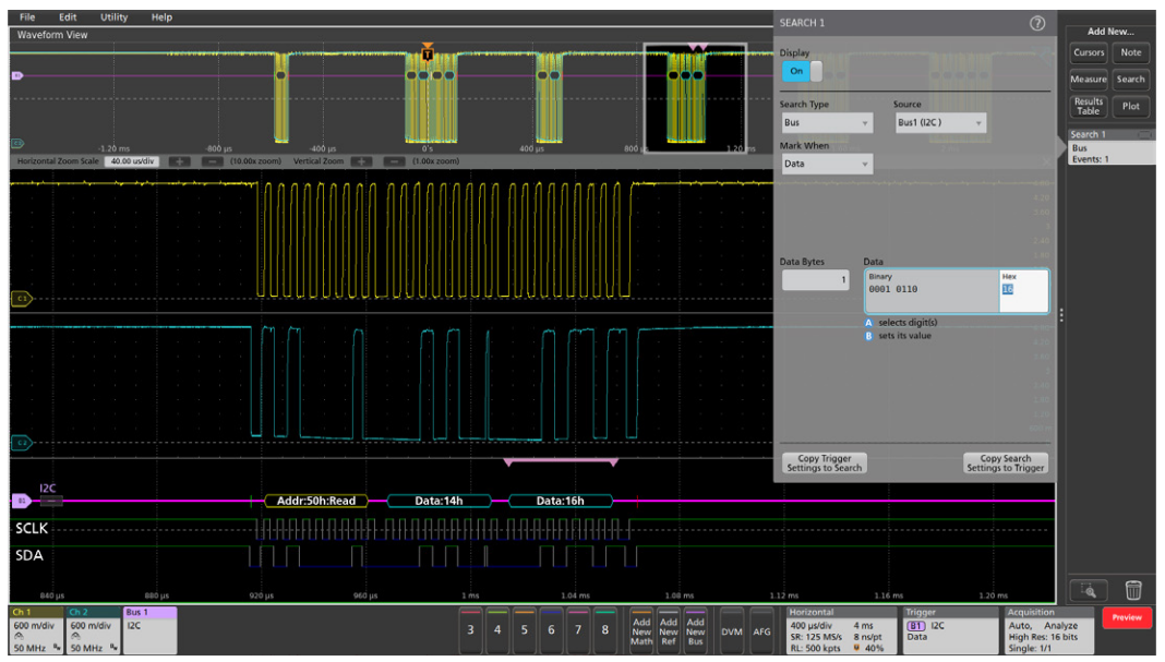
On a Tektronix oscilloscope you can use the automated Wave Inspector search to find all of the bus events that meet a search criteria and determine how many of them occurred. The setup is similar to the bus trigger setup, and allows the oscilloscope to find and mark all of the specified bus events. In this example, the automatic search is looking for the data value 0x16. This data value occurs only once in the acquired waveforms and the position of the serial data packet is shown with the pink bracket icon.
SPI
The Serial Peripheral Interface bus (SPI) was originally developed by Motorola in the late 1980s for their 68000 series micro-controllers. Due to the simplicity and popularity of the bus, many other manufacturers have adopted the standard over the years. It is now found in a broad array of components commonly used in embedded system design. SPI is primarily used between micro-controllers and their immediate peripheral devices. It’s commonly found in cell phones and other mobile devices to communicate data between the CPU, keyboard, display, and memory chips.
HOW IT WORKS
The SPI bus is a master/slave, 4-wire serial communications bus. The four signals are clock (SCLK), master output/slave input (MOSI), master input/slave output (MISO), and slave select (SS). Whenever two devices communicate, one is referred to as the "master" and the other as the “slave”. The master drives the serial clock. Data is simultaneously transmitted and received, making it a full-duplex protocol.
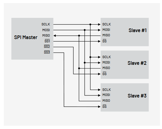
Rather than having unique addresses for each device on the bus, SPI uses the SS line to specify which device data is being transferred to or from. As such, each unique device on the bus needs its own SS signal from the master. If there are 3 slave devices, there are 3 SS signals from the master, one to each slave.

SPI can also be wired with the slave devices daisychained, each performing an operation in turn, and then sending the results back to the master (which can be used to verify the integrity of the data path).
In some cases, where communication from the slave back to the master is not required, the MISO signal may be left out altogether. In other cases there is only one master and one slave device and the SS signal is tied to ground. This is commonly referred to as 2-wire SPI.
When an SPI data transfer occurs, an 8-bit data word is shifted out on MOSI while a different 8-bit data word is being shifted in on MISO. This can be viewed as a 16-bit circular shift register. When a transfer occurs, this 16-bit shift register is shifted 8 positions, thus exchanging the 8-bit data between the master and slave devices. A pair of registers, clock polarity (CPOL) and clock phase (CPHA) determine the edges of the clock on which the data is driven. Each register has two possible states which allows for four possible combinations, all of which are incompatible with one another. So a master/slave pair must use the same parameter values to communicate. If multiple slaves are used in different configurations, the master has to reconfigure itself each time it needs to communicate with a different slave.
SETTING UP SPI BUS DECODING
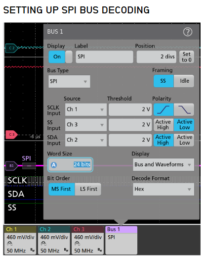
In this example, the SPI signals are being captured using passive probes on the analog channels (channel 1, channel 2 and channel 3) on the oscilloscope. Digital channels can also be used for bus decoding. Using the Bus configuration menu, you can define an SPI bus by specifying which channels are connected to the clock, data, and slave select signals, the thresholds, polarities, and word size.

INTERPRETING THE SPI BUS
By setting the display mode to Bus and Waveforms, the digital interpretation (comparison of the analog signal to the corresponding threshold voltage) of each of the input signals can be quickly verified. These digital signals (green is high and blue is low) are then interpreted according to the SPI protocol. When properly set up, the oscilloscope can display the decoded results.
| SPI BUS ELEMENT | INDICATED BY |
| Starts Repeated starts occur when another start is shown without a previous Stop. |
 |
| Data Data values can be displayed in either hex or binary. |
 |
| Stops |
 |
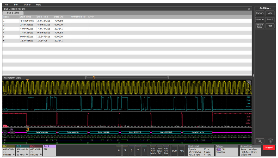
Consider an example system with daisy-chained SPI architecture. This subsystem controls a voltage-controlled oscillator (VCO) that provides the RF clock to the rest of the system. The VCO is initialized by the main CPU by writing six 24-bit words to the VCO. The signals appear to meet the electrical specifications for SPI, but the VCO is not generating the right frequency.
The Results Table view can be used to examine the VCO initialization. The oscilloscope can be set to trigger on the SPI Slave Select signal going active. When the system is powered up, the oscilloscope will capture and display the initialization sequence.
TRIGGERING ON THE SPI BUS
In the example above we used a simple SS Active trigger. The full SPI triggering capabilities in Tektronix oscilloscopes include the following types:
| TRIGGER ON | DESCRIPTION |
| SS Active | Triggers when the slave select line goes true for a slave device (3-wire mode). |
| Start of Frame | Triggers at the start of a frame when the clock idle time is used to define the frame timing (2-wire mode). |
| Data | Trigger on one or several bytes of user-specified data (MOSI or MISO). (The 4000/3000/2000 Series models can trigger on up to 16 bytes of MOSI and MISO data.) |
These triggers allow you to isolate and capture the particular bus traffic you’re interested in, while the decoding capability enables you to instantly see the content of every message transmitted over the bus in your acquisition.
SEARCHING ON THE SPI BUS
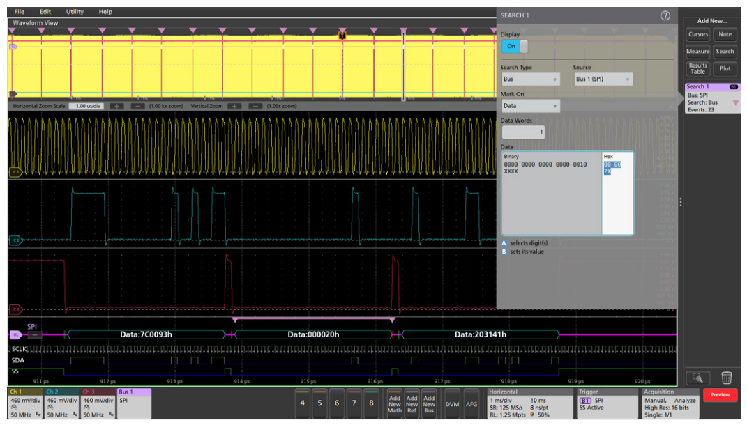
To find all of the bus events that meet a specific search criteria, the automated Wave Inspector search function can be used. The setup is similar to the bus trigger setup, and will find and mark all of the specified bus events. In this example, the automatic search is looking for the 24-bit data value 0x00002X. This data value occurs 23 times in the acquired waveforms. The front panel Navigation arrow buttons easily navigate between marked events. The position of one of the specified serial data packets is shown with the pink bracket icon near the bottom of the display.
Find more valuable resources at TEK.COM
Copyright © Tektronix. All rights reserved. Tektronix products are covered by U.S. and foreign patents, issued and pending. Information in this publication supersedes that in all previously published material. Specification and price change privileges reserved. TEKTRONIX and TEK are registered trademarks of Tektronix, Inc. All other trade names referenced are the service marks, trademarks or registered trademarks of their respective companies.
01/24 55W-61091-2

