Contactez-nous
Chat en direct avec un représentant Tek. Service disponible de 9 h à 17 h, CET jours ouvrables.
Appelez-nous au
Disponible de 9 h à 17 h CET jours ouvrables.
Télécharger
Télécharger des manuels, des fiches techniques, des logiciels, etc. :
Feedback
TekExpress MIPI D-PHY Test Application
DPO-MSO70000 Option DPHY12 and DPHY21, MSO6/6B 6-CMDPHY12 and 6-CMDPHY21
Plus d’informations
- Oscilloscope hautes performances DPO70000SX ATI
- Oscilloscopes au phosphore numérique et à signaux mixtes MSO/DPO70000DX
- Oscilloscope à signaux mixtes MSO 64B, 66B, et 68B
- Découvrez d'autres modèles Logiciel pour oscilloscopes, produits keithley, et RF
Lire en ligne :
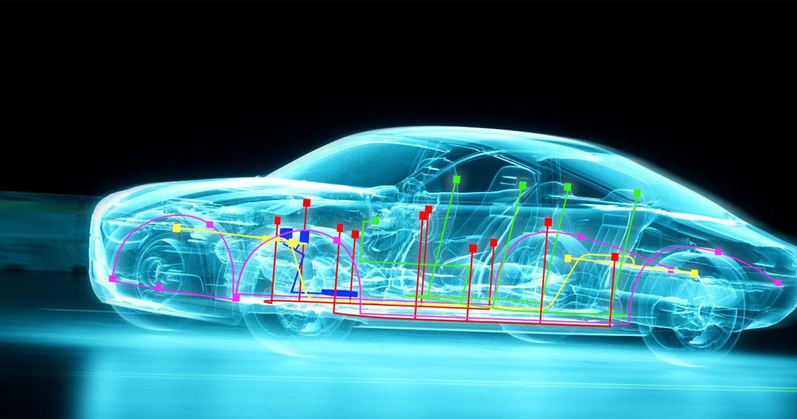
D-PHY or MIPI Display Phy is a standardized physical layer interface for connecting the Camera/Display to the Processor. This interface is predominantly used in mobile devices, infotainment systems and biometric sensors. This is a unidirectional bus with an explicit clock, up to 4 data lanes and consists of High Speed mode and Low Power mode. The High Speed mode is for fast data transfer and Low Power mode is for power saving to extend the battery life. The data flow in a display interface is from processor to the display device and from camera to the processor in the camera interface. The MIPI D-PHY specification testing is done based on the Compliance Test Specification (CTS) and requires a board with dynamic switching of termination between Low Power state and High Speed mode.
The Tektronix TekExpress® D-PHY application offers a complete physical layer test solution for transmitter conformance and characterization as defined in the MIPI D-PHY version 1.2 and version 2.1 specification. The automated test solution along with 70000 C/DX/SX or a 6 Series MSO instruments, provides an easy way to test, debug and characterize the electrical and timing measurements of D-PHY data links.
Key features (version 1.2)
Fully automated solution
- Performs D-PHY transmitter test with single-button click across High Speed (HS), Low Power (LP), Low Power-High Speed (LP-HS), and Ultra-Low Power State (ULPS) sequences in the D-PHY signal
- Select individual tests or groups of tests
- Improved test run time
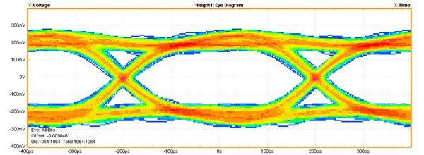
Eye Diagram Capability
- Displays the eye diagram of the High Speed signal with option DJA enabled on the scope for Test ID 1.5.4, Data to clock skew test and Test ID 1.5.7 HS-TX Data and Clock Eye Diagram
Image Snapshot
- Option of including the snapshot of the first reference region of analysis in the captured waveform
100% test coverage as per D-PHY version 1.2, CTS version 1.0
- Performs fully-automated tests including Bus Turn Around (BTA) and ULPS measurements, as per D-PHY specifications up to version 1.2
Measurement variety
- D-PHY runs multiple scenarios like Continuous or Burst mode, Termination variations, and varying idle time
Transmitter conformance test and beyond (Debug)
- Easily modify limits of test parameters in TekExpress for debug, margin, and characterization testing
- Performs characterization by running TekExpress application in continuous mode to collect data
Signal access
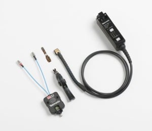
Use the low loading, Tektronix TDP7700 (for 6 Series and 6 Series B MSO) or P7700 (for 70000 C/DX/SX Oscilloscopes) Series High Impedance TriMode probe to measure MIPI signals
Supports TekFlex™ accessories for flexible probing
Offline and remote analysis
- Analyze live or pre-acquired waveforms
- Allows remote execution of tests
Key features (version 2.1)
- Support Spread Spectrum Clocking enabled / disabled measurements. Triangular Down spreading, deviation 5000ppm at 33 kHz
- Transmitter eye diagram (Test ID 1.5.7) at data rates > 1.5 Gbps and ≤ 4.5 Gbps measurement using random test pattern of 3 million UI
- Support Horizontal mask movement. Data eye mask can be moved from center of DDR clock with 0 V crossing up to ±0.1UI range to eliminate data to clock skew effects
- Support three reference templates (Short, Standard, and Long) for differential insertion loss for data rates > 1.5 Gbps and ≤ 4.5 Gbps
- Mask prorated to BER 10e-6, with TEYE_TX = 0.53 UI and VDIF_TX 47 mV
- Option to run tests in Compliance Mode or with user defined settings
Applications
- Automotive cameras
- Automotive infotainment and dashboard displays
- Mobile camera and displays
- Large tablets
- Smart watches
Single-button fully automated D-PHY testing
The Tektronix TekExpress D-PHY application runs on 6 Series and 6 Series B MSO with Option 6-WIN installed (Windows 10 operating system) and DPO/MSO 70000 DX/SX Series Oscilloscope. The close integration of the oscilloscope and test software provides an automated, simple, and efficient way to test D-PHY transmitter interfaces and devices consistent to the requirements of the D-PHY Conformance Test Specification version 2.1.
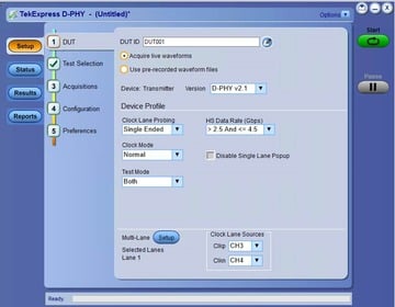
Measurement setup and test execution is simple with the D-PHY software. The intuitive Graphical User Interface (GUI) is laid out to represent the workflow from setup through testing, letting you focus on design and debug instead of setting up the measurements.

Simply select tests from the menu for HS, LP, and HS-LP groups as per specifications.
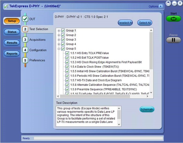
You can view the schematic of the selected test with a push of a button. You can also display a test connection diagram to avoid setup errors.
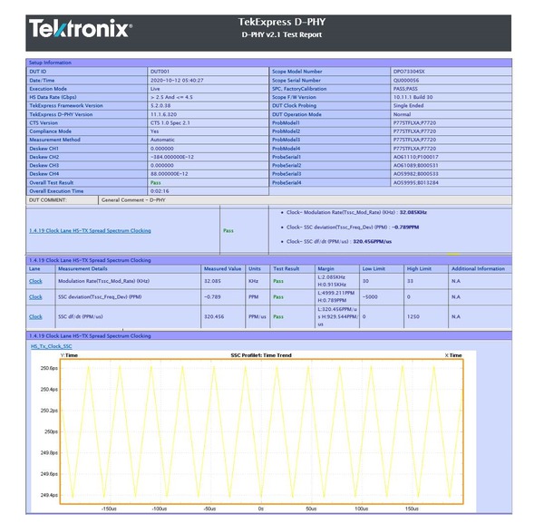
Pass/Fail report
The report tab provides a view of the complete test results, pass or fail status, test margin, and images supporting the test results, for each lane of the DUT.
TDP7700/P7700 series TriMode probes for MIPI D-PHY TX measurements
MIPI D-PHY applications have special probing requirements due to the different signal measurement sources in High Speed and Low Power modes. In High Speed mode, D-PHY signals operate in terminated mode with differential signaling. In Low Power mode, D-PHY signals operate in unterminated mode with single-ended signals. Therefore, MIPI D-PHY has two key probing requirements:
- Provide a high impedance to minimize signal loading
- Need both Differential and single-ended mode probing
The Tektronix TDP7700/P7700 Series TriMode probes are designed to meet this measurement challenge. The TDP7700/P7700 work with full AC calibration of the probe and tip's signal path, to provide the highest probe fidelity available for real-time oscilloscopes. The innovative new probe design uses SiGe technology to provide the bandwidth and fidelity needed today and in the future.
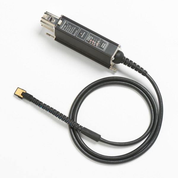
A key TDP7700/P7700 connectivity innovation is using solder-down probe tips with the probe's input buffer mounted only a few millimeters from the tip. This approach provides unmatched usability for connecting to MIPI D-PHY circuits.
Other TDP7700/P7700 Series probe characteristics include:
- An active buffer amplifier on the probe tips with the probe input only 3.2 mm from the buffer.
- Excellent step response and low insertion loss up to 20 GHz on P7720
- Low-DUT loading with 100 kΩ (DC) and 0.4 pF (AC) performance
- High Common-Mode Rejection Ratio (CMRR)
- Low noise
Specifications
- D-PHY specification
- Version 1.2 and Version 2.1
- D-PHY CTS
- Version 1.0
- Measurements
- Both High Speed and Low Power modes, including ULPS and BTA.
- Group 1 tests
- Data lane LP-TX signaling
- 1.1.1
- Data lane LP-TX Thevenin output high level voltage (VOH)
- 1.1.2
- Data lane LP-TX Thevenin output low level voltage (VOL)
- 1.1.3
- Data lane rise time
- 1.1.4
- Data lane fall time
- 1.1.5
- Data lane LP-TX slew rate versus CLOAD (δV/δtSR)
- 1.1.6
- Data lane LP-TX pulse width of exclusive-OR clock (TLP-PULSE-TX)
- 1.1.7
- Data lane LP-TX period of exclusive-OR clock (TLP-PER-TX)
- Group 2 tests
- Clock lane LP-TX signaling
- 1.2.1
- Clock lane LP-TX Thevenin output high level voltage (VOH)
- 1.2.2
- Clock lane LP-TX Thevenin output low level voltage (VOL)
- 1.2.3
- Clock lane rise time
- 1.2.4
- Clock lane fall time
- 1.2.5
- Clock lane LP-TX slew rate vs. CLOAD (δV/δtSR)
- Group 3 tests
- Data lane HS-TX signaling
- 1.3.1
- Data lane HS entry: data lane TLPX value
- 1.3.2
- Data lane HS entry: THS-PREPARE value
- 1.3.3
- Data lane HS entry: THS-PREPARE + THS-ZERO value
- 1.3.4
- Data lane HS-TX differential voltages (VOD(0), VOD(1))
- 1.3.5
- Data lane HS-TX differential voltage mismatch (ΔVOD)
- 1.3.6
- Data lane HS-TX single ended output high voltages (VOHHS(DP), VOHHS(DN))
- 1.3.7
- Data lane HS-TX common-mode voltages (VCMTX(1), VCMTX(0))
- 1.3.8
- Data lane HS-TX common-mode voltage mismatch (ΔVCMTX(1,0))
- 1.3.9
- Data lane HS-TX dynamic common-level variations between 50-450 MHz (ΔVCMTX(LF))
- 1.3.10
- Data lane HS-TX dynamic common-level variations above 450 MHz (ΔVCMTX(HF))
- 1.3.11
- Data lane HS-TX 20%-80% rise time (tR)
- 1.3.12
- Data lane HS-TX 80%-20% fall time (tR)
- 1.3.13
- Data lane HS exit: THS-TRAIL value
- 1.3.14
- Data lane HS exit: 30%-80% Post-EoT rise time (TREOT) value
- 1.3.15
- Data lane HS exit: TEOT value
- 1.3.16
- Data lane HS exit: THS-EXIT value
- Group 4 tests
- Clock lane HS-TX signaling
- 1.4.1
- Clock lane HS entry: TLPX value
- 1.4.2
- Clock lane HS entry: TCLK-PREPARE value
- 1.4.3
- Clock lane HS entry: TCLK-PREPARE + TZERO value
- 1.4.4
- Clock lane HS-TX differential voltages (VOD(0), VOD(1))
- 1.4.5
- Clock lane HS-TX differential voltage mismatch (ΔVOD)
- 1.4.6
- Clock lane HS-TX single ended output high voltages (VOHHS(DP), VOHHS(DN))
- 1.4.7
- Clock lane HS-TX common-mode voltages (VCMTX(1), VCMTX(0))
- 1.4.8
- Clock lane HS-TX common-mode voltage mismatch (ΔVCMTX(1,0))
- 1.4.9
- Clock lane HS-TX dynamic common-level variations between 50-450 MHz (ΔVCMTX(LF))
- 1.4.10
- Clock lane HS-TX dynamic common-level variations above 450 MHz (ΔVCMTX(HF))
- 1.4.11
- Clock lane HS-TX 20%-80% rise time (tR)
- 1.4.12
- Clock lane HS-TX 80%-20% fall time (tR)
- 1.4.13
- Clock lane HS exit: TCLK-TRAIL value
- 1.4.14
- Clock lane HS exit: 30%-80% Post-EoT rise time (TREOT) value
- 1.4.15
- Clock lane HS exit: TEOT value
- 1.4.16
- Clock lane HS exit: THS-EXIT value
- 1.4.17
- Clock lane HS clock instantaneous (UIINST)
- 1.4.18
- Clock Lane HS Clock Delta UI (ΔUI)
- 1.4.19
- TX Spread Spectrum Clocking (SSC) Requirements
- 1.4.20
- Clock Lane HS Clock Period Jitter
- Group 5 tests
- HS-TX Clock-to-Data lane timing
- 1.5.1
- HS entry TCLK-PREValue
- 1.5.2
- HS exit TCLK-POST value
- 1.5.3
- HS clock rising edge alignment to first payload bit
- 1.5.4
- Data-to-Clock skew (TSKEW (TX))
- 1.5.5
- Initial HS Skew Calibration Burst (TSKEWCAL-SYNC, TSKEWCAL)
- 1.5.6
- Periodic HS Skew Calibration Burst (TSKEWCAL-SYNC, TSKEWCAL)
- 1.5.7
- HS-TX Data and Clock Eye Diagram
- 1.5.8
- Alternate Calibration Sequence (TALTCAL-SYNC, TALTCAL)
- 1.5.9
- Preamble Sequence (TPREAMBLE, TEXTSYNC)
- 1.5.10
- Clock and Data Lane TX HS-Idle: THS-IDLE-POST, THS-IDLE-CLKHS0, THS-IDLE-PRE Values
- Group 6 tests
- LP-TX INIT, ULPS and BTA requirements
- 1.6.1
- INIT: LP-TX initialization period (TINIT, MASTER)
- 1.6.2
- ULPS entry: verification of clock lane LP-TX ULPS support
- 1.6.3
- ULPS exit: transmitted TWAKEUP interval
- 1.6.4
- BTA: TX-Side TTA-GO interval value
- 1.6.5
- BTA: RX-Side TTA-SURE interval value
- 1.6.6
- BTA: RX-Side TTA-GET interval value
- Probing configuration
- Single-ended and differential acquisition. Conformance requires DP, DN, CP, and CN. One lane is two wires, two single ended probing. In case of continuous clock, a single probe may be used in differential mode.
- Multilane
- The TekExpress application will perform testing one lane at a time in sequential order, a popup message appears which ask the user to change the physical connection to next data lanes.
- Triggering
- Edge trigger for clock lane tests in clock continuous mode. Choice of width trigger and transition trigger for all other tests and all other modes .
- Reports
- CSV, PDF, and MHT formats with images of all acquired waveforms.
Ordering information
Required hardware
Models
| D-PHY v1.2 | D-PHY v2.1 | |
|---|---|---|
| CTS | 1.0 | 1.0 |
| CTS compliance | Minimum bandwidth of 8 GHz on oscilloscope | Minimum bandwidth of 13 GHz on oscilloscope |
| DJA/6-DJA | Optional Test ID 1.5.4 Eye diagram display required DJA. In the absence of DJA, gives the measured value alone. | Mandatory |
| Oscilloscope models | MSO/DPO 70000 DX | MSO/DPO 70000 DX |
| DPO/DPS 70000 SX (4 Ch Models) | DPO/DPS 70000 SX (4 Ch Models) | |
| MSO/DPO 70000 C (4 GHz and above) | ||
| 6 Series and 6 Series B MSO (2.5 GHz and above with 6-WIN) | 6 Series and 6 Series B (2.5 GHz and above with 6-WIN) Minimum recommended bandwidth on 6 Series and 6 Series B is 4 GHz. However, the application installs on 6 Series and 6 Series B with bandwidth 2.5 GHz |
Required software
| Application | Option | License type |
|---|---|---|
| MIPI D-PHY 1.2 Automated Compliance Solution on 6 Series and 6 Series B oscilloscopes. 6-DJA is required for Test ID1.5.4. 6-DJA is optional. | 6-CMDPHY | New instrument license |
| SUP6-CMDPHY | Upgrade license | |
| SUP6-CMDPHY-FL | Floating license | |
| MIPI D-PHY 2.1 Automated Compliance Solution on 6 Series and 6 Series B MSO with 6-DJA enabled. 6-DJA is mandatory | 6-CMDPHY21 | New instrument license |
| SUP6-CMDPHY21 | Upgrade license | |
| SUP6-CMDPHY21-FL | Floating license |
| Application | Option | License type |
|---|---|---|
| MIPI D-PHY 1.2 Automated Compliance Solution on 70000 C, DX, and SX oscilloscopes. Opt.DJA is required for Test ID1.5.4. DJA is optional | DPHY12 | New instrument license |
| DPO-UP DPHY12 | Upgrade license | |
| DPOFL-DPHY12 | Floating license | |
| MIPI D-PHY 2.1 Automated Compliance Solution on 70000 DX and SX oscilloscopes with Opt. DJA enabled. DJA is mandatory | DPHY21 | New instrument license |
| DPO-UP DPHY21 | Upgrade license | |
| DPOFL-DPHY21 | Floating license |
Recommended probes
| Oscilloscope | Probe | Quantity |
|---|---|---|
| 6 Series and 6 Series B MSO | TDP7708 Series Tri-mode probe with P77STFLXA solder−in tip with TekFlex connector technology | Four (recommended for connecting Dp, Dn, Cp, and Cn) |
| DPO/MSO70000 C/DX/SX Series | P7700 Tri-mode probe with P77STFLXA solder-in tip with TekFlex connector |
Recommended test fixtures
| Text fixtures | Vendor |
|---|---|
| D-PHY Reference Termination Board | UNH-IOL |

Tektronix is registered to ISO 9001 and ISO 14001 by SRI Quality System Registrar. Product(s) complies with IEEE Standard 488.1-1987, RS-232-C, and with Tektronix Standard Codes and Formats. Product Area Assessed: The planning, design/development and manufacture of electronic Test and Measurement instruments. 61W-61487-6