1. Introduction
Error Location Analysis is a powerful but underused tool that can give designers, test engineers, and technicians a huge hardware debug advantage. In this paper we present Error Location Analysis from a hands-on perspective in the context of analyzing the high speed serdes used in systems like 100G and 400G Ethernet, PCIe 3 and 4, SAS 3 and 4, and USB 3.1—high performance 10+ Gb/s serdes that depend on clock recovery and equalization to meet BER (bit error rate) requirements in the presence of jitter, noise, and crosstalk, while under the pressure of eye-closing insertion loss, return loss, and ISI (inter-symbol interference).
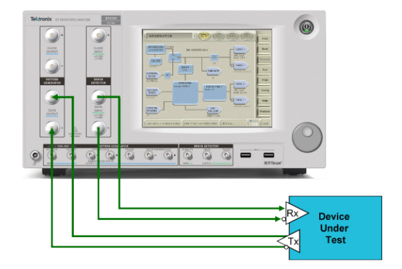
Error Location Analysis transforms sophisticated BERTs (bit error ratio testers) like Tektronix’s BSA-series and BSX-series BERTScopes into advanced component analysis engines.
The idea is straightforward and the potential is as wide as your imagination: Bit errors occur when system components are stressed beyond their performance margins. The locations of those bit errors—their order in time, where they occur in the test pattern, whether they come in bursts and the lengths of those bursts, whether or not they correlate to system time-scales or block sizes—betray which component or components are at fault. The trick is to combine a test pattern with signal impairments that target specific components within the system and then watch for characteristic patterns in the resulting distributions of those errors.
In the next few pages, we’ll lay out simple strategies to illustrate the power of virtual probing with precision stress and Error Location Analysis. We’ll touch on transmitter testing but focus on receiver testing since the performance of high speed serial data systems rely on complex receivers that are notoriously difficult to debug.
Since you know your design, your system, and your components better than anyone, consider this strategy a starting point. As you develop experience combining signal stresses, test patterns, and error distributions, you’ll develop formidable debug prowess.
2. Virtual Probing High Speed Serdes
Error Location Analysis starts with the BERT error detector’s ability to identify and log the precise positions of all errors in a data stream.
Figure 1 shows a BERT’s essential components: the BERT pattern generator transmits a repeating test signal to a test receiver. Error Location Analysis requires that the receiver operate in loopback mode so that the BERT error detector can identify and log errors in the retimed receiver output.
The Strip Chart is the simplest form of Error Location Analysis: a constantly updating graph of error occurrences, BER, or burst errors and the relative contributions of burst and bit errors.
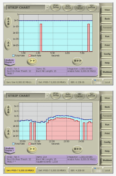
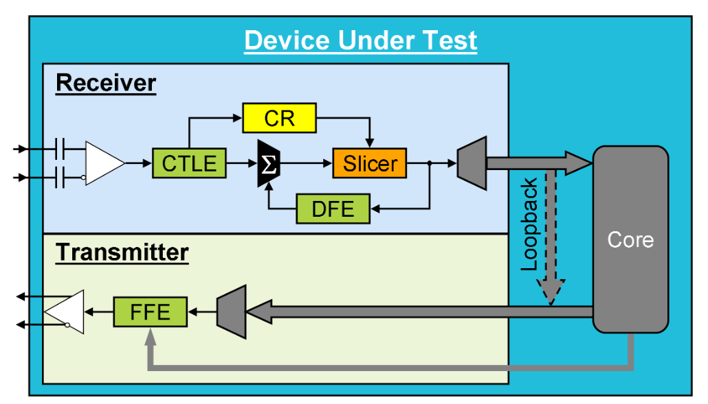
Figure 3 shows a typical serdes architecture. A differential signal enters the receiver through an AC coupled input to a comparator followed by a CTLE (continuous time linear equalizer). The signal is split with one leg going to the CR (clock recovery) circuit and the other to the logic-decoding voltage slicer. The recovered clock sets the time-delay position for the voltage slicer. The symbol decisions emerge from the voltage slicer and this retimed signal is split, with one output continuing to the serdes core and the other fed back to the DFE (decision feedback equalizer). The output of the DFE is added to the CTLE output and on to the voltage slicer. When in loopback mode, the retimed slicer output bypasses the core and is looped back to the serdes transmitter.
The serdes transmitter is driven by a data-rate clock derived from a low rate reference clock multiplied up to the data rate by a PLL (phase-locked loop). The serialized signal is then modified by the transmitter’s FFE (feed-forward equalizer).
Since the serdes consists of integrated components that cannot be probed, it is essentially a black box. The transmitted signal can be analyzed on oscilloscopes with eye diagrams, jitter and noise tools, and waveform analysis, but the situation for the receiver is much more difficult. In high speed serial systems, the eye diagram at the receiver is closed and the only way to evaluate the performance of the CTLE, CR, and DFE is to imagine their inputs through modeling. To measure the performance of each internal component we target them with carefully chosen test pattern and signal stress combinations.
Virtual probing with precision stress and Error Location Analysis is a process of elimination. Start with a pristine signal transmitted through high quality matched cables that delivers a wide open eye to the receiver input and the untroubled receiver operates with ease. We then stress each component to their limits. When they reach those limits the resulting errors follow patterns that, with Error Location Analysis tools, we can trace back to root causes.
2.1 PROBING FORWARD ERROR CORRECTION
FEC (forward error correction) offers design flexibility in severe operating environments at the expense of increased overhead, latency, and power by relaxing the raw BER performance requirements, but it’s no panacea.
FEC adds parity-like bits to signal bits. The data and parity bits form blocks that are encoded by a shift register in such a way that, at the receiver, a complementary shift register can decode the word and correct some bit errors. The number of bits that an FEC scheme can correct depends on the order of the errors within each block (in the language of FEC what we’re calling blocks are referred to as codewords). If the number of errors exceeds that capacity of the FEC scheme, none of them can be corrected.
The order dependence of the FEC performance makes it impossible to predict the post FEC BER from the raw, pre-FEC BER without Error Location Analysis. To ease the interpretation Reed-Solomon FEC, the most common scheme, Tektronix offers an FEC Emulation tool that is built on Error Location Analysis.
FEC schemes operate on fixed blocks of data. The Block Error Histogram shows the number of errors that occur in blocks. Since the maximum number of correctable errors depends on how many occur in each block, it’s easy to translate the raw BER to the FEC-corrected BER with Block Error Histograms. As shown in Figure 4, FEC Emulation translates raw system performance to FEC performance including the error count, BER, and data rate.
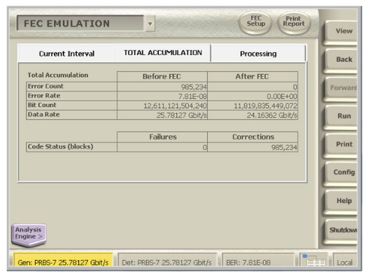
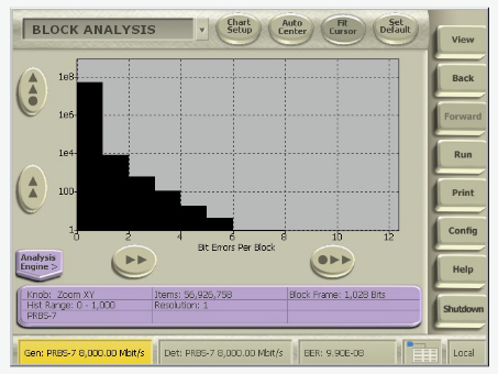
A Block Error Histogram shows the number of errors that occur in blocks of data. The block size should be defined as a length scale like the number of bits that make up a codeword, packet size, frame, or disk sector. The analyzer counts the number of errors that occur in each block and provides the histogram of number errors per block.
A smooth Block Error Histogram may result from random errors, but spikes in the histogram indicate systematic performance problems. Combining analysis of the Block Error Histogram and the Correlation Analysis Histogram with correlation length set to the same block length, you can determine whether the errors occur at specific locations within the block.
Since burst errors adversely affect FEC performance, many systems interleave data at the receiver. Interleaving shuffles bit errors across blocks, reduces the likely number of errors per block, and increases FEC performance. FEC Emulation can easily be configured to accommodate any interleaving or data striping system.
FEC Emulation also allows designers to optimize the tradeoffs between an FEC scheme’s effective SNR improvement and its costs in bandwidth overhead, latency, and power without having to implement the actual FEC mathematics in simulation or hardware.
2.2 PROBING THE MULTIPLEXER AND DEMULTIPLEXER
We start with the serdes mux/demux core. Mux/de-mux problems generate errors strongly correlated to the multiplexer width.
Start with a clean signal, no applied impairments, and a simple but nontrivial test pattern, say PRBS7—plenty of edges for the CR, but complex enough to distinguish each mux channel.
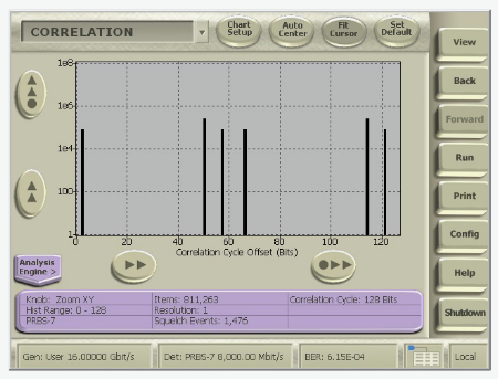
Problems associated with a certain scale like multiplexer width, interleaving depth, packet or block size, etc, can be identified with the Correlation Analysis Histogram. Set the correlation length to the multiplexer width and errors caused by a faulty mux channel accumulate in an isolated peak in the Correlation Analysis Histogram.
A Correlation Analysis Histogram shows how the locations of errors correlate to user-set correlation lengths like block size, system timescales measured in bits, or an external marker signal. The correlation length defines the number of bins in the correlation histogram before wrap-around. The correlation analysis histogram gives the number of error occurrences positioned at modulo the correlation length.
2.3 PROBING THE AC COUPLED DIFFERENTIAL INPUT
If the average signal voltage varies over a significant timescale, then the baseline voltage will wander. The significant timescale is set by the AC coupling RC time constant, TAC, which is usually specified by the standard.
To stress the AC coupled input, use a test pattern with long segments of high and low mark density. The mark density is the average fraction of logic ones in the data. The standards require a mark density of ½; that is, equal numbers of ones and zeros averaged over a time scale shorter than the AC coupling time constant.
To isolate the AC coupled input performance from the CR performance, the stress pattern should include plenty of clock content in the form of logic transitions. For example, a signal like 1111 1110 repeated many times has both sufficient transition density to satisfy the CR and the low mark density needed to stress the AC coupled input. To re-stabilize the receiver, follow the high mark density sequence with a pattern that’s easy for both the AC-coupled input and CR, like several repetitions of PRBS5:
(1111 1110)•n, (PRBS5+PRBS5-complement)•n,(0000 0001)•n, (PRBS5+PRBS5-complement)•n
Start with values of n that are significantly lower than the AC coupling time constant, i.e., n << fdTAC where fd is the data rate.The receiver should perform error free until the imbalanced pattern sequences exceed the AC coupling time constant.
Increase n until you start to see errors; expect burst errors at the onset of the PRBS5 sequences with more errored 1s than errored 0s in the first PRBS sequence and vice versa in second. Check whether or not the receiver behaves the same way after the long run of low mark density as it does after high mark density; an asymmetry could mean imbalance in the input coupling and/or in the voltage slicer threshold.
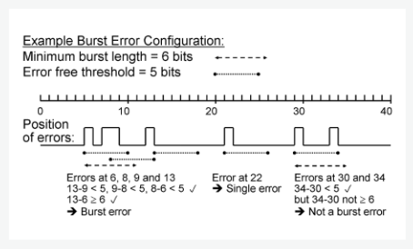
Burst errors are defined by two Error Location Analysis parameters: the minimum burst length and the error free threshold. The minimum burst length determines the minimum number of bits in a burst error but not the minimum number of errors in that burst.
A burst of errors occurs any time there are two or more errors closer together than the error free threshold. The number of errors in a burst error is different than the number of burst errors or the burst error rate.
Let’s work through it. Say errors occur successively at positions i, j, and, k. The three errors form a burst if the separation between each of them is less than the error free threshold and the separation between the two that are farthest from each other is less than or equal to the minimum burst length:
Situation: errors located at i, j, and, k sequentially so that i < j < k.
The three form a burst error of length k – i if
(j – i < error free threshold) and
(k – j < error free threshold) and
(k – i ≥ minimum burst length).
Common mode interference could also aggravate the AC coupled differential input if it’s imbalanced. Double check the test fixture skew. With a robust pattern like PRBS7 or PRBS9, apply increasing levels of CMSI (common mode sinusoidal interference). The comparator input should have no trouble canceling common mode noise.
2.4 PROBING THE CLOCK RECOVERY CIRCUIT
The clock recovery circuit uses the logic transitions of the input waveform to synthesize and lock a data-rate clock. The more logic transitions, the more clock content in the signal, the easier it is for the CR.
In this section we’ll discuss two ways to probe CR performance. The first is a direct probe of the ability of the CR to recover and lock and the second probes the CR bandwidth and its ability to track jitter.
2.4.1 Testing CR Lock Margin
To assure sufficient clock content, standards 50% transition density and limit the maximum allowed runs of CIDs (consecutive identical bits) through a combination of data encoding and scrambling. Data encoding schemes vary for different standards, for example, 100G Ethernet uses 64B/66B encoding, PCIe Gen 4 uses 128B/130B, and SAS Gen 4 uses 128B/150B. Scrambling reduces the probability of CID runs longer than about 32 bits to less than one in a trillion.
To probe the CR we put CID strings in the test pattern that challenge its ability to lock and hold the clock signal.
Long runs of CIDs have imbalanced mark density which can also stress the AC coupled input. Prior to probing the clock recovery test, make sure that the differential AC coupled input is robust to drift over sequences longer than the CID sequences used to stress the CR.
To stress the receiver, start with a test pattern with plenty of clock content, like PRBS5 or PRBS7, and then add CID sequences like:
(1111)•n, (PRBS5+PRBS5-complement)•n,(0000)•n, (PRBS5+PRBS5-complement)•n
Start with small n and increase it until you see errors; call that value ncrit which needn’t be exact. When the clock loses lock, the timing of the voltage slicer starts to wander and, depending on CR design, you can expect burst errors during the PRBS sequences of the pattern.
The value of ncrit should be substantially longer than the longest CID run in the receiver compliance test pattern, usually 32 bits. If ncrit ~ 32 bits, the CR is operating at the edge of its margin and is likely to lose lock in the presence of other signal impairments like ISI or PJ.
2.4.2 Testing CR Jitter Filter Bandwidth
The second CR test is a key part of compliance stressed receiver tolerance tests, but by using Error Location Analysis, you can zero in on the CR performance.
To probe the CR bandwidth, BWCR, apply SJ (sinusoidal jitter) of varying frequencies and amplitudes to a test pattern with plenty of transitions like PRBS7 or PRBS9. The idea is to stress the CR bandwidth and its ability to filter jitter independent of its ability to lock. Start with low frequency, fSJ << BWCR and high amplitude SJ, like that shown in Figure 8. Increase the amplitude until the BER ramps up, call that amplitude Acrit(fSJ). Continue across the template, making careful measurements through the CR roll off.
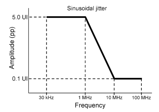
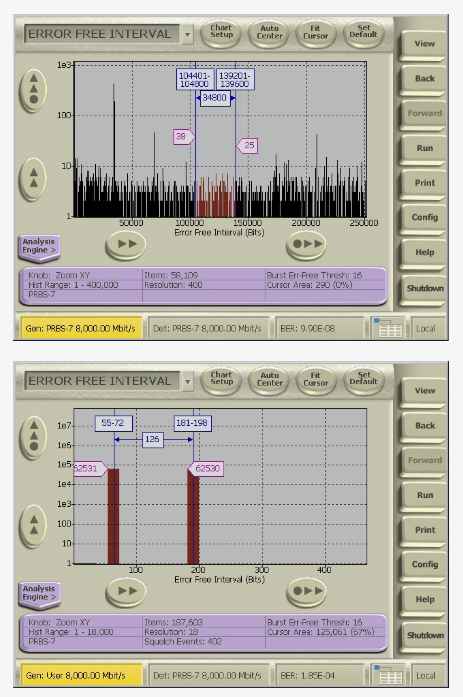
To confirm that errors are being caused by the CR failing to filter jitter at Acrit(fSJ), analyze the Error Free Interval histogram.
Expect errors at both the maxima and minima of SJ oscillations. The period of the SJ oscillation is TSJ = 1/fSJ, or measured in bit intervals, nSJ ~ Tbit/TSJ = Tbit fSJ. Errors caused by SJ appear as clumps twice per bit period or at ½ nSJ in the Error Free Interval Histogram.
The Error Free Interval Histogram gives the number of times that errors are separated by error free intervals.
Systematic and deterministic errors tend to occur at intervals: periodic jitter and noise cause maximum signal impairments twice each period, inter-symbol interference causes errors around at points in the pattern, trouble with multiplexers and demultiplexers is likely to repeat at the mux width, etc. Random errors also have typical signatures in the error free interval histogram.
2.5 PROBING EQUALIZER PERFORMANCE AND CLOSED EYE DIAGRAMS
Equalization inverts the channel response to reduce ISI and open the eye for the voltage slicer.
Each logic transition in a waveform traces an average “trajectory,” from 0 to 1, 0 to 0, 1 to 0, or 1 to 1. The number of unique trajectories is given by the number of permutations of bit transitions over the length of its pulse response. For example, if the pulse response—the waveform of a single high symbol in a long run of low symbols (think of …0001000…) is 3 bits long, then the number of unique trajectories is given by the number of permutations of 3 bits, 32 = 9; if the pulse response extends over 4 bits, there are 42 = 16 unique trajectories. Since the pulse response approaches the 0 rail asymptotically, in principle it can be arbitrarily long; in practice, the pulse response of 10+ Gb/s signals can extend over dozens of bits. An exhaustive test of equalizer performance would stress the receiver with every bit sequence that extends over the length of the pulse response.
In the absence of other signal impairments, errors caused by ISI occur on the same bits in each repetition of the test pattern;that is, they are correlated to the pattern.
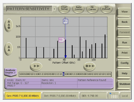
There are several ways to use Error Location Analysis to identify pattern-dependent errors like ISI. First, Pattern Sensitivity Analysis yields a histogram that shows the number of errors at every bit position in the pattern.
The Pattern Sensitivity Analysis Histogram charts the number of errors at each position in the test pattern.
Errors that are correlated to the test pattern those caused by ISI or DDJ (data-dependent jitter), a mix of ISI and F/2 (a type of duty cycle distortion) jitter accumulate in peaks in the pattern sensitivity analysis histogram. If the errors are uncorrelated to the data, that is, if they’re not pattern sensitive, then they accumulate throughout the pattern. Errors caused by jitter accumulate at bits that follow logic transitions and errors caused by voltage noise can happen anywhere in the pattern.
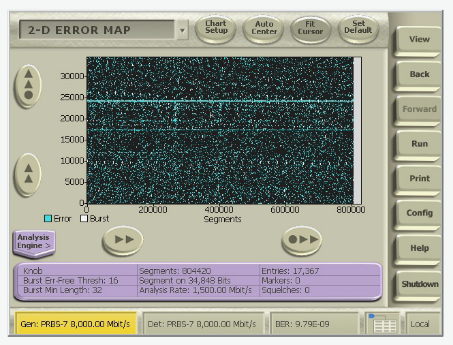
The Error Map is a two dimensional representation whose characteristics must be configured for specific situations. The incoming signal is separated into sequential blocks. Errors are indicated by lit pixels whose vertical position indicates their position in a block and whose horizontal position indicates which block they’re in.
The vertical axis/block length should be defined in terms of a scale-factor for the system you’re analyzing; to diagnose pattern sensitive or correlated errors, a good choice for the vertical axis is the length of the pattern. If you’re analyzing a system that operates with a specific block length like the length of packets or codewords associated with an FEC (forward error correction) scheme that block length makes a good choice for the vertical axis.
Burst errors and bit errors are plotted in different colors, so you also have to define burst errors in terms of the minimum burst length and error free threshold.
For example, Figure 11 shows an error map with vertical axis set to the pattern length. Horizontal lines indicate errors that occur at the same position in the pattern on every repetition.
Second, ISI shows up as peaks at fixed intervals in the Error Free Interval Histogram. ISI that only causes an error at the most difficult bit transition in a pattern shows up as a peak at the pattern length.
A third technique is to study the 2D Error Map with vertical scale/block length set to the length of the test pattern; pattern sensitive/correlated errors form patterns that jump out at you.
2.5.1 Probing the CTLE
Since the CTLE gain is defined by the channel response, we probe it with ISI stress generated by the channel for which it should have been optimized and vary the level of ISI stress by using different test patterns. Since the CTLE performance directly affects the CR and DFE performance, and since CR and DFE failures both tend to result in burst errors, one way to isolate the CTLE is to find a test pattern that results in just a few pattern sensitive bit errors.
To search for the pattern sensitivity threshold monitor the Pattern Sensitivity Histogram or the error map with block size defined by the pattern length. Start with a very simple pattern: a repeating clock-like signal 0101.This signal experiences channel loss but not ISI since it includes at most a few Fourier components: predominantly the fundamental harmonic at fd/2, a low amplitude contribution at 3fd/2, and perhaps a trace at 5fd/2. If there are no errors, then switch to a very challenging pattern like JTPAT the jitter tolerance pattern designed to generate the maximum ISI in a pattern that’s just 2240 bits long by the Fibre Channel MJSQ (Methodologies for Jitter and Signal Quality Specification) group.
If the burst error rate jumps up indicated by errors accumulating after certain sequences in the Pattern Sensitivity Histogram or an increase in pattern sensitive burst errors in the Error Map—the problem could be caused by any combination of the CTLE and DFE. To isolate the CTLE, try another low ISI pattern, say PRBS7. Continue alternating between high and low ISI patterns until you find a pattern that generates bit errors rather than burst errors.
If the CTLE filter varies from the required response shown in Figure 12, then expect pattern sensitive bit errors to show up as isolated peaks in the Pattern Sensitivity Histogram or bit errors but not burst errors in rows on the Error Map.
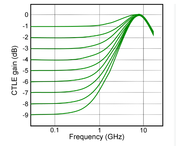
To distinguish whether the CTLE problem is due to inappropriate gain or incorrect filter shape, repeat the analysis with different test boards and the CTLE gain tuned for each board. If bit errors occur at pattern positions that are not worst case ISI triggers, like runs of CIDs followed by isolated transitions, the CTLE filter shape probably varies from that shown in Figure 12; if bits follow likely ISI triggers then the CTLE gain isn’t properly optimized.
2.5.2 Probing the DFE
DFE is a nonlinear IIR (infinite impulse response) filter. Since it feeds back previous decisions of the voltage slicer, bit errors corrupt its feedback which causes burst or avalanche errors.
Assuming the CTLE and CR have been checked, repeat the process outlined for probing the CTLE to find the critical level of ISI where errors start to occur. The obvious signature for DFE failure is the onset of burst errors in a Pattern Sensitivity Histogram at worst-case ISI-generating bit sequences or burst errors that show up in rows on the Error Map.
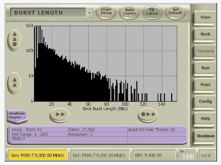
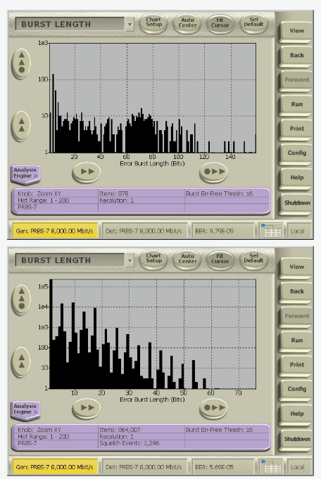
To confirm that the problem is caused by the DFE, look at the Burst Length Histogram. Since DFE burst errors occur on every pattern repetition and have the same burst length every time (in the absence of other signal impairments), look for a nearly fixed burst length, just a few adjacent columns in the Burst Length Histogram.
A Burst Length Histogram shows the number of occurrences of burst errors of different lengths. Burst errors depend on your definition of minimum burst length and error free interval. The Burst Length Histogram is most useful when you define small minimum burst lengths. Peaks in the histogram indicate systematic problems that generate fixed-length error avalanches like interference or failing DFEs.
3. Error Location Analysis in Stressed Receiver Compliance Tests
Stressed receiver compliance tests, also called jitter stress tests or interference tolerance tests, apply several stresses to the receiver at once. The idea is to submit the receiver to the worst case compliant conditions. If it can operate at the required BER in the worst case conditions then it should be able to operate with any combination of other compliant serdes and channels.
The applied stresses include some or all of
- RJ (random jitter)
- ISI
- SJ, usually across a template like that shown in Figure 8
- DMSI (differential mode sinusoidal interference)
- CMSI (common mode interference)
It’s difficult to diagnose specific problems when so many stresses are applied at once, but we can get hints.
Since jitter only causes errors at bit transitions, RJ (random jitter) causes errors that occur at random logic transitions. RN (random noise) on the other hand, can cause errors anywhere, though it’s more likely to cause them in the presence of other causes of vertical eye closure like ISI or sinusoidal interference.
In the absence of other stresses, errors caused by random processes follow specific statistical distributions. Since random errors follow Gaussian statistics, they tend to occur as isolated single errors, we expect the Burst Length Histogram for random jitter and noise to peak at one with exponentially fewer at two and so on. Since they’re not correlated to the pattern, random errors form a continuum in the Pattern Sensitivity Analysis Histogram; similarly, since they aren’t correlated to any particular time scale, random errors also form a continuum in the Error Free Interval Histogram.
PJ (periodic jitter) and PN (periodic noise) that can be caused by EMI (electromagnetic interference) appears as clumps in the Error Free Interval histogram with block size set to the timedelay of the period (or half the period) of any oscillators.
In a tolerance test with several stresses, errors caused by PJ and PN appear as spikes above a smooth continuum of random errors in the Error Free Interval Histogram.
4. Conclusion
Combining a sophisticated BERT’s ability to apply a wide variety of stressful patterns and precise levels of signal stressors with Error Location Analysis provides powerful, actionable debug information.
By starting with clean signals and then applying combinations of well considered test patterns and signal impairments, the performance of individual components that are integrated into serdes chips can be tested. Since the only indicator of serdes receiver performance comes from errors, the locations and timing of bit errors and burst errors with respect to each other, with respect to the test pattern, with respect to a block or packet size or any other scale, offers insight into the causes of those errors.
Error Location Analysis reveals the causes of errors in many ways with these tools:
- Basic BER Analysis: a tabular display of bit and burst error counts and rates.
- Strip Chart Analysis: a scrolling graph of error occurrences, updating as measurement progresses with the proportions of burst and bit errors.
- FEC Emulation: provides both the raw BER and the FECcorrected BER for any FEC scheme you might want to test or audition including schemes that use interleaving and data striping.
- Block Error Analysis: a histogram of the number of times blocks of a defined length have occurred with specific numbers of errors.
- Pattern Sensitivity Analysis: a histogram of the number of errors at each position of the test pattern bit sequence.
- Correlation Analysis: a histogram showing how error locations correlate to user-set block sizes or external Marker signal inputs.
- Error Free Interval Analysis: a histogram of the number of occurrences of different error free intervals.
- Burst Length Analysis: a histogram of the number of occurrences of burst errors of different lengths.
- Error Map Analysis: a two-dimensional representation of error location data.
You can see from the few examples we’ve touched on here that these analysis tools can be combined to isolate even the most intractable bugs.
Error Location Analysis is exclusively available on Tektronix’s BERTScopes, Figure 14.