The Semiconductor Characterization Challenge
Engineers and researchers are constantly challenged to create new semiconductor technologies or processes or improve existing ones. Whether the challenge is designing a lower power front end for a next-generation smartphone or investigating new materials for high efficiency solar panels, you need test tools and techniques that support making precise electrical measurements with high accuracy and efficiency.
This e-guide answers some common questions about making better semiconductor measurements, with a focus on DC I-V and capacitance-voltage (C-V) measurements. It also touches on more specific applications and how you can simplify making the measurements your most challenging applications require.
COMMON SEMICONDUCTOR TEST OBJECTIVES
- Semiconductor designer specification tests
- To ensure the device meets its required power specifications
- To determine if the device behaves as anticipated across its full range
- To confirm the device does not exhibit dangerous behavior under any conditions
- Materials researcher tests
- To investigate sample degradation or failure
- To determine sample purity
- To check a material’s uniformity
Diagnosing Common Semiconductor Testing Errors
I know there are errors in my lowlevel DC measurements, but how can I identify and eliminate them?
Each type of low-level measurement is subject to different kinds of error sources, but here are some tips that can help.
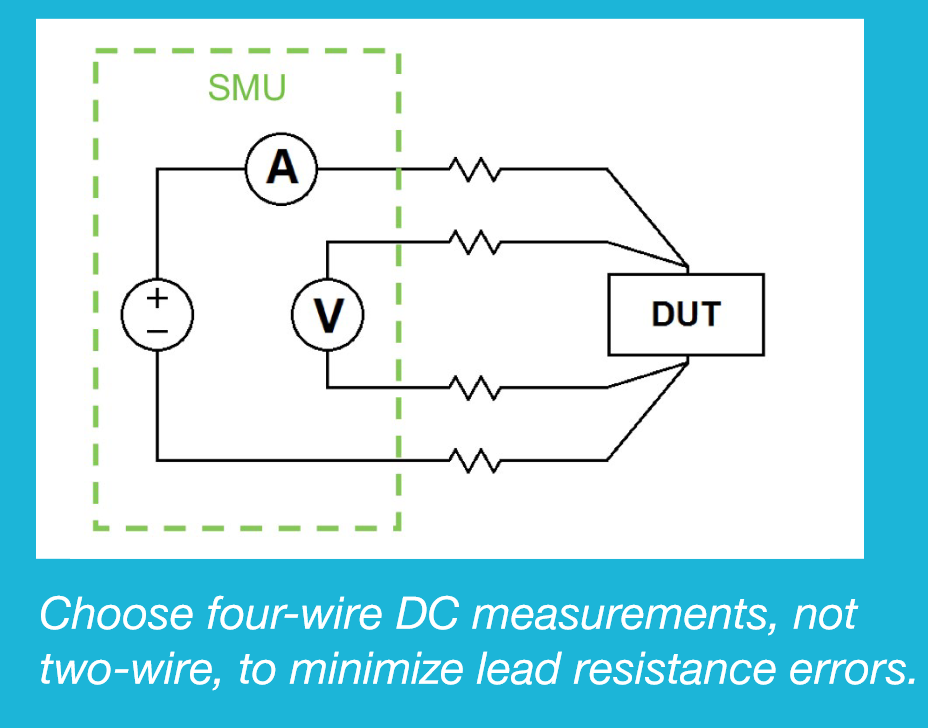
For low resistance measurements, the traditional twowire technique incorporates unwanted lead resistance into the measurement. The test current causes a small but significant voltage drop across the lead resistances, so the voltage measured by the meter isn’t exactly the same as the voltage directly across the test resistance, leading to significant error. With the four-wire (Kelvin) connection method shown here, the test current is forced through the test resistance and through one set of test leads; the voltage across the DUT is measured with a separate set of sense leads. Any small currents that flow through the sense leads are typically negligible, so the voltage measured by the source measure unit (SMU) instrument is essentially the same as the voltage across the resistance. Voltage-sensing leads should be connected as close to the resistor under test as possible.
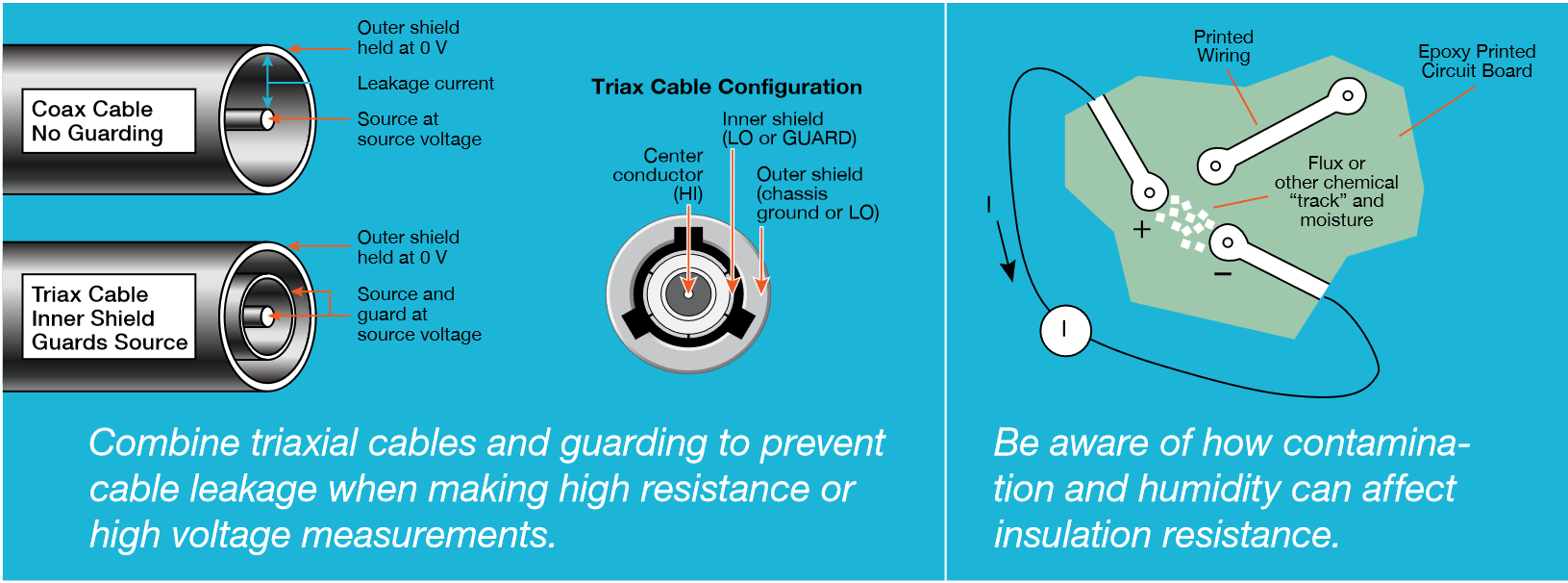
Guarding is often used to prevent current leakage through a cable’s insulation. Connecting a guard voltage to the shield of a coaxial cable can present a safety hazard if the guard voltage exceeds 30 Vrms. Triaxial cabling eliminates this hazard by surrounding the guard shield with an outer shield connected to earth ground or LO. This arrangement provides the capability of safely carrying two signals, neither of which is at ground potential, while maintaining high impedance integrity by shielding both leads and maintaining a high resistance between each conductor and ground. When using an SMU to measure low current, the guard terminal reduces leakage current of the cable and test fixturing.
High humidity (due to condensation or water absorption) and ionic contamination (from body oils, salts, or solder flux) can reduce the insulation resistance of test fixtures dramatically, which can have a serious effect on high impedance measurements. Any moisture can combine with any contaminants present to create electrochemical effects that can produce offset currents. For example, if epoxy printed circuit boards aren’t thoroughly cleaned of etching solution, flux, or other contamination, currents of a few nano-amps can be generated between conductors. To avoid these problems, select insulators that resist water absorption, and keep humidity to moderate levels (ideally <50%). Keep all components and test fixturing in the test system clean and free of contamination.
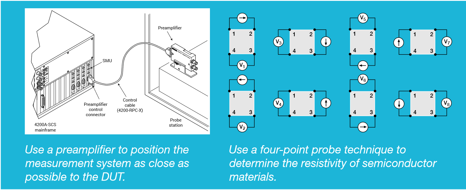
For very low current or very high resistance measurements, even a small amount of noise in the instrument cabling can produce a poor signal-to-noise ratio. Moving the measurement system closer to the DUT is the usual advice for eliminating this kind of noise, but it can be difficult to locate an instrument immediately next to the DUT. However, mounting a preamplifier module close to the DUT on a probe stand or test fixture can make it easy to pull the signals of interest out of the noise floor.
With a four-probe, or Kelvin, technique, two of the probes are used to source current and the other two probes are used to measure voltage. Using four probes eliminates measurement errors due to the probe resistance, the spreading resistance under each probe, and the contact resistance between each metal probe and the semiconductor material. Because a high impedance voltmeter draws little current, the voltage drops across the probe resistance, spreading resistance, and contact resistance are very small.
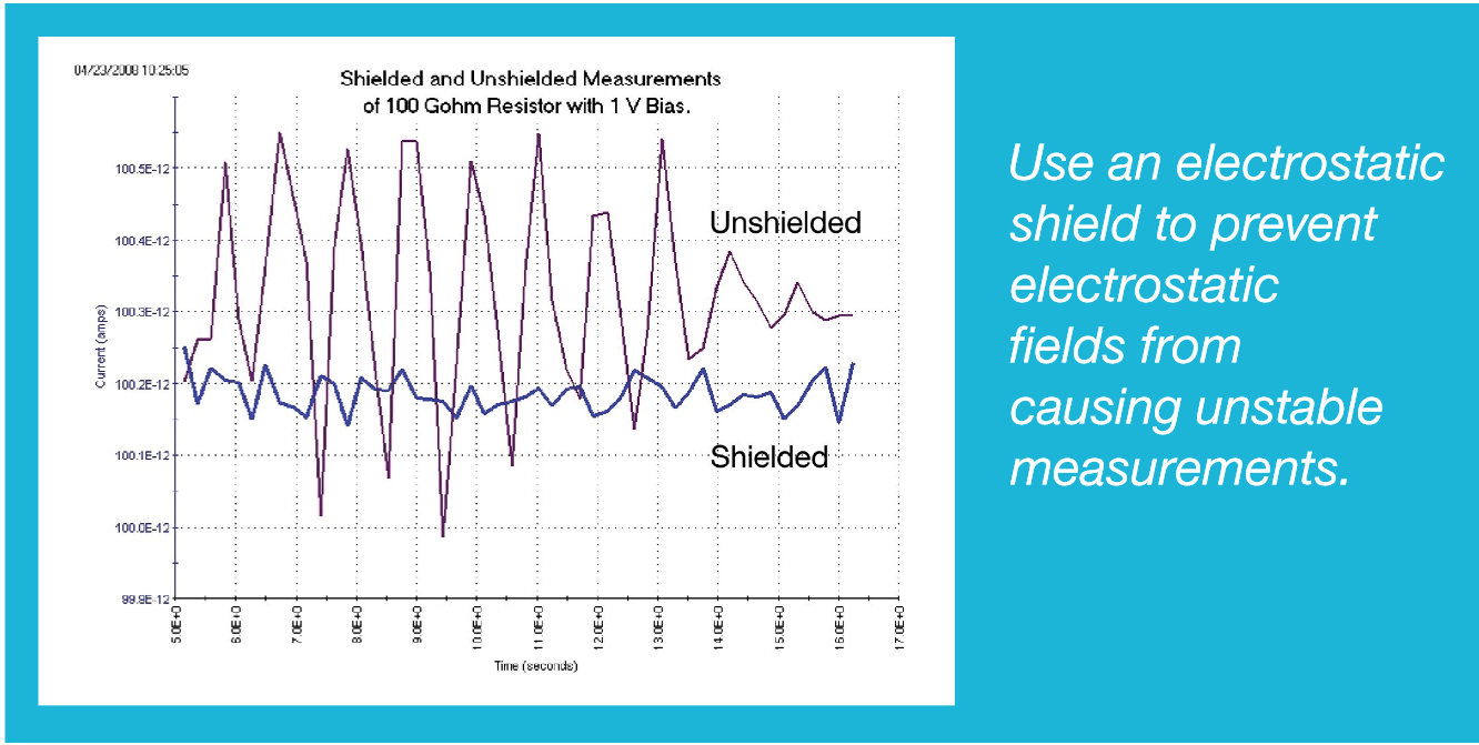
Electrostatic interference occurs when an electrically charged object is brought near an uncharged object. Usually, the effects of the interference are not noticeable because the charge dissipates rapidly at low resistance levels. However, high resistance materials do not allow the charge to decay quickly, and unstable measurements may result. Typically, electrostatic interference is an issue when making current measurements ≤1 nA or resistance measurements ≥1 GΩ. To reduce the effects of the fields, the circuit being measured can be enclosed in an electrostatic shield. Note the dramatic difference shown between an unshielded and a shielded measurement of a 100 GΩ resistor. The unshielded measurements are much noisier than the shielded measurements.
What about my AC impedance measurements? How can I diagnose and correct the errors in those?
A variety of techniques can be useful for tracking down the source of AC impedance measurement problems.
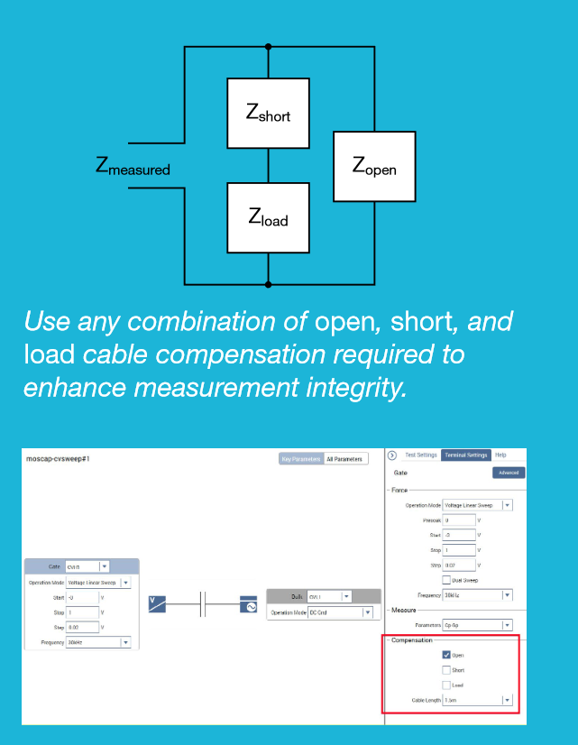
Open compensation, which is performed with the DUT removed, is used mostly to compensate for any capacitance in the cabling or the test fixture. Short compensation, which is performed with a jumper in place of the DUT, is used mostly to compensate for any inductance in the cabling or the test fixture. Load compensation, which requires a load that’s calibrated over the entire frequency range of the meter, is performed with this load in place of the DUT and compensates for any nonlinearity or gain error in the actual measurements.
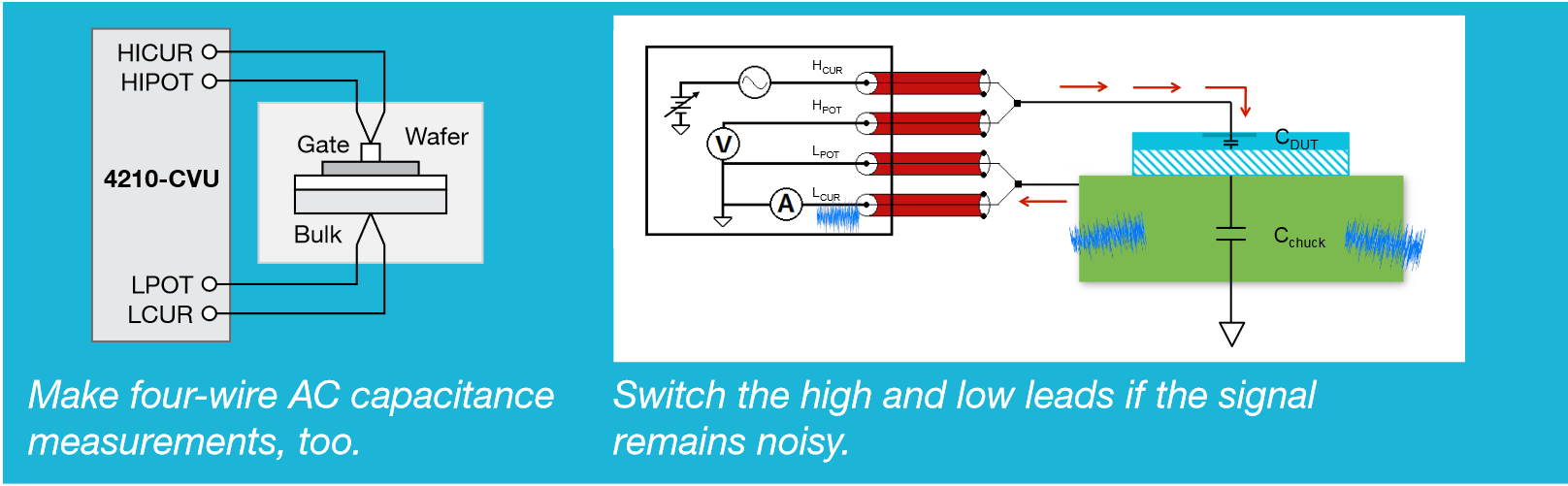
Occasionally, even when using a four-wire configuration and cable compensation, noisy signals can still disrupt crucial measurements. This noise is especially apparent with capacitance measurements because they involve measuring tiny currents that are highly susceptible to noise and because sourcing and measurement are performed on different terminals; a seemingly quiet system can have noise that is simply localized near the measurement terminal. Because of the separation of source and measure, this noise can often be reduced or eliminated by switching the position of the high and low leads, thereby changing the terminal on which the measurement takes place.
A probe station chuck is an extremely large capacitor that can act as a large antenna that collects random noise. Because the substrate is electrically connected to the prober’s noisy ground, the ammeter will be sensitive to this noise and will cause capacitance measurement errors. When making a capacitance measurement, always connect the AC ammeter to the terminal of the device with the least noise, which generally means the least amount of capacitance to ground.
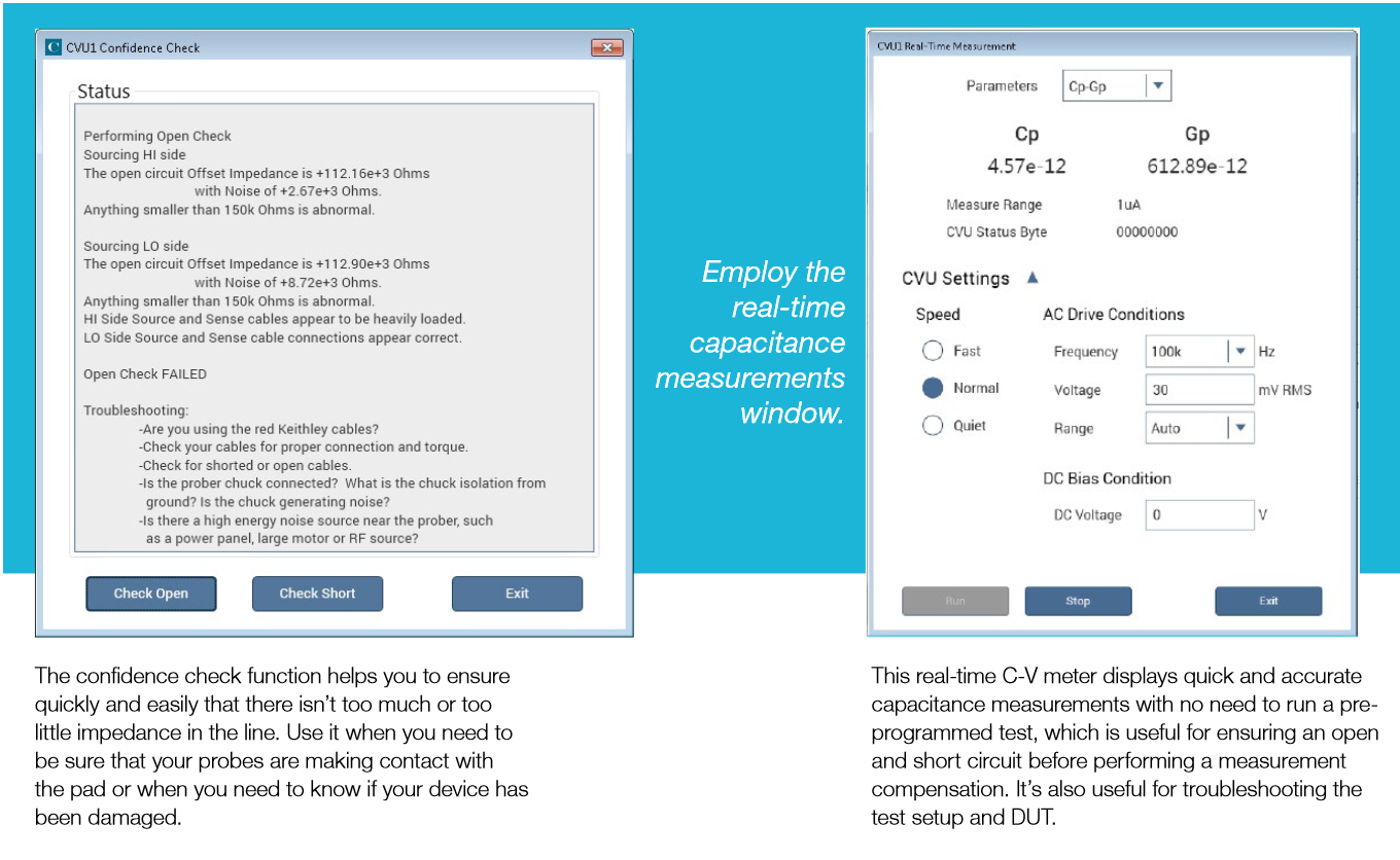
Although finding the least noisy device terminal can be done manually, newer systems provide software that supports switching around the AC source, DC bias, and ammeter locations to find the quietest terminal without having to change cables manually, lift the prober needles, or change the test setup. This ensures the AC signal is being measured on the least noisy terminal.
How can I minimize errors when making DC measurements on MOSFETs and MOScaps?
Follow these best practices for commonly performed DC tests like VDS-ID sweeps, VGS-ID sweeps, and subthreshold voltage sweeps.
The approach shown in the upper configuration allows every node to be held at a feedback-controlled voltage and every current to be measured. But if a separate SMU isn’t available for each channel, connections can be made as shown in the lower configuration. However, this configuration is more susceptible to a noisy ground connection and can produce ground loops if long cables are used. Also, the current and voltage at the source terminal cannot be measured, which can lead to errors in calculations.
The VDS-ID test involves sweeping the drain-source voltage while holding the gate-source voltage constant. This test produces the familiar family of curves associated with MOSFET characterization. To produce the curves shown here, the gate is set up to step from 2 V to 5 V with four 1 V steps. For each gate voltage step, the drain voltage is swept from 0 V to 5 V. These results offer important insights into the properties of the device.
The blue plot line illustrates how a FET can be used as a voltagecontrolled current source. Varying the gate voltage while holding the drain voltage constant produces an important characterization curve. This measurement also allows calculating the threshold voltage graphically by extrapolating a line tangent to the curve and finding its zero-intercept. The red plot line illustrates calculating the transconductance (gm) and finding the maximum transconductance value (Vth).
What are the best practices for making common C-V measurements on MOSFETs and MOScaps?
Many C-V measurements of a FET require tying the drain, source, and bulk terminals together, either by soldering them or by making the appropriate probe station connections. The first step is to connect the CV HI terminals of the C-V meter to the gate of the device and the CV LO terminals to the drain/source/bulk of the device. Then, perform the cable compensation measurements: first, remove the device and perform an open compensation; place a jumper between where the gate and drain/source/bulk terminals would be and perform a short compensation; finally, insert a load in place of the jumper and perform a load compensation. Once the FET is replaced, the setup for making accurate C-V measurements is complete.
The results of a simple C-V sweep can offer a wealth of information on an MOS device. The gate-bulk voltage and gate capacitance measurements can reveal its oxide thickness and impurity concentration. From these values, gate oxide thickness can be calculated using the standard parallel plate capacitor equation and the impurity concentration and Fermi potential can be calculated with further equations.
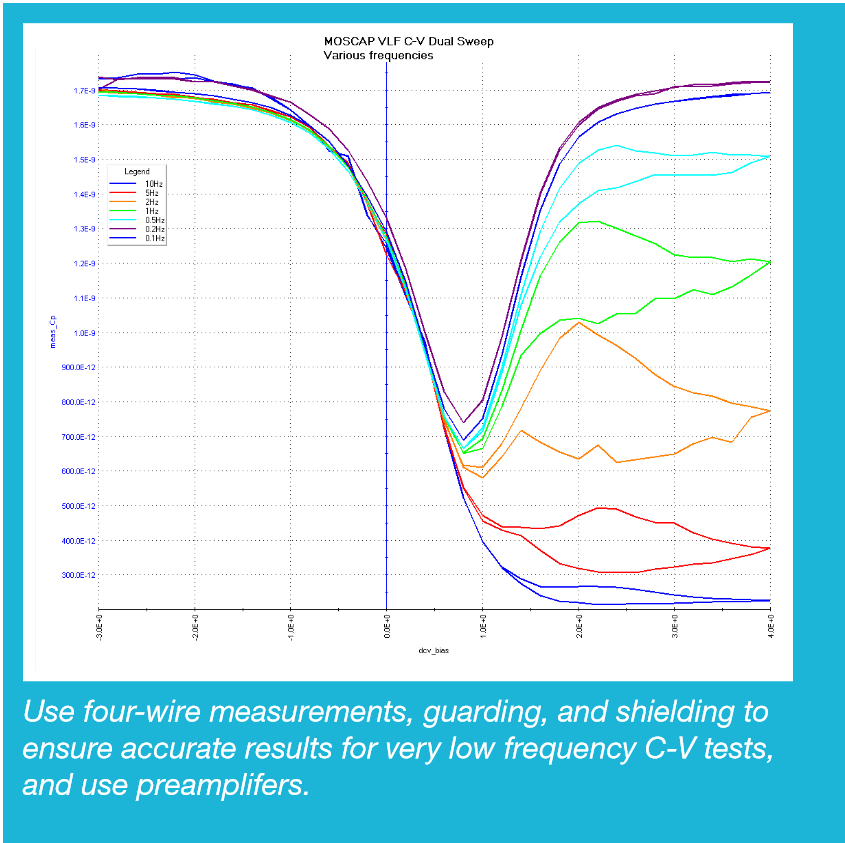
A 10 Hz C-V sweep over a capacitor allows analyzing device characteristics evident only at low frequencies. This test is generally performed on a test MOScap device elsewhere on the wafer. Because the test’s maximum frequency of 10 Hz is well within the performance capabilities of an SMU instrument, it employs SMUs to make ultra-low current measurements.
Whenever I have to reconfigure my probe station to switch from making DC I-V measurements to C-V measurements, I start having measurement problems. Why is this so complicated?
Measurements made at the wafer level using a prober station typically require the use of a patch panel with connectors that do not match the C-V meter, which in turn does not match the DC instruments. These connections require different adapters for each configuration and can be located in hard-to-reach places around the lab. Typically, each time a test configuration requires rewiring the connections, the cable constants change slightly. That makes it necessary to rerun any compensations to update the constants being used, slowing the testing process and increasing the chances of making a mistake. When a previous test must be repeated, it involves repeating all these steps, and it’s never possible to reproduce the constants exactly as before.
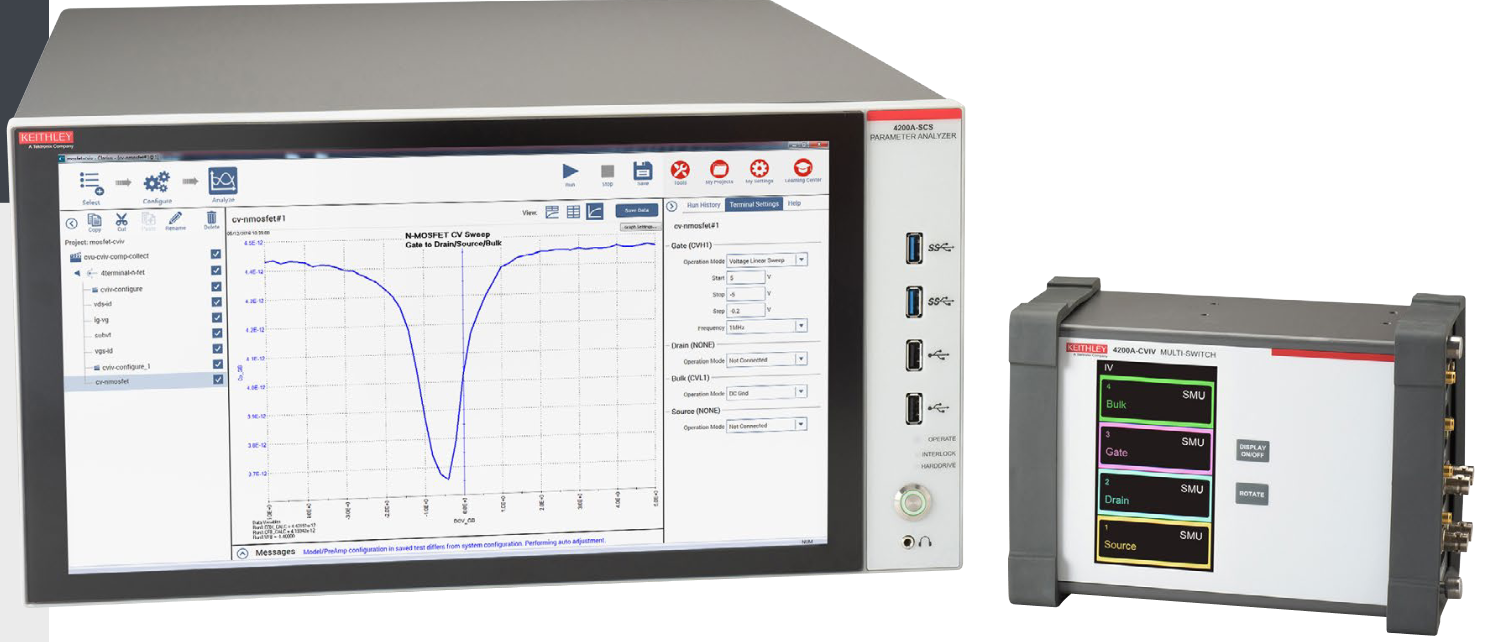
The 4200A-CVIV I-V/C-V Multi-Switch Module can eliminate that hassle and measurement uncertainty. When used with the 4200A-SCS Parameter Analyzer, it automatically switches between I-V and C-V measurements. In addition, C-V measurements can be moved to any output channel without re-cabling. This four-channel switch makes it easy to maintain the same impedance during the I-V and C-V tests by keeping the probe needles on the wafer test site. In addition, the test setup and cables don’t need to be changed to enhance the measurement.
With four output channels, the 4200A-CVIV can switch up to four SMUs on or off independently. It also has three 1×4 multiplexers for the CV HI terminals, the CV LO terminals, and the outer shield of the CVU cables. Each CVU channel can switch to any or multiple output channels. Any channel can be switched open as well, which will leave the output floating. Each of four SMU input channels can support a preamplifier module (for enhanced low-current performance) or a pass-thru module.
So, how do I make connections?
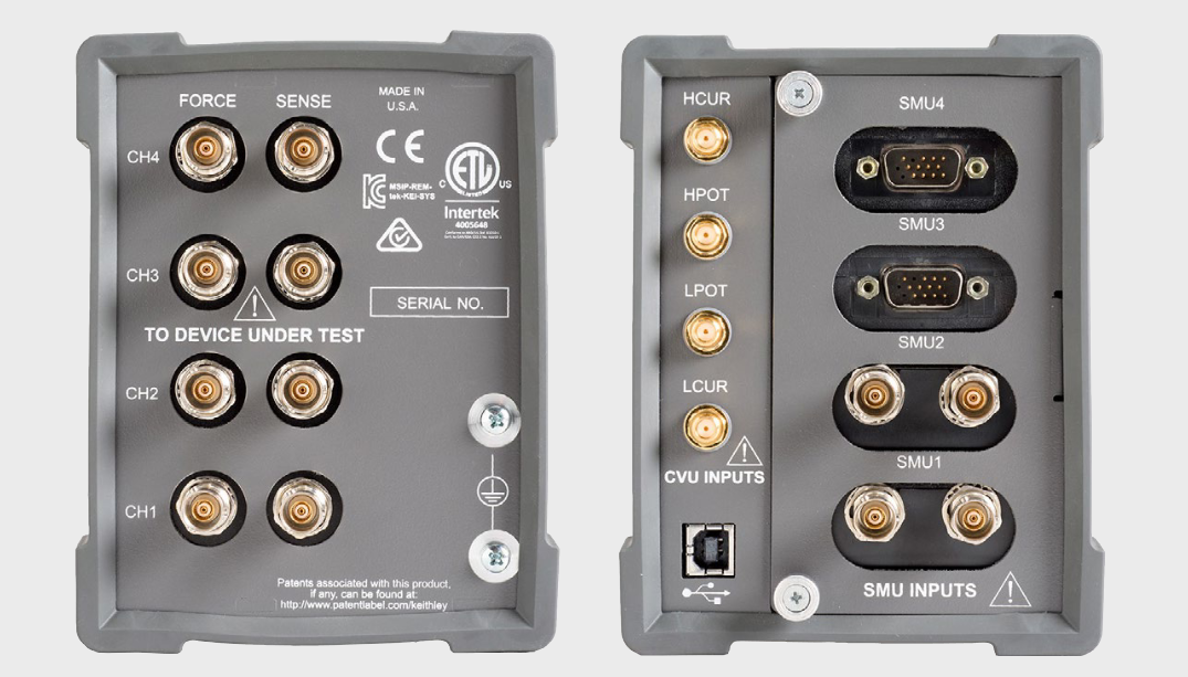
Here are the external connections for the 4200A-CVIV multi-channel switch. C-V measurements can be moved to any output channel without re-cabling. Each channel is user-configurable for low current measurement using the 4200-PA preamplifier or standard current resolution with a SMU Pass-Thru 4200A-CVIV-SPT. The 4200A-CVIV is powered from the 4200A-SCS mainframe via a USB cable.
And, then how do I control this switch?
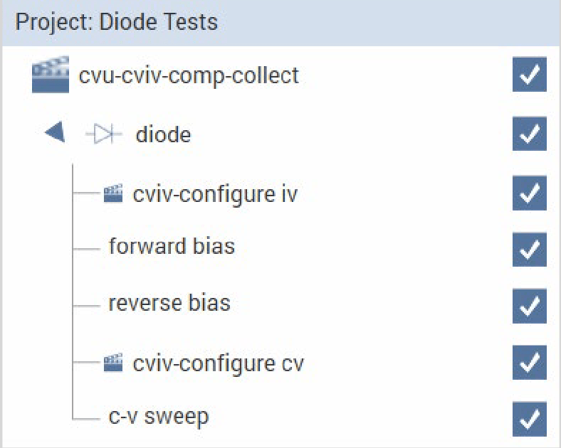
The Clarius ™ GUI-based Software that runs on the 4200A-SCS makes it simple to control the 4200-CVIV Multi-Switch and creates a faster, more efficient device testing workflow for any application that requires making I-V and C-V measurements on the same device. In addition to custom action steps to configure the CVIV switch, Clarius provides cable compensation action steps that are unique to each CVIV configuration. The easyto-use project tree structure like the sequence shown here simplifies setting up the sequence of tests the application demands.
Here’s what you can do with the 4200A-CVIV
- Simply switch between measuring I-V and C-V on the same device
- No need to re-cable
- No need to rerun compensations
- Easily rerun a test with a different configuration
- Measure C-V between multiple sets of terminals on the same device without switching their cables
- Saves time and cabling
- Switch up to four SMUs on or off.
- Multiplex CVHI or CVLO to any combination of four channels
- Open any terminal to leave it floating
- Connect CV Guard Shield to any channel to eliminate noise
My lab has a really limited budget. How can I make all these measurements and follow best practices without spending money I don’t have?
Look for solutions that can be configured in multiple ways to address multiple test needs without compromising performance or accuracy
The 4200A-SCS Parameter Analyzer can be configured with up to nine SMUs. Two SMU models are available: a medium power SMU that has a range up to 210 V/100 mA and a high power SMU that has a range up to 210 V/1 A. Each 4200-SMU medium power SMU or the 4210-SMU high power SMU occupies one slot in the mainframe and can be used together in the 4200A-SCS system. All 4200A-SCS SMUs have shielded triaxial connections with active guarding for low current and high impedance measurements and four-wire (Kelvin) force and sense connections.
The optional 4210-CVU Multi-Frequency C-V Instrument Module for the 4200A-SCS measures AC impedance by applying a DC bias voltage and sourcing an AC voltage across the device under test (DUT) and then measuring the resultant AC current and phase angle. It can make multifrequency capacitance measurements from femtofarads to microfarads at test frequencies from 1 kHz to 10 MHz and while providing a DC bias voltage of up to ±30 V or 60 V differential. With up to 4096 measurement points, it can be used to measure capacitance vs. voltage (C-V), capacitance vs. frequency (C-f) and capacitance vs. time (C-t) to extract many important parameters, including doping profiles, oxide thickness, carrier lifetime, and junction, pin-to-pin, and interconnect capacitance.
The 4200A-CVIV Multi-Switch makes it easy to perform I-V and C-V measurements on the same device without the need to change cables, which could potentially introduce errors or damage devices. The 4200A-SCS and Clarius software make it simple to control the 4200A-CVIV and integrate C-V and I-V testing together into a single project that executes seamlessly and continuously.
When the SMUs installed in the 4200A-SCS are configured with the optional 4200-PA Remote Preamp, they are capable of exceptionally low current measurements. The 4200-PA provides 10 aA resolution by adding additional current ranges to either SMU model. To the user, the SMU simply appears to have additional measurement resolution available. The 4200-PA can be installed on the 4200A-SCS back panel or placed in a remote location (such as in a light-tight enclosure or on the prober platen) to eliminate measurement problems due to long cables.
Where can I learn more about handling my semiconductor characterization challenges?
Consult our growing library of semiconductor characterization resources.
Methods and Techniques for Semiconductor Characterization
Optimizing Low Current Measurements with the 4200A-SCS Parameter Analyzer
van der Pauw and Hall Voltage Measurements with the 4200A-SCS Parameter Analyzer
Resistivity Measurements of Semiconductor Materials Using the 4200A-SCS Parameter Analyzer and a Four-Point Collinear Probe
Techniques For Measuring Resistivity For Materials Characterization
An Ultra-Fast Single Pulse (UFSP) Technique for Channel Effective Mobility Measurement
C‑V Characterization of MOS Capacitors Using the 4200A-SCS Parameter Analyzer
Performing Very Low Frequency Capacitance-Voltage Measurements on High Impedance Devices Using the 4200A-SCS Parameter Analyzer
Using the Ramp Rate Method for Making Quasistatic C-V Measurements with the 4200A-SCS Parameter Analyzer
Using the 4200-CVU-PWR C-V Power Package to Make High Voltage and High Current C-V Measurements with the 4200A-SCS Parameter Analyzer
Switching Between C-V and I-V Measurements Using the 4200A-CVIV Multi-Switch and 4200A-SCS Parameter Analyzer
Make I-V and C-V Measurements 2x Faster 4200a Scs Parameter Analyzer
How to make automatic I-V and C-V measurements
Electrical Characterization of Carbon Nanotube Transitions (CNT FETs) with 4200A-SCS Parameter Analyzer
Electrical Characterization of Photovoltaic Materials and Solar Cells with the 4200A-SCS Parameter Analyzer
4200A-SCS tour
4200A-SCS data sheet
Video: Effortless Parametric Test - 4200 SCS