Introduction
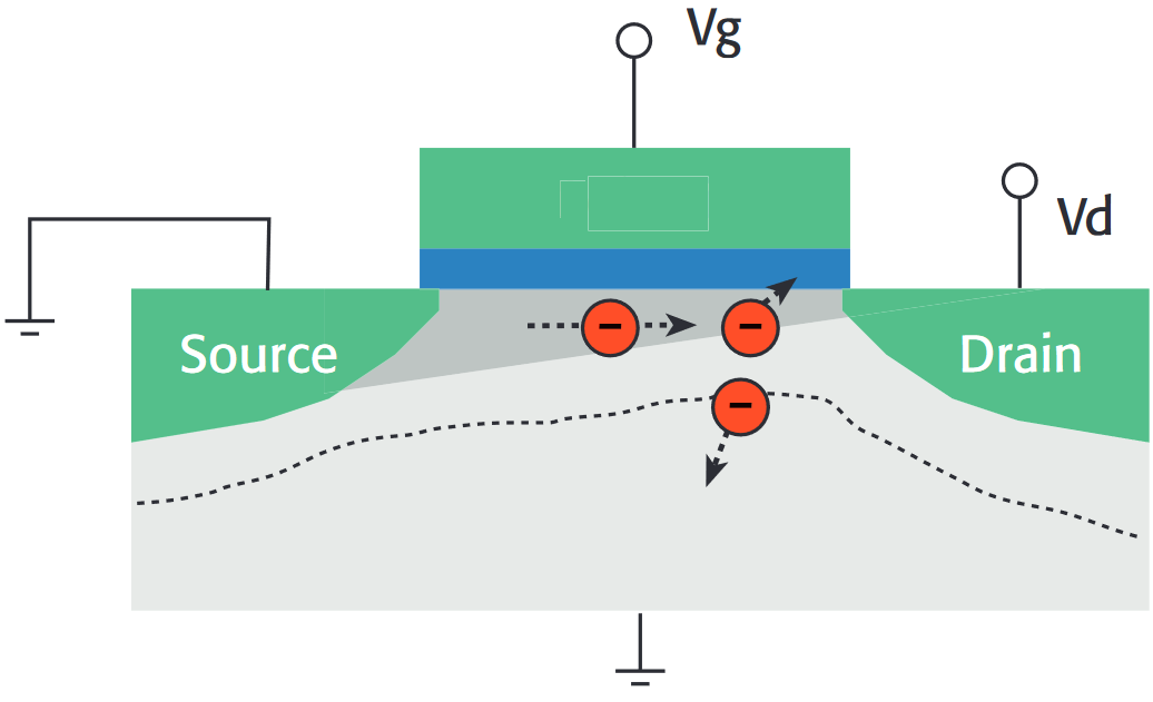
Channel Hot Carrier (CHC) induced degradation is an important reliability concern in modern ULSI circuits. Charge carriers gain kinetic energy as they are accelerated by the large electric field across the channel of a MOSFET. While most carriers reach the drain, hot carriers (those with very high kinetic energy) can generate electron-hole pairs near the drain due to impact ionization from atomic-level collisions. Others can be injected into the gate channel interface, breaking Si-H bonds and increasing interface trap density. The effect of CHC is time dependant degradation of device parameters, such as VT, IDLIN, and IDSAT.
This channel hot carrier induced degradation (also called HCI or hot carrier injection) can be seen on both NMOS and PMOS devices and will affect device parameters in all regions, such as VT, sub-threshold slope, Id-on, Id-off, Ig, etc. The rate of degradation of each parameter over stress time depends on the device layout and process used.
Procedures for CHC Degradation Test
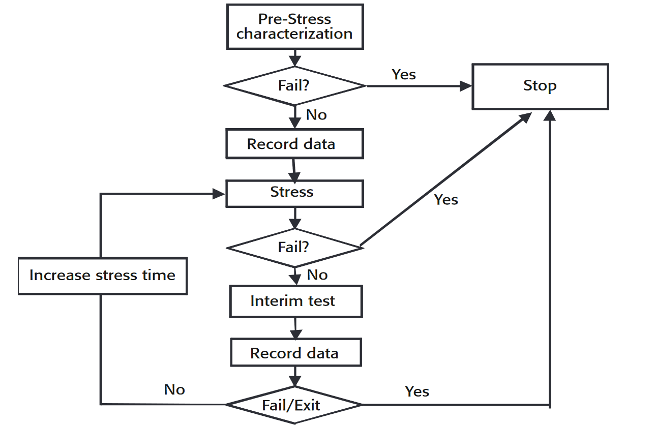
A typical Channel Hot Carrier test procedure consists of a prestress characterization of the device under test (DUT), followed by a stress and measurement loop [1] ( by a stress and measurement loop [1] (Figure 2 Figure 2). In this loop, devices are stressed at voltages higher than normal operating voltages. Device parameters, including IDLIN, IDSAT, VT, Gm, etc, are monitored between stresses and the degradation of those parameters is plotted as a function of accumulated stress time. Prior to conducting this stress and measurement loop, the same set of device parameters is measured to serve as baseline values.
Stress bias conditions are based on worst-case degradation bias conditions, which are different for NMOS and PMOS FETs. Typically, for drain voltage stress, it should be less than 90% of the source drain breakdown voltage. Then, at the drain stress voltage, the gate stress voltage is different depending on the type of transistor and gate length. Table 1 shows worst-case degradation bias conditions for NMOS and PMOS FETs created using different technologies [2].

The worst-case stress bias conditions can be easily determined using interactive test modules (ITMs) on the Model 4200-SCS Semiconductor Characterization System.
Device connections
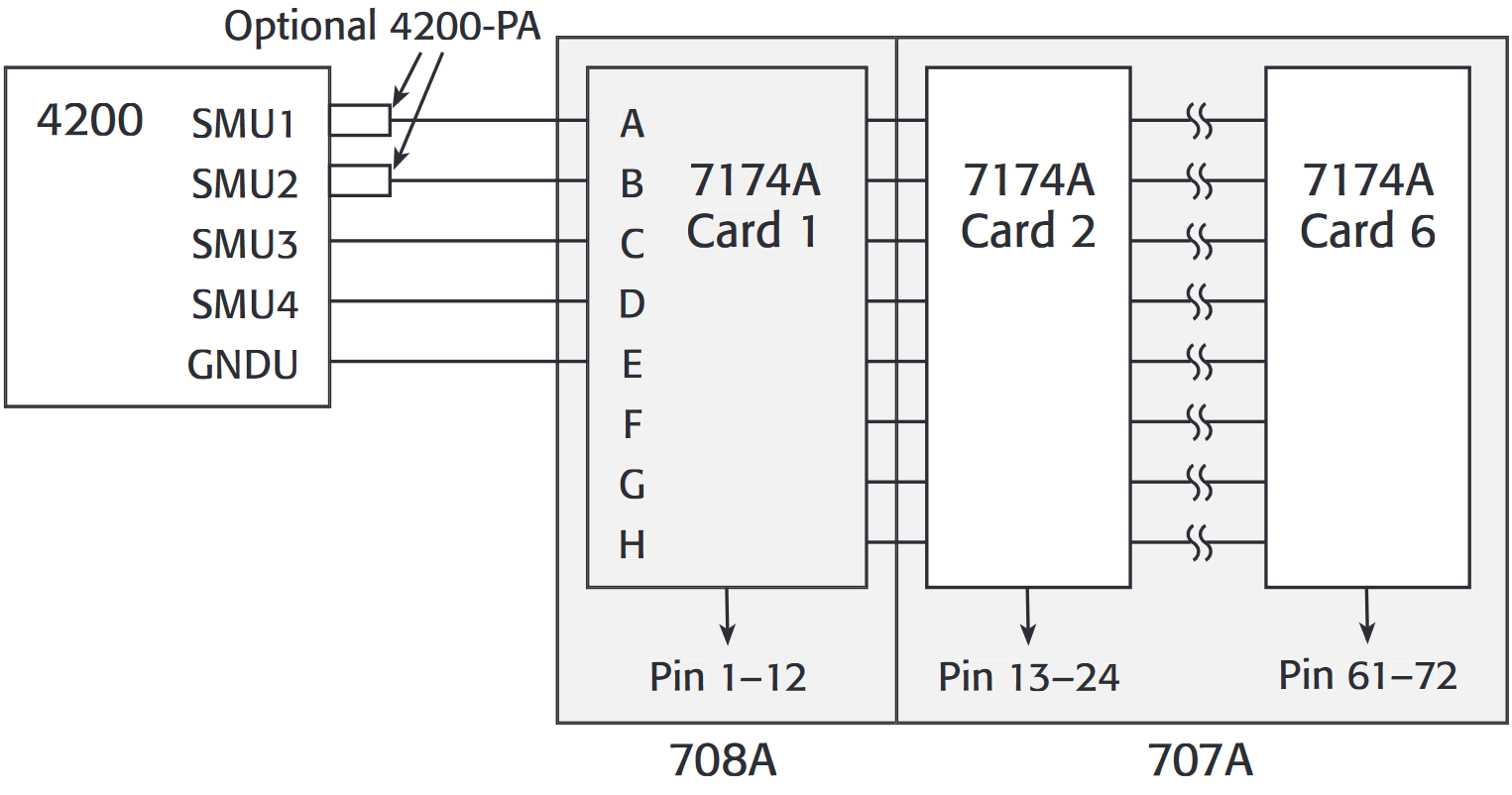
It’s easy to perform a CHC test on a single transistor. However, each CHC test typically takes a long time to complete, so it’s desirable to have many DUTs stressed in parallel, then characterized sequentially between stresses to save time. To accomplish this, a switch matrix is needed to handle the parallel stresses and sequential measurements between stresses. Figure 3 shows an example of a hardware configuration for a typical CHC test for multiple DUTs. The Model 4200-SCS provides the stress voltages and measurement capability, while the switch matrix enables parallel stress and sequential measurements of multiple devices.
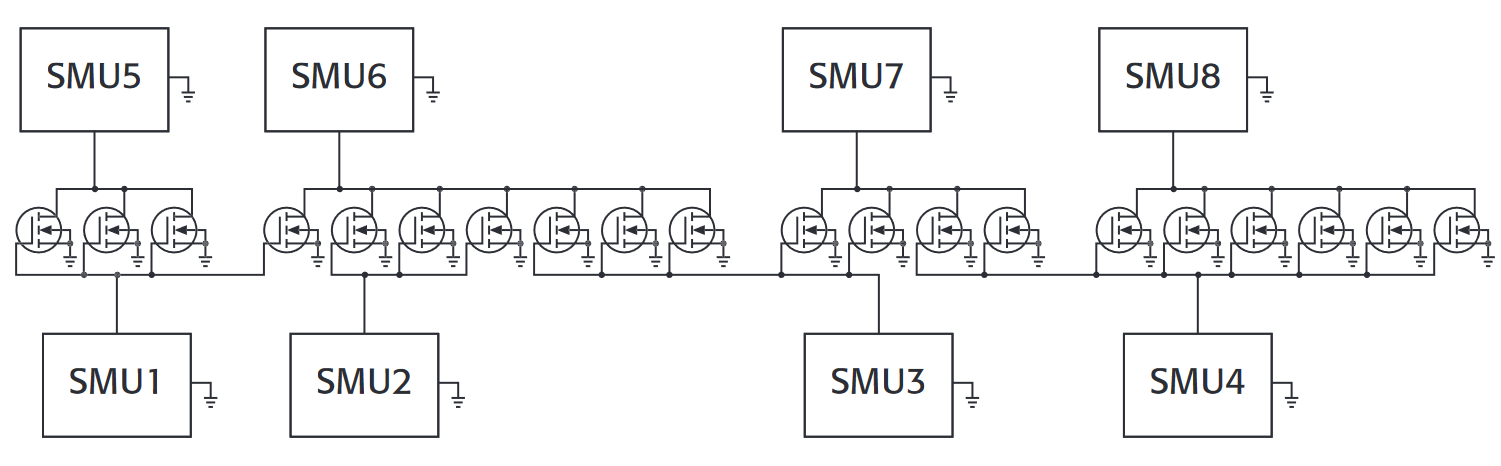
Depending on the number of devices under test, it’s possible to use either the Model 708A mainframe, which accommodates one switch matrix card (12 device pins), or a Model 707A mainframe, with up to six matrix cards (72 pins maximum). The total number of different gate and drain stress biases is limited by the number of SMUs in the system. Figure 4 illustrates a connection diagram using eight SMUs (for total of eight different drain and gate stress biases) plus a ground unit (for ground terminal) to stress 20 transistors in parallel.
Determining device parameters
Hot carrier parameters monitored include VTH, GM, IDLIN and IDSAT. These parameters are initially measured before stress and re-measured at each cumulative stress time. The IDLIN is the measured drain current with the device biased in the linear region, while IDSAT is the measured drain current with the device biased in the saturation region. VTH and GM can be determined using either constant current or extrapolation methods. In the extrapolation method, the VTH is determined from the maximum slope of the IDS vs. VGS curve.
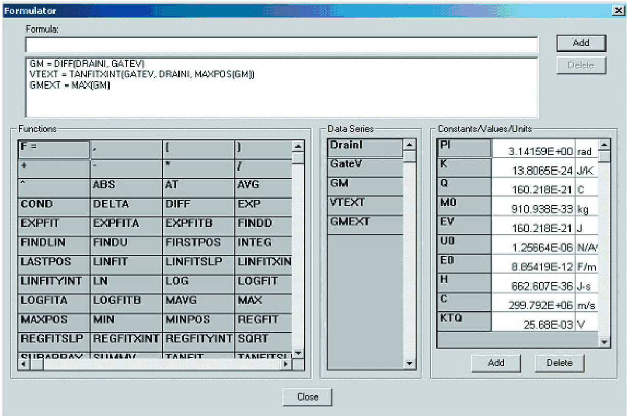
The Model 4200-SCS’s Formulator Tool greatly simplifies extracting these parameters. Built-in functions include Differentiate to obtain GM, a MAX function to obtain the maxi- function to obtain the maximum GM (Gmext), and a least squares line-fit function to extract VTH (Vtext). The formulas to calculate these parameters can be found in the HCI projects supplied with the Model 4200-SCS, and corresponding tests in test libraries. Some examples of these formulas include:
GM = DIFF(DRAINI,GATEV)
GMEXT = MAX(GM)
VTEXT = TANFITXINT(GATEV, DRAINI, MAXPOS(GM))
The last equation (VTEXT) is the x intercept of tangent fit of the ID-VG curve at the maximum GM point. Figure 5 illustrates the Formulator Tool interface.
Once those parameters are calculated from individual tests, they can be exported by checking the check box in “Output Value” option for monitoring the degradation over stress time. For each test, an exit on compliance option can be selected, allowing the system either to skip the device or stop the overall CHC test in case of a device failure. For more details on these options, refer to the complete 4200-SCS Reference Manual.
Setting up stress conditions
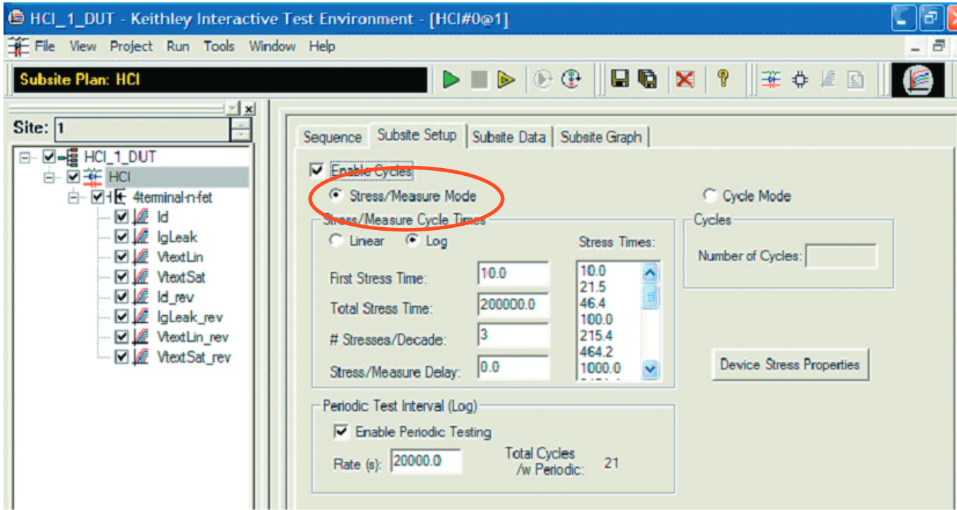
One of the operating features enhanced in version 5.0 of the Keithley Test Environment Interactive (KTEI) software for the Model 4200-SCS software is a stress cycle within the project tree structure with both voltage and current stress capabilities. Users can take advantage of the stress cycle to set up DC stresses on DUTs for preset durations. The duration of the stress for each cycle can be set up in either a linear or a logarithmic way (see Figure 6 Figure 6). This feature is used in CHC/HCI, NBTI, EM (electromi- ). This feature is used in CHC/HCI, NBTI, EM (electromigration) and charge trapping applications to provide a constant DC stress (voltage or current). In stress/measure mode, the user can set up stress conditions for each terminal of the device under test (Figure 7 Figure 7). After each stress cycle, the Model 4200-SCS goes through a measurement sequence, which can include any number and type of user-defined tests and parameter extractions. The degradation of those parameters over time is plotted in the stress graph. The Model 4200-SCS’s “toolkit” architecture offers users tremendous flexibility in creating test sequences and stressmeasure projects.
For critical parameters, a target degradation value can be set (see Figure 7). Once the degradation of that parameter exceeds the target, that specific test will stop. This saves significant time by eliminating unnecessary stress and measure cycles on failed devices.
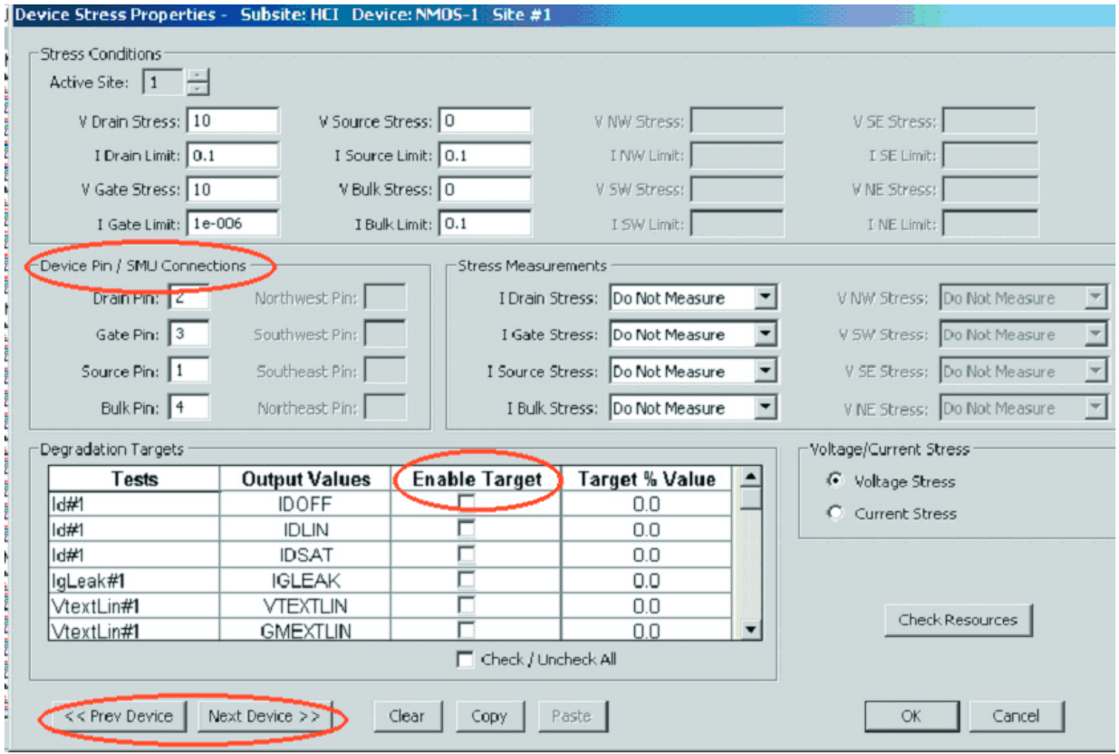
If multiple DUTs are defined in the project, it’s possible to toggle between devices using the “previous device” and “next device” buttons in the device stress set-up window ( device” buttons in the device stress set-up window (Figure 7 Figure 7). The “copy” and “paste” buttons can be used to copy stress settings from one device to the other without the need to re-enter all the information in all the input fields. With multiple devices stressed in parallel in different stress configurations, it can be difficult to correlate the number of different stress biases required and the number of SMUs available to apply them. Pressing the “check resource” button makes it easy to determine if there are enough SMUs for all the stress biases involved, and see how the SMUs are assigned to each of the different stress biases. A ground unit is used by default if the switch matrix is attached to the system and if the stress bias on the terminal is 0V.
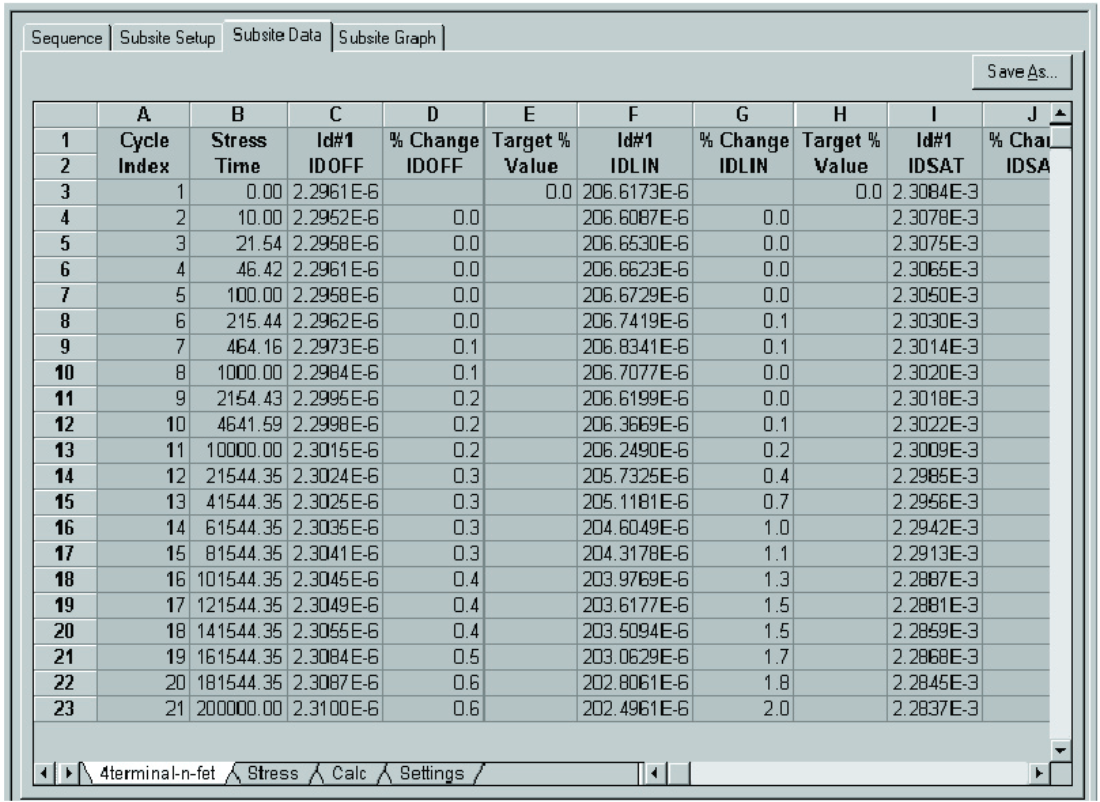
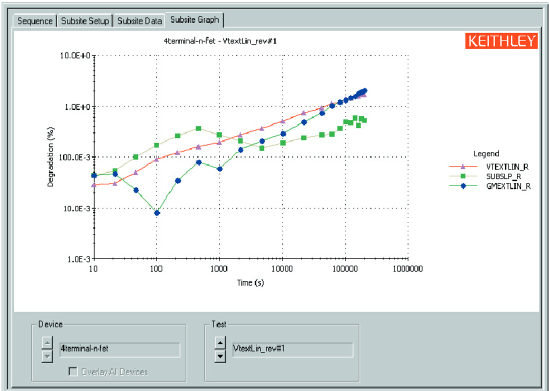
A separate data sheet ( A separate data sheet (Figure 8a Figure 8a) is incorporated within the stress set-up window to save information about cycle index, stress time, and monitored parameters extracted from the measurement between stresses, such as ID and VT. The data is saved automatically in Excel file format (.xls) in the project directory. It’s possible to export the data to other locations as text or Excel files. If the system is in stress/measure mode, the degradation of the monitored parameters relative to pre-stress measurements is calculated automatically and can be plotted on the graph page (Figure 8b Figure 8b). For more information on the stress-measure
Building a CHC project
The following steps outline a typical process for building a CHC project. For details on each step, consult the complete 4200-SCS Reference Manual.
- Create the project structure
- Determine if switch matrix is available
- Determine if enough SMUs are available
- Build project structure
- Build individual tests between stresses
- Make switch connection if switch matrix is used
- Build new test using interactive test modules (ITMs)
- Calculate device parameters using the Formulator tool
- Set up exit on compliance conditions
- Export parameter values for degradation monitoring
- Repeat steps b through e for monitoring more parameters
- Repeat step 2 if there are multiple DUTs
- Set up stress conditions in sub-site level
- Set up stress time
- Set up device stress conditions
- Stress voltage
- Pin connections
- Target degradation values
- Go to next device
- Run project and examine degradation data
Parameter degradation data and raw measurement data are saved automatically in Excel file format during the run time of the project. Therefore, even if the project is stopped before completion, the measured data has already been captured. The raw I-V curves between stresses can be overlaid on stress cycles, so it’s easy to visualize how the I-V degrades as a function of stress time. Figure 9 shows Vgs-Id curves from overlaying 21 stress cycles.
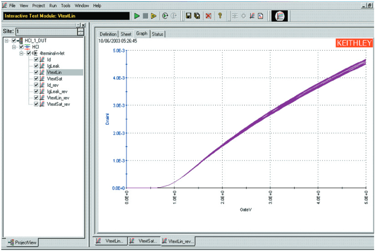
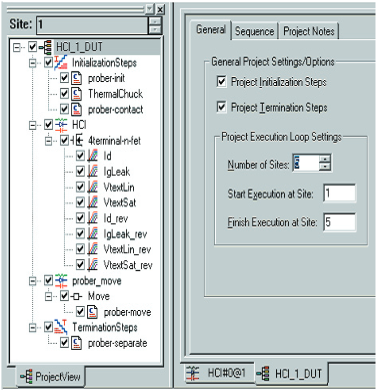
Figure 10 is an example of a CHC project that tests five sites on a wafer. The Model 4200-SCS controls prober movement from site to site through built-in drivers that are compatible with most common semi-automatic probe stations on the market.
Conclusion
The enhanced stress-measure loop in KTEI5.0 software allows setting up a CHC test without the need for any programming. Together with the interactive test interface, Formulator Tool, and powerful graphing capabilities, KTEI 5.0 software makes the Model 4200-SCS an ideal tool for evaluating device reliability parameters such as CHC induced degradation of MOSFETs, as well as its better-known role in device characterization.
References
[1] JEDEC Standard 28-A, “Procedure for Measuring N-Channel MOSFET Hot-Carrier-Induced Degradation Under DC Stress,” 2001.
[2] Vijay Reddy, “An introduction to CMOS semiconductor Reliability,” IRPS Tutorial, 2004.