
- Silicon Carbide and Gallium Nitride demand for 5G, automotive, and energy systems is rising.
- Design complexity is increasing; the time to market window continues to shrink.
- It’s increasingly harder to ensure that designs meet demanding specifications and compliance requirements.
Does this sound all too familiar to you? While we take so much for granted, many engineers and scientists are working everyday with materials like Silicon Carbide (SiC) and Gallium Nitride (GaN) to develop power electronic systems that will drive the new 5G revolution, components and modules for hybrid and electric vehicles, military and aerospace systems, and power systems for computing and consumer products. But what’s the significance of SiC and GaN, and how do you avoid the testing challenges you’re facing with these materials?
After years of research and design, SiC and GaN power devices are becoming more viable. The shift to SiC and GaN is driving new designs from the ground up. SiC, with its capability of driving high power at high voltages for high power applications, and GaN, with its super high-power density for medium to low power applications, are pushing the limits of what is possible with silicon-based designs in efficiency and power density. For example, SiC is finding applications in higher power, higher voltage designs such as motor drives in automobiles, locomotives, and PV inverters. GaN technology is also shaking up the world of RF power amplifiers, thanks to many of the same attributes that make it well-suited for power conversion. GaN is carving its niche in data-center power, wireless power, consumer power supplies, and automotive and military/government power electronics.
These devices, though high performance, come with challenges for designers like you. Setting cost and reliability aside, these power devices are not drop-in replacements for their silicon counterparts. Semiconductor R&D engineers are working to validate and characterize new components. Driver manufacturers are developing new gate drivers to withstand the demands of faster switching, EMI management, and more sophisticated topologies. Manufacturing engineers in these companies are dealing with wafer testing challenges – having to thoroughly test smaller devices over wider voltage and current ranges than ever. Manually characterizing wafer and package-part level devices for electrical performance requires learning new techniques, equipment, and probing infrastructure for low level measurement (e.g., pA of leakage current measurement in the presence of high breakdown voltage).
Some of the biggest challenges working with SiC and GaN devices are the gate drive requirements. SiC requires much higher gate voltage (Vgs) with a negative bias for turn off. GaN, on the other hand, has much lower threshold voltage (Vth), requiring tight gate drive designs. Wide band gap (WBG) devices, by the nature of their physics, also have a higher body diode voltage drop that requires much tighter control of dead-time and turn-on/turn-off transitions.
Solving these challenges may be tough for you. It’s critical that you have accurate electrical source and measure testing when characterizing these high voltage devices so that the right design decisions can be made in a timely fashion. Increasing design margins and overdesigning will only drive costs up and bring performance down. And, due to the high voltages involved - usually >200 V, keeping the scientist and engineer safe from harmful voltage is very important. So, using the right measurement equipment makes all the difference.
Reacting to the challenges we’ve heard from our customers like you, Keithley – a Tektronix Company – has developed the new 2470 High Voltage SourceMeter® Source Measure Unit (SMU) Instrument. The 2470 accurately characterizes most critical DC parameters for optimizing power electronics topologies that use technology like SiC, GaN or any other fast switching silicon power devices.
The 2470 brings 1100 V and 10 fA capability to the engineers’ bench and production floor for product development and DC characterization. Its high voltage and low current measurement performance make the 2470 optimal for characterizing and testing high voltage, low leakage devices, materials, and modules, such as SiC, GaN, power MOSFETs, transient suppression devices, circuit protection devices, power modules, batteries, and much more.


The 2470 features a five-inch, full-color, high resolution touchscreen that supports intuitive operation, helps operators become familiar with the instrument quickly, and optimizes overall speed and productivity. A simple icon-based menu structure reduces the number of steps required to configure a test by as much as 50 percent and eliminates the cumbersome multi-layer menu structures typically used on soft-key instruments.


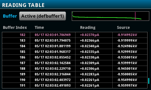
The graphical user interface enables you to convert raw data into useful information without the need for a PC. A full graphical plotting window converts raw data and displays it immediately as useful information, such as semiconductor I-V curves and waveforms. Using the 2470’s sheet view, test data can also be displayed in tabular form. The instrument supports exporting data to a spreadsheet for further analysis, dramatically improving productivity for research, benchtop testing, device qualification, and debugging.
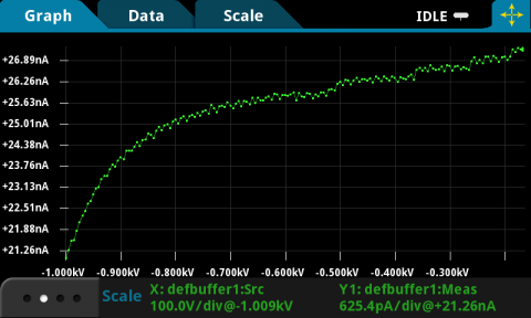
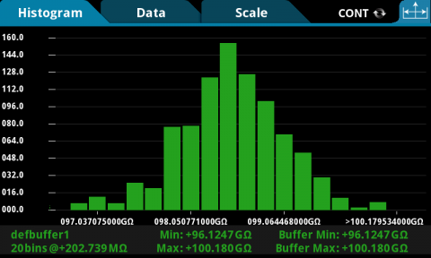
With the 2470’s high voltage and low current measure capabilities, engineers can perform tests on SiC and GaN devices like breakdown and leakage current testing, as well as isolation resistance testing. Measuring breakdown voltage is done by applying an increasing reverse voltage to the device until a certain test current is reached that indicates that the device is in breakdown. In qualifying breakdown voltage, measurements are typically made well beyond the expected rating of the device to ensure that the device is robust and reliable.
In a typical power conversion application, the semiconductor device is used as a switch. Leakage current measurements indicate how closely the semiconductor performs to an ideal switch. Also, when measuring the reliability of the device, leakage current measurements are used to indicate device degradation and to make predictions of device lifetime.
Don’t Forget the Importance of Safety
When testing at high voltage, safety should be of utmost concern to you. The 2470 can source voltage up to 1.1 kV, so be sure to take precautions to avoid exposure to unsafe voltage:
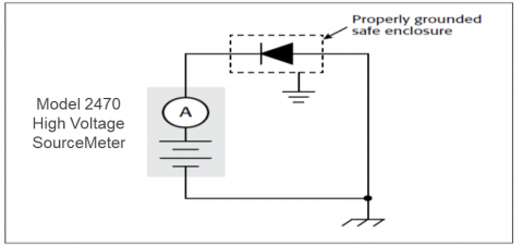
- Enclose the DUT and any exposed connections in a properly grounded fixture.
- Use the safety interlock. The 2470 provides a rear panel safety interlock connection so that the high voltage output is reduced to a safe level if the interlock is not engaged (interlock switch closed.) The interlock circuit of the SMU instrument should be connected to a normally-open switch that closes only when the user access point in the system is closed to ensure that operators cannot meet a high voltage connection to the DUT.
- Use cables and connectors rated to the maximum voltage in the system. Tektronix offers cables that are fully rated for use at 1.1 kV that the test system designer can use to interface to the DUT.
What Big Power Challenges are Your Facing?
Are you equipped for the big power switch to SiC and GaN and ready to overcome the challenges posed by these new materials? I welcome the opportunity to talk with you about your high voltage testing applications and discuss how the new 2470 can help. Please contact me at [email protected] or visit tek.com to learn more.