Introduction
The body of knowledge related to probe cards is far too extensive to cover in a document of this length, so this discussion is limited to issues related to parametric testing. For example, although ceramic ring and blade cards aren't the only types of probe cards available, they are the ones most commonly found in a parametric test environment. This discussion will focus on probe card materials and manufacturing procedures and how these factors affect the signal path, as well as the parameters of concern and the effect of these parameters on test results. Other issues, such as RF testing and probe tip contamination/cleaning, are also addressed.
Probe Card Types
Many different types of probe cards are manufactured, including epoxy, blade, vertical, array, multi-DUT, micro-spring, etc. In this tutorial, the discussion will be limited to epoxy and blade probe cards because they are the types most commonly used for parametric test. These two technologies are very similar in many respects; their key differences typically dictate which one is most appropriate for a specific application.
Each type of card can be characterized by a set of mechanical and electrical parameters. Obtaining reliable test results requires careful matching of these parameters to the type of tester used and the device(s) to be tested. The following discussion addresses how some of these parameters apply to the decision-making process.
Epoxy Ring
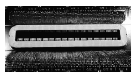
The epoxy ring technology is engineered for applications that require high probe densities and high point counts. Probe counts as high as 2000 aren't uncommon in some custom multi-DUT probe cards. See Figure 1. In the past, blade cards were the primary technology used in parametric test, due to their relatively low cost and suitability for making low-level measurements. However, as the costs for low pin count epoxy cards have fallen and their leakage performance improved, epoxy cards are now often used in parametric testing.
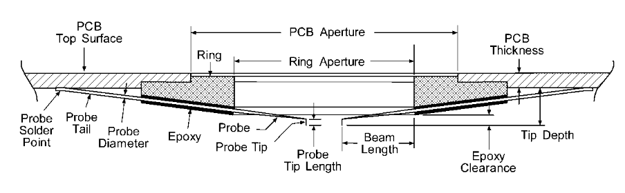
Epoxy ring technology can be extended for low leakage, high frequency, and high temperature applications. The two major components of an epoxy card are the printed circuit board (PCB) and the epoxy ring assembly. Figure 2 is a cross-section of a typical epoxy card PCB with the ring assembly attached.
The ring assembly is built by placing preformed probes into a plastic template. Holes corresponding to the pattern of the bond pads of the circuit to be tested are punched into the template. A ceramic or anodized aluminum ring is epoxied to the probes. The ring and epoxy hold the probes in their proper orientation permanently. The signal frequency of the DUT to be tested typically determines whether a ceramic or aluminum ring is used. Aluminum rings are often used in transmission line probe assemblies for high frequency applications (>2GHz).
After the epoxy has cured, the completed assembly is glued to the PCB, and the probe tails are soldered to appropriate PCB solder points. At this point, user-specified, discrete components capacitors, resistors, etc. can be mounted on the PCB. The final steps in making an epoxy card include probe tip shaping, planarity, final alignment, and QA processes.
Probe card design parameters will vary, based on the IC fab's requirements for device size and shape, number of bond pads, signal characteristics, etc. The probe material used will depend on the test signal characteristics, contact resistance requirements, current carrying requirements, and bond pad material. The probe diameter and beam length are determined by the contact force requirements and current carrying requirements. PCB, tip depth, and epoxy clearance depend on the type of prober interface used. PCB, ring aperture size, and ring aperture shape are determined by the number of probes required and the size and shape of the device(s) being tested. The selection of PCB and ring material depends on probing temperature requirements.
Blade Cards
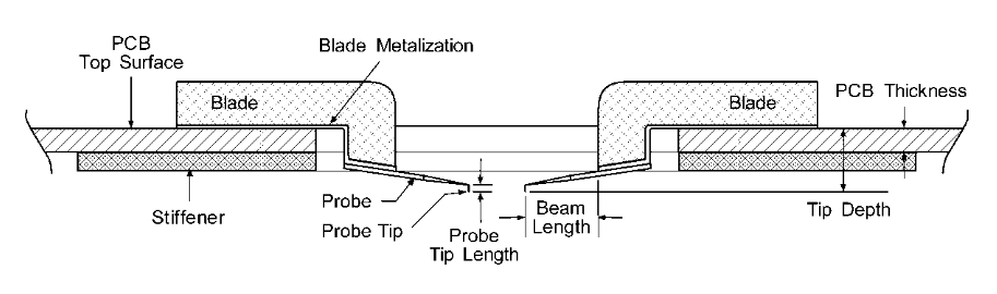
Blade card technology is engineered for applications that require low to moderate probe densities and low to moderate point counts (typically fewer than 80 probes). The technology can be extended for low leakage, high frequency, and high temperature applications.Figure 3 shows a cross-section of a blade card PCB with blades attached.
Unlike ceramic ring epoxy cards, a blade card has no ring assembly. Rather, each probe is mounted on a separate blade, typically a thin, L-shaped piece of ceramic. These "blade probes" are individually soldered on to lands special wide metalized patterns on the top of the PCB.
The most commonly seen blade card (and the only one compatible with Keithley S600 Series testers) is the low leakage card shown in Figure 4. However, as Figure 5 illustrates, many different types and styles of ceramic blade cards are available.
The blade card building process starts with preparing the blade probes. Raw blades are metalized along the bottom edge, as shown in Figure 3. The probes are cut to the proper length and brazed or soldered depending on probe material onto the blades. Finally, the probe tips are bent to the proper angle, making sure that beam length and tip length are in accordance with the specifications.
The assembled blade probes are soldered on to the PCB, along with any user-specified discrete components, such as capacitors, resistors, etc. As with epoxy cards, the final manufacturing steps include probe tip shaping, planarity, final alignment, and QA processes.
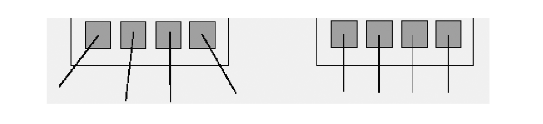
Blade card design parameters are similar to those for epoxy cards, with the exception of the blade. There are three main blade types and the most appropriate one for a specific application will depend on test signal characteristics. A fourth type of blade is used as an edge sensor this is a special configuration with two probes. Edge sensors are used to detect probe touchdown and help set Z height. However, due to improved prober technology, edge sensors are no longer as common as they once were. See Figure 6.
Ceramic blade probes offer superior mechanical stability and a high integrity signal path. With normal usage, ceramic blade probe cards rarely need re-planarization or alignment.
The three most common types are the standard blade, microstrip blade, and the radial microstrip blade. See Figure 7.
Standard ceramic blade probes are used in applications that don't require a controlled impedance environment. Radial microstrip blades are designed for applications that require a controlled impedance environment, where the signal path connects directly to the PCB. Microstrip blade probes are meant for applications that require a controlled impedance environment, where the signal path connects directly to coaxial cable or other types of transmission line. Microstrip and radial microstrip ceramic blade probes are well suited for high speed probing applications. The controlled impedance environment of probe cards built with these probe styles will support test speeds greater than 3GHz.
Ceramic blade and the cantilever wire probe characteristics can be manipulated to optimize the performance of the probe for a given application or operating environment. The ceramic blade parameters with the greatest effect on performance are the blade thickness, shank width, and shank depth. See Figure 8. Increasing the thickness of the blade increases stability. Blade thickness is governed by the number of probes in the array and their proximity to each other. Varying the width of the blade shank increases or decreases the surface area where the blade is attached to the probe. This affects the flexibility of the wire probe and the contact force the probe introduces to the wafer bond pads.
The third variable parameter of the blade is the shank depth. Increasing the depth of the shank increases the distance between the probe card PCB and the wafer under test, which is especially important when testing in a hot chuck environment.
The cantilevered wire probe variations include materials and physical characteristics. Wire diameter, beam length, and material are the primary factors influencing probe contact force and, consequently, scrub length. The probe wire diameter is directly proportional to contact force. Beam length also influences contact force, but the relationship is inversely proportional, so increasing the beam length decreases contact force. The probe tip length and tip angle have a direct effect on scrub length. Longer probe tips are also used on high density probe cards, alternating with standard length tips to ensure proper clearance and signal isolation. The final parameter, probe tip diameter, must be selected to provide good contact force, yet ensure the entire scrub length fits well within the passivation opening.
Epoxy vs. Blade Comparison
Before attempting to determine which card type is needed, the technical requirements of the probe technology must be clearly defined. If a Keithley S600 Series tester is being used, the choice of probe cards is fairly limited. However, it's still possible to specify either an epoxy card or a ceramic blade card.
Typical Technical Requirements
- DC Electrical: Contact resistance, leakage, signal path resistance, probe current capacity, etc.
- AC Electrical: Bandwidth, capacitance, crosstalk, rise times, etc.
- Mechanical: Alignment, planarity, contact force, pad size, pad pitch, layout, etc.
- Other: Environment (temperature), pad damage, lifetime (number of touchdowns), cost, etc.
Use one of the microstrip blade cards if the bandwidth is greater than 3GHz or the leakage specification is less than 1pA/V and there are fewer than 80 pins (68 pins for an S600 Series tester). To use a standard blade card, the pad pitch must be greater than 120 microns and the number of pins must be less than 80 and the pads must be symmetrically placed. The standard epoxy card can be used for all other applications with a frequency less than 2GHz. For an epoxy card used at frequencies higher than 2GHz, use the transmission line probe assembly (aluminum ring).
Remember that the values given here are very loose standards. Anything outside these standards is possible, but requires custom work and engineering support from the probe card vendor. A card's cost depends on many factors and is generally not a differentiator between the two technology types. See Table 1.
| Epoxy Ring | Ceramic Blade | |
| AC Electrical | ||
| Bandwidth >2GHz | Needs work | Very good |
| Crosstalk | PCB layout dependent | PCB layout dependent |
| DC Electrical | ||
| Inductance < 5nH | Needs work | Good |
| Leakage | OK | Very good |
| Signal Path Resistance | PCB layout dependent | PCB layout dependent |
| Mechanical | ||
| Planarity Compliance | Very good | Very good |
| Alignment Compliance | Very good | Very good |
| Min. Pad Pitch | 50mm | 100mm |
| Probe Density | > 2000 probes | < 88 probes |
| Scrub Aluminum Pad | Good | Good |
| Contact Force | Good | Good |
| Other | ||
| Temperature | OK, requires custom >100°C | Best |
| Touchdowns >250k | Very good | Good |
| Customer Repairability | OK | Better |
| Cost of Ownership | Good | Slightly better |
| Addition of Passives | OK | Very good |
Table 1. Epoxy vs. blade comparison.
Bond Pads
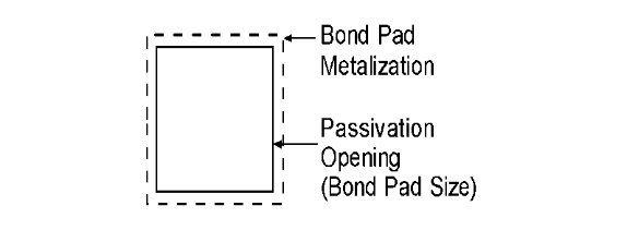
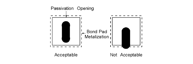
Bond pads are the metalized locations on an integrated circuit where the test probes will make contact. They are typically identified or specified by the X, Y coordinates of their geometric centers. There are two prevailing definitions of bond pad size. One definition is that the bond pad size is equivalent to the size of the passivation opening. The other definition is that bond pad size is equivalent to the metalization size. See Figure 9. Most people in the probe business use the passivation definition. The passivation layer overlaps the edges of the bond pad metalization, so the usable area is often 10% smaller than the metalization in both dimensions.
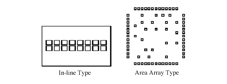
The size, spacing, and configuration of bond pads on a die can have a significant impact on the design and manufacture of epoxy and blade probe cards used for wafer testing. There are many different bond pad configurations from simple in-line designs to complicated area arrays. See Figure 10. It gets far more complicated when dealing with multi-DUT probe cards. In the parametric world, we will normally only be dealing with the simple in-line, single DUT variety
Keithley recommends following some simple guidelines that can help minimize the impact of bond pad layout on probe card design. These are generic guidelines for the standard card. Deviating from these standards is acceptable, but will require engineering input from the probe card vendor.
Pad Size
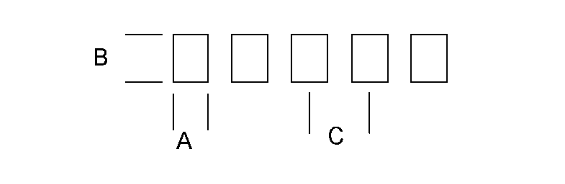
Using the passivation opening: pad size (Figure 11) is generally stated in terms of pad width (A) and pad depth (B). Pads needn't be square. It's preferable to have a greater depth than width.
Pad Pitch
Pitch (C) is the distance between adjacent bond pad centers (Figure 11). When bond pads aren't equally spaced, pad pitch is defined as the smallest spacing between any two adjacent pad centers.
Obviously, a single probe won't work if the bond pad is too small. However, on a multi-probe card, pad pitch is the primary variable that affects probe card design. Pad pitch is, in turn, affected by the device size and number of I/Os. This is generally not a concern in parametric test.
Pad pitches larger than 3.5 mils (89µm) provide the most feasible scenario for probe card design. In this range, the probe card designer has the best opportunity to optimize the design for robustness and manufacturing feasibility. Pad width and depth should fall into the range of 2.5 mils to 3.0 mils (64–76µm) to minimize alignment issues during manufacturing and use. There is no significant advantage to a pad size larger than 3.0 mils (76µm).
Generally, as pad pitch decreases, probe density increases. In either case, it's important to maintain adequate pad width and depth to accommodate the scrub mark. With a pad pitch in the range from 2.5 mils (64µm) to 3.5 mils (89µm), the optimum pad width is also dependent on the diameter of the probe tip being used. As a rule, maintain the pad width at 75% of the pad pitch, but never less than twice the probe tip diameter. For instance, at a pitch of 2.75 mils (70µm), use a pad width of 2.0 mils (51µm) for a 1.0 mil (25µm) tip diameter. Pad depth should be kept at a minimum of 2.5 mils (64µm) to allow for adequate scrub length without interfering with the passivation layer
Except in special cases, a pad pitch of less than 2.5 mils (64µm) is too tight to accommodate in a single row pad configuration and still maintain robust probe geometry for probe card life. In these instances, use two rows of staggered bond pads to provide an "effective" pitch of up to twice the actual pitch. In this scenario, bond pad width can be maintained at 2.5 to 3.0 mils (64–76µm) without impacting pad spacing. See Figure 12.

Table 2 summarizes the bond pad guidelines.
| Pad Pitch | Configuration | Pad Width | Pad Depth |
| >3.5 mils (90µm) | In-line | 2.5-–3.0 mils(64–76µm) | 2.5–3.0 mils(64–76µm) |
| 2.5–3.5 mils(64–76µm) | In-line | 75% of pad pitch or twice the tip diameter (whichever is greater) | 2.5–3.0 mils(64–76µm) |
| <2.5 mils(64µm) | Staggered | 2.5–3.0 mils(64–76µm) | 2.5–3.0 mils(64–76µm) |
Table 2. Single DUT bond pad guidelines
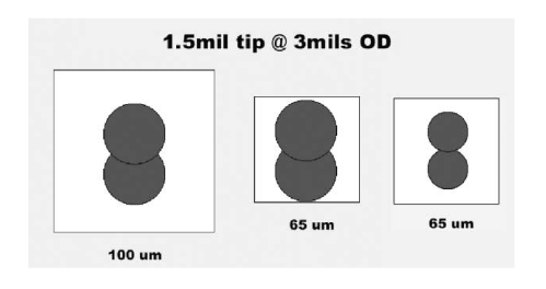
Lately, there has been an effort to reduce bond pad size to as small as 1.8 mils (45µm). For a number of years, the standard probe tip diameter was 1.5 mils and an overdrive of 3 mils. This worked well when the bond pad was 3.9 mils (100µm) because it produced a nice, clean scrub mark. However, when the industry standard for bond pad size shrank to 2.5 mils (65µm), the 1.5 mil tip probe obviously would no longer work. See Figure 13. The probe tip was reduced to 1.0 mil, which initially looked like it would do the trick.
So what was the problem? Conventional alignment and planarity specifications, coupled with existing manual alignment capabilities, are currently limited to 0.0002–0.00025 inches or five to seven microns from true position. And that, without a perfect alignment, put the scrub mark into the passivation. The tip diameter was reduced again, to 0.7 mils, which is now a fairly common diameter. The industry is going through another bond pad shrink. The goal is 1.8 mils (45µm) and the tip size can't be reduced. How is the industry attempting to deal with this issue?
Approach #1: Through layout design of the probe card, angle the probe and scrub mark relative to the bond pad. See Figure 14. The idea is to make use of more of the bond pad for the scrub mark.
Approach #2: Tighten up the planarity and alignment specs. Reduce the overdrive to shorten the scrub mark. See Figure 15. Increase gram force by a factor of two by shortening beam length to compensate for the loss of force due to the reduction in overdrive.
Each of these approaches comes with various problems:
- Auto-probe align.It has been difficult for the prober equipment to deal with the angled scrub approach.
- Continuity issues. An increase in probe force and lack of sufficient scrub has led to an early buildup of non-conductive pad oxides, creating resistance and continuity problems.
- Contamination. The higher gram force required for reduced scrub length has the effect of shaving the bond pad, which leads to aluminum flaking.
These and other challenges are being addressed and 45mm pads are still fairly uncommon.
PCB Materials and Design
Probe card PCB designs can be as simple as a PCB with traces on top and bottom or as complex as a PCB with more than 32 signal layers. In terms of signal layers and layout, parametric probe cards are relatively simple. However, designing probe card PCBs has a unique set of challenges. Most PCB design and the software that supports it are based on a grid system with trace routing primarily in the horizontal and vertical directions. Almost all probe card designs are circular. The design software that normally does the autorouting, design rule checking, GERBER file generation, and net list generation doesn't support circular layouts. For probe cards, these functions must be done by hand. This is true throughout the ATE world and is slowly changing. Many of the software design companies are now beginning to take an interest in circular ATE PCB layout.
Many types of materials can be used in the PCB fabrication process, but the two most often seen in the parametric world are FR4 and polyimide. FR4 is the most common and the less expensive of the two.
FR4
FR4 epoxy glass PCBs are used in most applications where the probing temperatures are less than 100°C. See Table 3 for specs.
| Dielectric constant (1MHz) | 4.5 to 5.0 |
| Dielectric loss (1MHz) | 0.02 to 0.03 |
| Temperature range | 0–100°C |
| Trace-to-trace resistance | >100MΩ or <100nA @ 5V |
| Trace-to-trace capacitance | <5.0pF |
| Leakage current | 2nA/V |
Table 3. Typical spec values for FR4.
Polyimide
Polyimide PCBs are used where high operating temperatures (100°C to 185°C) are involved. Transmission line probe assembly is generally incompatible with high temperature probing and wouldn't be used with a polyimide PCB. See Table 4 for specs.
| Dielectric constant (1MHz) | 3.7 to 3.9 |
| Dielectric loss (1MHz) | 0.0015 to 0.0025 |
| Temperature range | –100°C to 200°C |
| Trace-to-trace resistance | >100MΩ or <100nA @ 5V |
| Trace-to-trace capacitance | <5.0pF |
| Leakage current | 2nA/V |
Table 4. Typical spec values for polyimide.
Layout and Design Guidelines
Here are a few of the more important probe card design guidelines. These guidelines are normally driven by the requirements of PCB fabrication and may vary, depending on the fabrication house used.
- Minimum metal-to-metal spacing should be no less than 0.005 inches.
- No metal should be placed within 0.050 inches of a routed edge or non-plated thru hole edge.
- Minimum trace width of external traces of 0.010 inches.
- Minimum trace width of internal traces of 0.006 inches.
- Signal layers may be internal or external to a multi-layer PCB.
- Pads should be 0.025 inches greater in diameter than the drill holes associated with them (standard) ±0.003 inches tolerance.
Low Leakage PCB Design
This section offers a few tips related to good PCB layout techniques. Low Level Measurements, a Keithley handbook, is another good source of information on low level measurements and leakage path issues.
Fabrication materials, layout, and handling can all directly affect the leakage performance of a probe card. There are a number of common leakage mechanisms:
- On the top and bottom of the PCB, the most common type of leakage occurs between adjacent features, such as traces, conductors, vias, and (sometimes) surface planes. This leakage path can be formed by organic contaminants, PCB reinforcement materials, and solder mask.
- Leakage can occur between layers and be carried by the reinforcement materials.
- Leakage can occur between inner-layer features and be carried through the reinforcement material and the epoxy holding the reinforcement layers together.
Layout Tips
- For systems that are less than 20V, use 1mm or greater separation for surface features.
- Keep leakage-sensitive signals on the top or bottom surfaces.
- Grounded traces between signal traces may reduce crosstalk but may increase leakage.
- Use guard traces for sensitive signals.
- Layer-to-layer leakage is negligible, except for large geometry and ultra-sensitive signal traces.
- For inner-layer sensitive signals (avoid when possible), use the maximum possible separation between the signal and other inner-layer features.
- Three types of solder mask are available: liquid photo-imagable (LPI), wet screenable, and dry film. A bare board is generally best, but if solder mask must be used, don't cover sensitive signal traces. In terms of leakage performance, of the three types of solder mask, LPI is best and dry film is the worst.
- Organic contaminants such as solder flux and body oils are death to low leakage probe cards. Keep the cards clean!
- Generally, bare polyimide has slightly better leakage characteristics than FR4, but is usually not worth the added cost.
Keep in mind that the resistance of a dielectric isn't necessarily linear and that physical characteristics such as feature dimensions and volume resistivities have natural, manufacturer, and lot-dependent variations that will affect the probe card's overall performance.
Impedance Control
Most probe card PCBs are designed for controlled impedance of the signal connected to the testhead interface. Typical impedance matching is 50, 75, and 90 ohms. This is easily incorporated into the design by keeping signal widths constant. Common impedance formulas are fairly complex for both static and dynamic signal paths. Dynamic signals significantly raise the complexity levels; however, in parametric testing, static signals are more common.
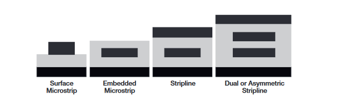
There are four predominant layout methods (Figure 16) for controlling impedance: surface microstrip, embedded microstrip, stripline, and dual or asymmetric stripline. Unless requested by the IC fab, power planes generally aren't used to control impedance. A preliminary dielectric thickness is calculated for the desired impedance and specified on the fabrication drawing, along with the trace width used for the calculation. The vendor who manufactures the PCB may vary the dielectric thickness and the trace width (up to 10% of the designed width) to achieve the specified impedance within the tolerance (usually 10%) specified on the fabrication drawing.
Probe Materials
There are four common types of probe material: tungsten, tungsten-rhenium, beryllium-copper, and Paliney‚7. Refer to Table 5 for their material properties. There are also many other uncommon types, such as silver-plated, insulated, and exotic metal alloys. Each of the four common types of probe material has its own set of characteristics that address the various challenges faced by the probe needle application. A variety of factors should be considered when choosing a probe needle:
Low Frequency (DC) Testing
Low Current Applications
Isolation
Leakage
High Current Applications
Power Dissipation Series Resistance
High Frequency (AC) Testing
Inductance
Probe Impedance
Crosstalk
Probe Needle Life
Contact Resistance
Wear
Cleaning
| Properties | Tungsten | Tungsten Rhenium | Paliney®7 | Beryllium Copper |
| Physical Properties | ||||
| Density (gm/cm3) | 19.24 | 19.29 | 11.81 | 8.35 |
| Electrical Properties | ||||
| Resistivity at 20°C (µΩ-cm) | 5.59 - 5.86 | 9.15 - 9.65 | 30.9 - 34.9 | 6.10 - 7.93 |
| Conductivity at 20°C (1/MΩ-cm) | 0.179 - 0.170 | 0.109 - 0.104 | 0.032 - 0.29 | 0.131 - 0.126 |
| Thermal Properties | ||||
| Melting Point (°C) | 3410 | 3108 | 1015 | 870 - 980 |
| Coeff. of Lin. Exp.(0 to 500°C) (mm/mm × 1/°C) | 4.45 × 10⁻⁶ | 4.92 × 10⁻⁶ | 13.5 × 10⁻⁶ | 17.8 × 10⁻⁶ |
| Material Properties | ||||
| Elastic Modulus (Gpa) | 394.5 ± 6.1 | 395.7 ± 6.4 | 121.2 ± 4.9 | 131.5 ± 5.5 |
| Tensile Yield Strength(Gpa) | 2.65 - 2.90 | 2.90 - 3.36 | 0.65 - 0.93 | 1.38 - 1.64 |
| Ultimate Tensile Strength (Gpa) | 4.25 - 4.85 | 5.00 - 5.75 | 0.97 - 1.17 | 2.70 - 3.00 |
| Vickers Hardness (100 gm load)(kg/mm2) | 665 - 738 | 745 - 877 | 320 - 357 | 288 - 384 |
Table 5. Properties of probe wire.
Note: Due to the cold working that occurs during the wire drawing process, the electrical strength and hardness depends on the wire diameter. These values are based on a wire diameter of .005 to .012 inches.
Paliney®7 is a registered trademark of the J.M. Ney Company.
Tungsten is most commonly used for wafer probing on aluminum pads. Its hardness provides long probe life, and the spring characteristics are ideal for probe stability. Contact resistance is acceptable for most applications. Due to tungsten's fibrous nature, oxide crystals tend to become trapped in the probe tip, so cleaning is required to keep contact resistance at acceptable levels.
Tungsten-rhenium (97% tungsten, 3% rhenium) has properties similar to tungsten, but it's not as fibrous and doesn't tend to trap oxide crystals. Contact resistance is higher than tungsten, but it's constant with time. Tungsten-rhenium requires far less maintenance than tungsten, so its life expectancy is higher.
Beryllium-copper (BeCu) is used where applications require low contact resistance or high current. Because beryllium-copper is relatively soft, probe tips wear faster than other materials, but are self-cleaning. Beryllium-copper probes are generally used in applications where hardness requirements are less stringent, such as gold pads.
Paliney®7 is composed of gold, palladium, platinum, silver, copper, and zinc, and is harder than beryllium-copper. It's expensive and is used for applications that require low contact resistance and good conductivity; therefore, it's often used for contacting gold pads.
Probe Geometry
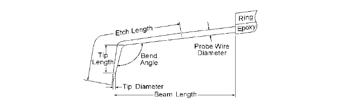
Many parameters are used to define probe geometry. Some of these parameters define the raw, straight wire, while others apply only to the finished probe. Some are determined by the application's environment, while others are best left to the discretion of the probe card designer. In general, the more parameters that are left unspecified, the greater the designer's flexibility to optimize the design for the manufacturing process without affecting performance requirements. The following discussion addresses some of the individual probe geometry parameters (Figure 17). Probe diameter, probe material, and etch rate influence the probe's spring characteristics and the resulting contact force.
Probe Wire Diameter
Wire diameter has the most significant effect on contact force and pad pitch. It's usually expressed in mils. Depending on the material used, available wire diameters range from six to 15 mils; however, small (<7 mil) and large (<12 mil) wire diameters are difficult to process and are generally avoided. The smaller wire diameters are required in cases where probe density and the number of probes are very high. The probe card designer determines the wire diameter to be used.
Etch Length
Etch length is a unit-less number used at the discretion of the probe card designer to vary the contact force. It's defined as the distance from the point where the wire diameter begins to decrease (usually in a linear fashion) to the tip of the probe. Refer to the probe geometry diagram in Figure 17 for details.
Bend Angle
The bend angle, which is expressed in degrees, is the inside angle of the probe after bending. The probe card designer chooses this value. The size of the angle used will determine the quality of the scrub mark the probe tip produces on the bond pad. Too wide an angle will cause the probe tip to skid off the bond pad without plowing through the oxide and making a good contact; too small an angle can cause the probe tip to punch a hole through the bond pad.
Tip Length
Probe tip length is measured from the tip of the probe to the bend in the probe and is expressed in mils (e.g., 7 mil tip length). The range of tip lengths on any given card is a function of the number of probe layers. The probe card designer determines tip length.
Tip Diameter
Probe tip diameter affects the contact resistance of the tip and damage to the bond pad. Larger tip diameters have lower resistance; however, for applications with aluminum pads, the larger tips require greater probe force to break through the pad oxide layer. Tip diameter selection is based on the size and material of the bond pad and is expressed in mils (e.g., 1.0 mil tip). This is the finished tip diameter after sanding, but when applicable, before radiusing (i.e., rounding of the tip). Tip diameters >4 mils require more production time and increase the cost because of the amount of sanding required, and are avoided when possible. As a guideline, when probing solder bumps, use a probe tip diameter that's at least as large as the diameter of the bump, because a tip diameter that's too small can dislodge or damage the bump.
Beam Length
On standard probe card designs, the beam length is dictated by the die size. On custom designs, the probe card designer chooses the beam length to meet contact force requirements. Beam length is expressed in mils (e.g., 200 mil beam length) and is measured horizontally from the center of the probe tip to the point at which the probe enters the epoxy (or for ceramic blades, the point the probe contacts the ceramic).
Probe Tip Shape
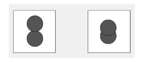
The shape of the probe tip influences both its contact resistance and the amount of bond pad marking or damage. Two shapes are available (Figure 18): flat or semi-radius (for some probe materials). Semi-radius tips require additional processing after sanding, so they're more time-consuming to produce.
Evidence suggests that reshaping all of a probe card's probe tips into smooth semiradiuses decreases scrub mark size, increases probe longevity, and produces cleaner wafer probing. Flat tip probes have a tendency to flake and disperse aluminum and oxide crystals across the bond pad. A smooth semi-radius probe tip provides a narrow scrub mark and breaks through the surface oxide with minimal flaking. Semi-radius probes also generally don't require abrasive cleaning, which increases probe life. However, when used over an extended period, semi-radius probes have a tendency to flatten out and take on the same characteristics as flat tip probes. My personal opinion is that the added cost and processing time aren't worth the short-term benefits and using tungsten-rhenium probes will produce very similar results.
Tip Etch
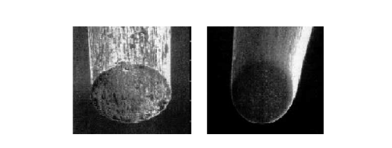
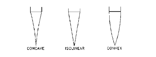
Ideally, an isolinear etch is preferable, but variations in the probe card manufacturing process can create a concave or convex etch (Figure 19). Over time, wear and abrasive cleaning can shorten the tip, increasing its diameter. A convex etch will accelerate this effect and reduce the useful life of the probe. On the other hand, a concave tip etch reduces the structural integrity of the probe tip and has a tendency to curl the tip unexpectedly.
Probe Tip Depth
Tip depth is a critical parameter for prober setup. It's the distance from the probe card's reference plane to the plane formed by the probe tips, generally measured from the bottom of the PCB to the probe tip. Tip depth is a function of the number of probe layers, ring thickness, probe angle, tip length, and beam length.
For a standard probe card design with a single layer of probes, 80+10 –5 mils is the accepted default. A greater tip depth is required for probing at temperatures ≥100°C. The default standard is 120+10 –5 mils. Designing a probe card with a tip depth that varies from the standards can require custom tooling and increased manufacturing time. High density designs generally require two or more layers to fit in the required number of probes and maintain acceptable clearances between them for manufacturing and application feasibility. Probe layer count can affect the achievable tip depth; however, in most parametric applications, a single probe layer is sufficient.
Maximum Probe Current
Many applications raise concerns about how much current a probe tip can handle. Pushing a probe beyond its limits can significantly reduce its life by scorching and burning the tip. It can even destroy an expensive probe card. The maximum allowable probe current is a function of probe material, probe wire diameter, probe tip diameter, and probe current duty cycle.
It's also important to take into account whether the probe currents used are continuous (steady state) or pulsed. Table 6 lists the maximum allowed steady state currents for the most common probe materials and tip diameters.
| Tip Diameter(mils) | Tungsten & Tungsten-Rhenium | BeCu | Paliney®7 |
| 1.0 | 120mA | 126mA | 134mA |
| 1.5 | 163mA | 172mA | 182mA |
| 2.0 | 202mA | 213mA | 226mA |
| 2.5 | 239mA | 252mA | 267mA |
| 3.0 | 270mA | 290mA | 310mA |
| 3.5 | 307mA | 324mA | 343mA |
| 4.0 | 340mA | 360mA | 380mA |
| 5.0 | 401mA | 423mA | 448mA |
Table 6. Maximum steady state current.
Some pulsed DC applications, such as HFE testing, may pass extremely high currents through the probes for short periods of time. When current is delivered in short bursts, probes can handle much more current than their steady state ratings would indicate. This assumes the probe tips are sanded flat for full surface contact and are clean and free of contamination. Improper contact or contamination on the probe tips can cause arcing and turn a probe tip into a mini arc welder.
Deriving the formulas for both steady state and pulsed current is somewhat complex and must take into account the electrical, dimensional, and thermal dynamics of the material in question. Refer to Table 7 for the final formulas. In the formula for ISS (steady state), "C" is a derived constant and is supplied for the three most common probe materials. The probe vendor should be able to supply this constant for any other type of material.Deriving the formulas for both steady state and pulsed current is somewhat complex and must take into account the electrical, dimensional, and thermal dynamics of the material in question. Refer to Table 7 for the final formulas. In the formula for ISS (steady state), "C" is a derived constant and is supplied for the three most common probe materials. The probe vendor should be able to supply this constant for any other type of material.
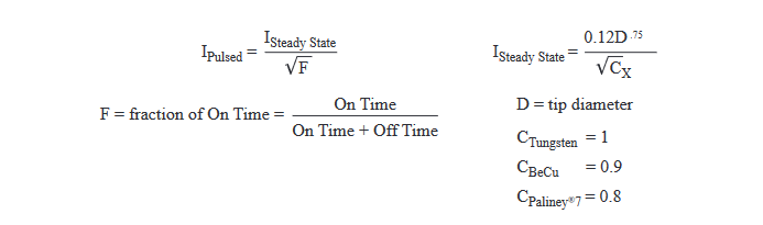
The maximum pulsed current formula is optimized for an ON time of £10msec. Where space allows, it's preferable to use multiple probes on one bond pad to pass high current. The additional surface area provided by multiple probes helps dissipate the heat generated from the transmission resistance of the probe and the current will be evenly distributed between the probes. Two 1.0 mil tips will provide more heat dissipation than a single 2.0 mil tip. In high current applications that employ epoxy ring cards, heat buildup in the probes can allow the epoxy to reach its thermal migration point, so it becomes soft and flexible, corrupting the positional accuracy of the probes.
Probe Card Parameters
Contact Resistance
Probe contact resistance (CRes) has become increasingly important as signal voltages drop, contact pressures decrease, and new devices based on technologies like gallium arsenide draw higher currents. Signal integrity has become even more dependent on probe contact quality. CRes is the interface resistance between the probe tip and the bond pad at overdrive. It's a function of the pad material, contact force, probe material, tip diameter, and tip shape.
CRes is generally not specified because actual CRes can't be measured easily. Instead, signal path resistance is often used because it's more relevant in most applications. Users will occasionally specify a nominal value for path resistance as a workmanship screen for cold solder joints or open circuits. Signal path resistance is the total resistance from the bond pad to the tester; i.e., the total of the contact, probe, solder connection, trace, and pogo/pin interconnect resistances.
The CRes of a probe in actual use depends heavily on pad material, the amount of scrub, and the condition of the probe, and can vary greatly from the nominal values. See Table 8 for nominal values of CRes on different bond pads. Only beryllium-copper, tungsten, and Paliney®7 are listed. Tungsten-rhenium is only slightly higher than tungsten.
| Beryllium-Copper | Tungsten 99.99% pure | Paliney®7 | |
| Contact Resistance | 100µΩ/gold 200µΩ/aluminum Excellent CRes.Stable and repeatable due to self-cleaning action. | 250µΩ/gold 250µΩ/aluminum Fair CRes. Unstable and unrepeatable due to build up of contaminants. | 100µΩ/gold 200µΩ/aluminum Excellent CRes.Unstable due to lack of planarity over use. |
| Fatigue resistance | Good | Excellent | Very poor |
Table 8. Nominal contact resistance values.
As mentioned previously, tungsten has a very loose crystal lattice structure. The fibrous nature of the tip is like a magnet for contamination, which leads to the unstable nature of the CRes value. Tungsten-rhenium has a tighter lattice structure and a smoother tip surface, which means the tip attracts less contamination and is easier to clean. Even though the CRes is slightly higher, tungsten-rhenium tips are a better choice than tungsten because the CRes is much more stable over time and use.
Contact Force
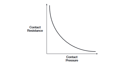
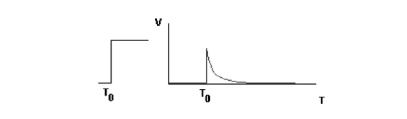
Probe contact force is defined as the force (measured in grams) exerted by the probe tip (measured in mils or microns) on the contact area. Tip force is primarily controlled by prober overdrive, increasing linearly with additional Z motion. Needle material, needle diameter, beam length, and taper length also play major roles in determining tip force. Figure 20 illustrates the relationship of contact force to contact resistance. Essentially, as the probe makes initial contact and begins to penetrate the surface layers of bond pad contamination and oxide, current flow begins quickly and increases as the probe tip contacts more subsurface bond pad metal. The contact resistance will continue to decrease as pressure increases, then level off to the nominal contact resistance of the two metals.
Contact force isn't normally specified or measured. However, if the user wishes to specify a contact force, it must be in the form of a balanced contact force specification. The actual contact force will be 1.0 to 2.5 grams/mil of overdrive floating average for tungsten or tungsten-rhenium probes with default characteristics and 0.5 to 1.6 grams/mil of overdrive floating average for beryllium-copper or Paliney®7 probes with default characteristics. Average contact force is the mean of all the probe forces, measured individually, for the entire probe card assembly, and is regarded as the nominal contact force of the probe card. Average contact force should be specified as a floating average or a range of acceptable values for the measured average. By letting the average contact force float within an acceptable range of values, the probe card design can be optimized with minimum variation in contact force. A contact force that is too high can damage the bond pads. A contact force that is too low may not be able to break through the oxide layer, producing unreliable test results.
Probe needle material contributes to contact force because the modulus of elasticity (stiffness) differs among materials. The probes bend and flex differently given equal overdrive and exert different amounts of force on the test pad. As probes are exercised over time, fatigue affects stiffness and results in changes in planarization. Tungsten is most resistant to fatigue and beryllium-copper (BeCu) is good, but Paliney® has poor fatigue resistance, so it's difficult to keep planarized.
Balanced Contact Force
Balanced Contact Force (BCF), measured as a "±%," is the allowable deviation from the floating average contact force. For example:
- ±50% of floating average with 10% sampled for measurement
- ±20% of floating average with 100% sampled for measurement
BCF is provided by ring design and careful selection of probe material and geometry parameters: wire diameter, tip diameter and shape, tip length, etch length, and beam length. If the user requests the BCF option (i.e., asks that the card manufacturer guarantee that all the probe needles fall within the specified contact force range), probes wear more evenly, and contact resistance and test results are more consistent. However, in most cases, the variation in contact force isn't measured. It should be noted that with proper selection of probe parameters, variation in contact force among the probes of the standard designs would generally be within ±20% of the average contact force.
By specifying a custom BCF <±20% or a non-standard floating average contact force, the user introduces requirements for custom tooling, tighter manufacturing tolerances, or a potentially un-manufacturable product and longer manufacturing times.
Overdrive
Overdrive is the amount of travel (vertical movement) after initial touchdown of the probes. The standard is one to three mils (25 to 76 microns). Proper overdrive of the probes ensures all probes are in contact with the wafer. Overdrive also provides the scrubbing action required to penetrate the oxide layer on the pad. The proper amount of overdrive for the application will depend on the tip shape, probe force, tip diameter, and planarity of the probes, as well as the type of bonding pad material used. Too little overdrive will result in high contact resistance and poor connections. Contact force increases as a function of overdrive, so excessive overdrive can not only produce device damage caused by microcracks under the test pad, but increases the wear on probe tips and reduce probe card life. The objective is to minimize overdrive to the extent that a reliable contact occurs between the test probe and the test pad.
Planarity
Probe test yield is the net increased result of fine-tuning all the various aspects of the probe test function. Probe to probe planarization is one of the most important aspects of probe card assembly, inspection and maintenance.
Planarity is the vertical distance between the highest and lowest probe tip on a probe card. This isn't a plus/minus measurement, but is specified as a total indicator reading (TIR). It defines the amount of vertical travel from the point where the first probe tip makes electrical contact to the point where the last probe tip makes electrical contact. For most standard bond pad configurations, maximum planarity won't exceed 1.0 mil (25mm) TIR. Tighter requirements are possible; however, increased maintenance and additional manufacturing time are required.
It's not uncommon for users of fixed pattern or low probe count probe cards to give little or no consideration to probe planarization. While everyone recognizes the importance of probe alignment and hitting the target, relatively little attention is given to probe-to-probe planarization. Planarization directly or indirectly affects a number of other contact test variables, such as contact pressure, contact resistance, and scrub length and depth. Device size and probe count are irrelevant to determining the necessity of planarization accuracy. Poor planarization will result in uneven contact pressure and accelerated probe tip wear on the lower probes. Although larger pad geometries provide plenty of room for scrub, poor planarization results in excessive overdrive, which leads to longer scrub marks, premature probe wear, overstressed and damaged probe needles, and probes that scrub off the pad.
Probe Alignment Accuracy
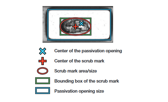
There are two definitions for probe tip alignment, which vary depending on the user's needs. Using a glass mask coordinate or bond pads on a wafer, alignment accuracy is the accuracy of the probe tip placement at overdrive with respect to the targets on the mask or wafer. When using a probe card analyzer, alignment accuracy is the position of the center of the scrub mark with respect to the center of the bond pad. Refer to Figure 21.
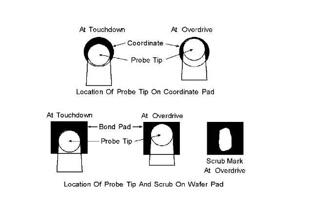
In either case, the entire scrub mark must be within the passivation opening and, to avoid contamination, the probe must not touch down before it reaches the opening. Refer to Figure 22. For the standard probe card, the specification is ±0.5 mils at rated overdrive if built to a glass mask; if built to a wafer, the probe tip is in alignment if the entire scrub mark lies within the passivation opening.
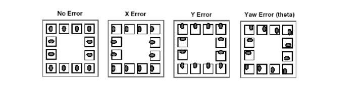
There are three common types of alignment errors: X error, Y error, and theta (rotational) error. Of the three error types, theta is the most likely to be caused by prober setup, rather than probe card assembly. XY alignment errors are the most common problem in probe card assembly. When examining a probed device, it's easy to spot probe misalignment because the scrub mark will be visibly off-center. See Figure 23.
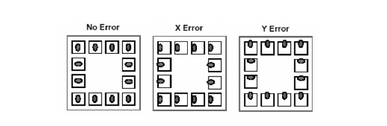
Alignment problems can indicate either a faulty prober setup or a probe card assembly problem. Referring once more to Figure 23, if all of the probes seem to be off in the same direction, then it's most likely a prober setup problem. When the probe marks on one side of the die are toward the outside edge of the pad and the other side of the die has the probe marks toward the inside of the die, then it's a theta error and the most likely problem is again the prober setup. Extra care taken to align the probes properly will help reduce setup costs, extend probe life, and increase device yield through faster setup and improved contact.
Tight pitch bond pads have increased the importance of accurate die pad coordinate information. Three different methods are available to convey coordinate information to the probe card vendor
- Sample wafer. The probe card designer measures the coordinates directly from the wafer using a digitizing station while viewing the bond pads with a video microscope.
- Hard copy. The coordinate values are manually entered into the computer system.
- Electronic. Die coordinates are delivered by floppy or email in an ASCII file in tabular format.
The accuracy of the probe tip position information used to manufacture a probe card is based on the cumulative accuracy of a number of factors: input data, template quality, operator skill, etc. All of these factors must be optimized in order to produce a card that requires a minimum of tweaking at final alignment and, therefore, reduced probe card manufacturing time. The best method of ensuring accurate data is conveyed is to provide the die pad coordinates in electronic format. There are a number of advantages to this approach:
- Allows the use of a probe card analyzer for verification.
- Reduces rework due to digitization or data reentry error.
- Improves quality due to less tip tweaking.
- Reduces data entry and design time.
Scrub Mark
Probe scrub refers to the sliding of the probe tip across the bond pad from the point where it first touches down to the point where it comes to rest at maximum overdrive.
Definitions vary from one device manufacturer to another. Some operations measure the length of the scrub mark from the center of the probe tip at touchdown to the center of the probe tip at maximum overdrive (scrub). See Figure 24. Others measure scrub length as the total length of the scrub mark (total scrub). Generally, the only requirement is that the scrub mark be within the passivation opening at full overdrive. Scrub length isn't specified.
Shrinking pad sizes make it difficult to keep the entire scrub mark on the bond pad. This is particularly true when the user requires that the probe tip must be centered on the target at maximum overdrive.
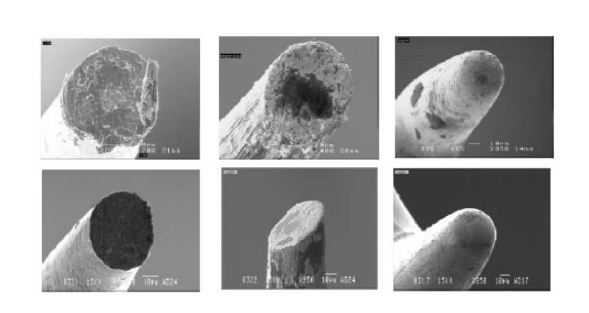
Scrub marks are the footprints left behind by the probe tips after contact with the test pad. While there are five visual characteristics associated with a scrub mark (Figure 25), there are more than forty different parameters that can be analyzed from these characteristics.
Scrub marks can provide valuable clues to a wide variety of probing difficulties. Careful visual analysis of the marks can assure quality control or point to potential trouble in need of corrective action. However, there are a variety of potential interpretations of the clues left by a scrub mark.
While probe planarization can be detected with a microscope that provides for depth perception, it's very difficult to view. Low probes, which contact the device first, will exert more contact pressure, will penetrate the pad surface deeper, and will produce a longer scrub length than higher probes. The longer scrub length means a lower probe tip will also tend to wear faster and may leave a snowplow type scrub mark.

This snowplow scrub (Figure 26) is the result of the probe tip penetrating the pad material. As the tip penetrates further, it pushes pad material forward, leaving a mound of pad material at the forward end of the scrub mark. In contrast, a high probe will have a shorter, shallower scrub mark due to the lighter contact pressure. The random combination of deep, wide, long marks with shallow, thin, short marks clearly indicates a planarization problem.
A worn probe will show up as a wider scrub mark and will also produce this snowplow pattern. In this case, the snowplow effect is due to the tip shape being worn flat over time. The flat tip shape tends to act like a chisel, digging under the pad material, lifting it up, and pushing it forward. Uneven wear on probe tips indicates planarization problems. Uniform excessive wear on the probe tips indicates that the probe card assembly has reached the end of its useful life.
Probe tip shape influences the quality of the contact and the shape and size of the scrub mark. The placement and the general qualities of the scrub marks provide feedback that gives the observant test engineer the opportunity to identify and correct many problems. Careful analysis of probe scrub marks allows the test engineer to monitor and improve the test performance greatly.
Probe Cards and High Temperature Testing
High temperature probing is defined as anything ≥100°C. It requires the use of special materials and special hot chuck alignment procedures. A high temperature probe card generally can't be used for ambient testing because of its special alignment characteristics. Even with the extra manufacturing steps involved in creating a high temperature probe card, the card's alignment at elevated temperatures tends to be unstable. In general, high temperature probing should be avoided; however, when it's required, keep the following considerations in mind.
First, let's consider the mechanisms of heat transfer. There are three types of heat transfer: radiation (red hot), conduction (touch), and convection (hot air rises). There is very little radiation at temperatures less than 300°C, so we ignore it. There is also very little conduction. Conduction requires a large area of contact. Contact area per needle is generally <1 mil2; therefore, a large number of needles would be required for significant contact area. The silicon wafer itself is the exception; the primary transfer of heat to the wafer is through conduction. This leaves convection, which indeed causes most of the heating.
Second, what parts of the system are exposed to this convection heating? Silicon wafer, probe needles, PCB, solder joints, probe card interface, pogo pins, probe card alignment pins in other words, all parts of the probe system are affected by convection heating. All of these systems use different types of materials and all of these materials have differing TCEs (Temperature Coefficients of Expansion). See Table 9.
| Material | Temperature Coefficient of Expansion |
| Silicon Wafer | 2.50 × 10⁻⁶/°C |
| Beryllium Copper | 7.78 × 10⁻⁶/°C |
| Tungsten Rhenium | 4.92 × 10⁻⁶/°C |
| Tungsten | 4.43 × 10⁻⁶/°C |
| Aluminum | 24.00 × 10⁻⁶/°C |
| Ceramic | 9.30 × 10⁻⁶/°C |
| PCB (FR4) | 13-18 × 10-6/°C |
| PCB (polyimide) | 12-16 × 10-6/°C |
| Epoxy (typical -25°C) | 65.00 × 10⁻⁶/°C |
| Epoxy (PTC125) | 25.00 × 10⁻⁶/°C |
Table 9. Probing material TCEs.
- All of the different parts of the probe system have different Temperature Coefficients of Expansion (TCEs), so as the ambient temperature rises and falls, nothing stays in one place for long.
- Material expansion plus mechanical constraints produce forces that cause twists, warps, and bends.
- The wafer expands, but not as much as the probe card
-Some critical materials (epoxy) develop undesirable characteristics; thy soften, affecting alignment stability, and become electrically conductive.
- Possible interference with alignment pins as card expands.
- The tester to probe card to prober interface for many systems is mechanically,thermally, and electrically complex.
- Interface stability is an important parameter when high accuracy probing is required. - Soak times
- Long soak time required for stabilization; top to bottom gradient will still exist.
- Uneven heating from moving chuck still causes probe card X-Y movement.
- Long soak times won't solve all the problems.
- There is some increase in the needle tip size due to conduction from the bond pad.This can affect long-term alignment stability.
These are just a few of the many issues involved with high temperature probing. It's a very complex issue and many problems remain unsolved. In the late ‘90s, SEMATECH formed a panel to address the issues of high temperature probing. Their primary focus was on functional die testing. Some of the progress made is transferable to parametric testing
Probe Needle Cleaning
Contact resistance is probably one of the biggest factors in probe yield loss. The increase in CRes is due to the buildup of contamination on the probe tips over time. Currently, the best way to enhance the long-term performance of the probe tips is to incorporate some type of periodic cleaning procedure. Scheduled cleaning procedures can help eliminate the yield loss due to the higher CRes. Probe cleaning is a hot topic within the industry and there is a large body of work being done in that area. The following paragraphs provide an overview of some of the issues associated with probe cleaning
Before deciding on a cleaning strategy, consider several points. Probe wear and cleaning frequency are the two major factors that determine useful card life. It's important to make decisions on the need for cleaning and the payoff based on the card's cost of ownership. Too much cleaning adversely affects throughput, reduces the life of the probe card, and increases production costs. Too little cleaning adversely affects test yields. See Figure 27.

The first and most obvious question is "How do I know if my probes are dirty?"
-
By visual inspection
- High contact resistance
- A re-probe failure rate that doesn't improve
- Yield fallout as a result of high contact resistance
The first clue that something is wrong is usually yield loss. Do a visual inspection under a microscope if dirty tips seem likely. Part of developing a cleaning strategy is understanding the testing process and the number of touchdowns that can be made before taking a yield hit. Figure 28 shows an example of dirty probe tips (top picture) and the same tips (bottom picture) that have been through a non-abrasive clean.
What are the sources of the contaminants?
- The primary culprits are aluminum and tungsten oxide
- Silicon nitride
- Electrically activated buildup of dielectrics
- Passivation
- Polymers and fluorocarbons
These contaminants accumulate on the probe tip and interfere with the surface contact and electrical contact of the probe. This causes the contact resistance to increase. Aluminum bond pads form an oxide coating instantaneously on exposure to air. High temperature probing dramatically increases the oxide build up on the pad. Gold bond pads can also develop a measurable contact resistance due to absorption of airborne contaminants on the surface, rather than chemical reactions with the gold.
Choose cleaning methods wisely. When deciding on a cleaning method, keep in mind the probe material and tip shape and consider how they will respond to the various cleaning methods. For instance, a flat tungsten tip is fibrous and contaminants can be impacted and embraced by these fibers. It probably wouldn't respond well to a dry brushing. Abrasive cleaning is rarely needed for BeCu, because it's a soft material and the tips wear down with use. BeCu would respond best to a non-abrasive technique. An abrasive cleaning technique would destroy a semi-radius tip.
Some of the methods used to clean the tips include:
- Scrub on a ceramic disk
- Scrub on tungsten carbide
- Scrub on 5m paper
- Touchdown on sticky paper
- Camel hair dry brushing
- IPA wet brushing
- Various solvents in high frequency acoustic tank
There are many different opinions about what works and what doesn't what should or shouldn't be done. Rather than advocating any particular method, this discussion was intended simply as an overview of the various cleaning methods, with the caveat that they all have their good and bad points. For example, abrasive cleaning works and doesn't require taking the card offline, but it reduces probe card life, causes deformation of the tips, and introduces the potential for additional contaminants. Wet and acoustic cleaning work as well as, or better than, abrasive sanding, but the probe card must be taken offline. Although chemicals and solvents can work, they are messy, destructive, must be done off-line, or their use is restricted in the test environment for safety or cost reasons. Sticky tape works well and can also be used online, but has some of the same restrictions as abrasive pads. After any major cleaning operation, the probe tips should be checked for alignment and planarization.
High Speed Digital and RF
High speed digital, RF, and microwave probing are complicated issues that are often best left to the experts in those areas. The purpose of this section isn't to make readers high speed experts, but to offer some idea of the issues involved, and enough information to know when to call in the experts. This topic will be discussed in two parts. The first part is a basic primer on high speed digital; the second part covers probing issues. Although I don't have any experience in RF and microwave design, I have done some high speed digital designs. Many of the basic concepts of high speed digital cross over into a basic understanding of RF and microwave.
There are six basic types of components in electronics, which can be divided into active components and passive components. Crystals, transistors, and diodes are active components; resistors, capacitors, and inductors are passive components. No matter how complex, every circuit or electrical device can be broken down into these basic components.
Probe cards are really nothing more than transmission lines. The three passive device types resistors, capacitors, and inductors make up the three major elements of an electrical transmission line.
High speed digital design studies how passive circuit elements affect signal propagation (in terms of ringing and reflections), interaction between signals (crosstalk), and interactions with the natural world (in the form of electromagnetic interference).
There are many ways to study passive components. Digital engineers use the step response, which illustrates what happens when a pulse hits a circuit element.
1. Resistor: A resistor is a device that opposes the flow of current in a circuit. It has two functions to limit current and divide voltages. Resistors display a flat response. At time zero, the output rises to a fixed value and holds steady.
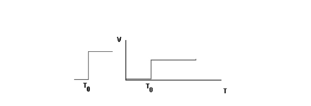
Resistor response to a step function.
2.Capacitor: Physically, a capacitor is any two conductive surfaces separated by an insulation-type material. It's capable of storing an electrical charge much like a battery. It takes time to charge and discharge. Capacitive reactance is the opposition to a change in voltage. Capacitors display a rising step response. At time zero, the output starts out at zero but then later rises to full valued output.
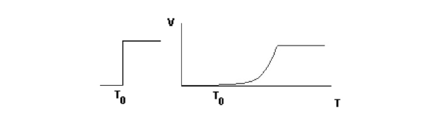
Capacitor response to a step function.
3. Inductor: Current flowing through a conductor creates a magnetic field. The initial energy of current goes into creating this field and takes time. When the current stops, the field collapses and induces the current to continue flowing. Inductive reactance is the opposition to any change in current. Inductors display a sinking step response. At time zero, the output rises instantly to full value and then later decays back toward zero.
Inductor response to a step function.
Clock speed doesn't equal bandwidth. There are many high frequency harmonics that add together to make up that clock pulse. Square waves, as illustrated in Figure 29a, can be thought of as a combination of a series of sinusoidal waveforms that are odd-numbered harmonics of the square wave fundamental.
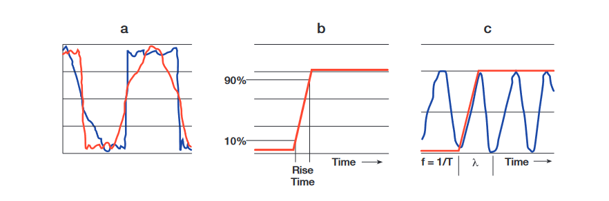
Figure 29b illustrates a common logic pulse transition from a low level to a high level, defined here as the time to transition from 10% to 90% of the total magnitude. As shown in Figure 29c, if a sinusoidal waveform is overlaid on the logic pulse, the rise time turns out to be almost 30% of the period of the sinusoidal waveform. Given that the frequency equals the reciprocal of the period, a one nanosecond rise time might generate a brief 400MHz transient of the same peak-to-peak amplitude. This logic pulse could be a 10MHz clock frequency, but the bandwidth would have to be much greater than 10MHz in order to pass the pulse without any distortion.
In the probe world, the most difficult frequencies to deal with are in the gigahertz range. So, how is it possible to gain a rough idea about the bandwidth involved from the rise times? The first step is to learn a little bit about spectral energy. The knee frequency is that point in the spectral energy where the spectrum attenuates much faster than the natural 20dB/decade roll-off. The knee frequency for any digital signal is related to the rise (and fall) time of its digital edges and not its clock rate. The clock rate is generally just inside the 3dB point. The behavior of a circuit at the knee frequency determines its processing of a step function. This information makes it possible to make a rough estimate for digital spectral energy. See Figure 30.

Fknee = the frequency below which most energy in digital pulses is concentrated Tr = the pulse rise time. Shorter rise times push Fknee higher. Longer rise times pull Fknee lower. The important time domain characteristics of any digital signal are determined primarily by the signal's spectrum below Fknee. From this principle, we may deduce two important qualitative properties of digital circuits:
- Any circuit that has a flat frequency response up to and including Fknee will pass a digital signal practically undistorted.
- The behavior above Fknee of a digital circuit will have little effect on how it processes digital signals.
When using this formula, keep in mind that it's an imprecise measure of spectral content. Used as a guidepost, Fknee can help classify frequency-sensitive effects as totally insignificant, merely worrisome, or completely devastating. For most digital problems, that's all that's required.
Fknee has its limitations. It's no substitute for full-blown Fourier analysis and can't make precise predictions about system behavior. However, for digital signals, Fknee quickly relates time to frequency in a practical and useful manner.
Energy Wave Characteristics
- Energy waves can be continuous like ocean waves or short bursts (pulses).
- Energy waves take time to travel from one point to another.
- Energy waves can be absorbed or reflected.
- Energy waves attenuate as they travel.
- Energy waves can be channeled to flow along a specific path.
- The velocity is dependent on the medium through which the energy wave travels.
Ringing is the term used when impedance mismatch between lines causes reflections.When a pulse reaches the end of a line at a load, connector, or where a line splits, reflection and scattering occur. Subsequently, a further reflection occurs when the pulse returns to the input. One can visualize the effect by recalling the high school physics lab wave tank, where a liquid is reflected back and forth through the tank. The resulting reflections are cumulative, with the reflecting signal reducing the signal integrity with each pass.
Crosstalk can occur when adjacent signal lines interact. When a voltage is present on a signal line, an electric field emanates from the line. This field can capacitively couple with adjacent lines, causing unwanted interaction. The amount of crosstalk between adjacent lines depends on the distance between the lines, the length of parallelism, and the level of energy in the transmitting line.
Probing Issues
Controlling the physical dynamics of probing high speed devices precisely demands special attention to detail. The degree to which these elements are controlled will directly affect the degree of success and the yield achieved. Probe card technology has struggled to keep pace with increasing frequencies and speeds. The card styles and connectors that are required are changing the character of the probe industry from off-the-shelf generic probe cards to application-specific custom probe card designs. The solution to successful probing ofhigh frequency, high speed devices will most likely come from a cooperative effort between the device designer, the production test engineer, and the probe card design specialist. Custom designed, application-specific probe cards offer the best opportunity for success.
Designing a high frequency probe card means bridging the traditional separation of conceptual design and physical implementation. In these applications, physical layout is intimately associated with circuit performance and the test results obtained. Designers of high frequency probe cards will have to take into consideration the geometric features of the physical layout. Etch length, width, thickness, spacing, and via placement all have a direct effect on performance.
By the very nature of its construction, a printed circuit board is a big collection of inductors and capacitors. Every conductor (trace, via, plane, etc.) has some inductance that opposes any change in current. Capacitors are also formed at every location where conductors are in close proximity to each other. This can be conductors located side-by-side or conductors on nearby layers. The wider a conductor is, the larger the capacitance will be. The closer the conductors are to each other, the more capacitance there will be. The capacitors and inductors that are formed as an integral part of the board structure are referred to as the distributed capacitance and inductance of the board.
Ground planes are used extensively, both as inner layers and on the external surface of the card. The external ground plane often serves as an EMI shield and provides a way to attach a coax shield for improved grounding. The inner ground plane also can serve as a common ground and reduce capacitive coupling between traces on either side of the board. More importantly, the inner ground plane provides more accurate control of characteristic impedance. The value of characteristic impedance depends mainly on the width of the trace conductor and its distance from the ground plane(s). The ability of multilayer probe cards to provide transmission line characteristics has made them increasingly valuable in high speed applications.
What can the device engineer do to improve probing and testability?
-
Must have DC ground return pad on each side of the chip to be probed: Prevents bias oscillations.
- Must have RF ground adjacent to RF signal pads: Good RF launch onto the chip
- Must tie all grounds together on chip to eliminate common lead inductance: Prevents common lead inductance-induced RF degradation.
- RF pad spaced logically around the chip perimeter: Allows signal isolation and mechanical spacing for relatively large probes.
- Must use standard RF signal footprint for pads (G-S-G or G-S): Allows common use of probes in all RF applications.
The preceding information gives a very clear picture of the complexity of assuring signal integrity through the probe card. The probe, however, represents the "business end" of the test fixture, so it's critical that it be able to transfer the signal without loss or degradation.
Summary of probe needle concerns and requirements:
- Tight control of alignment and planarity: Improves accuracy and repeatability, and reduces contact resistance through good contact.
- Proximity of ground pads on chip launch (directly from G-S or G-S-G layout): Needed to launch signal properly and maximize controlled impedance path.
- Controlled impedance of entire path, as well as probe-to-probe coupling and shielding: Reduces reflections and interfering signals.
- Low RF/microwave probe loss to source/receive for desired signals: Many devices require higher power, >0dB, at probe tip.
- Proximity of decoupling caps and low series inductance: RF and microwave have a tendency to easily oscillate.
Typically, smaller diameter needles and longer extensions are selected when probing high frequency devices in order to reduce tip force and resulting device damage. However, beam length also becomes a contributing electrical factor where the needle becomes an electrical performance component. Shorter beam length provides lower inductance and capacitance. The needle ultimately selected will usually represent a reasonable compromise between all these conflicting variables.
Several probe technologies in use today are, to a greater or lesser degree, suitable for probing high frequency devices. The key performance characteristics to consider are planarization accuracy and its effect on contact force, contact resistance, probe to probe capacitance for reduced crosstalk, and the ability to maintain signal integrity through the probe to the bond pads.
Successful probing of high frequency devices is a result of mastering both the mechanical as well as the electrical properties of the probes and the probe cards. It's extremely important that device design engineers, test engineers, and the probe card designers work cooperatively to bring about unique solutions for testing these devices.
Glossary
ATE - Automatic Test Equipment.
BALANCED CONTACT FORCE - Measured as a "± %," BCF is the allowable deviation from the floating average contact force
BEAM LENGTH - The distance, measured horizontally, from the center of the probe tip to the point the probe enters the epoxy.
BLADE CARD - A type of probe card that uses ceramic or metal blades to support individual probes.
BOND PAD - The metalized locations on an integrated circuit where the test probes will make contact.
BOND PAD PITCH - The distance between adjacent bond pad centers.
BOND PAD SIZE - The measurement of that portion of the bond pad metalization that's usable for probing. Also known as the passivation opening.
BURST CURRENT - A current pulse of less than 10ms duration.
CONTACT FORCE - The force presented by a probe at overdrive on a bond pad or bump,measured in grams/mil of overdrive (OD).
CONTACT RESISTANCE - The resistance that occurs at the junction between the probe tip and the device contact surface metalization.
DIELECTRIC CONSTANT - A measure of the ability of a material to resist the formation of an electric field within it.
DIELECTRIC LOSS - A measure of signal loss due to dielectric materials that is slightly conductive, even at DC, and due to the polarization process dissipating energy at higher frequencies.
DIE - A single square or rectangular piece of semi-conductor material onto which a specific electrical circuit has been fabricated. Plural is dice. Also called a chip.
EDGE SENSOR - An edge sensor (E/S) is a two-wire or three-wire probe configuration that forms a switch to detect contact with the wafer.
FLOATING AVERAGE - A range of acceptable average values. Applies specifically to contact force.
FR4 - A PCB material (glass epoxy) that is used for probe cards designed for probing temperatures less than 100°C.
GLASSIVATION - Passivation using silicon dioxide (glass) as the coating.
LEAKAGE CURRENT - Parasitic loss of current in an electrical circuit.
MASK - A patterned screen, usually of glass, used to allow exposure of selected areas of photoresist-coated wafer by a light source.
MICRON - A metric unit of linear measure that equals one-millionth of a meter. Same as micrometer (mm); equal to 0.0394 mils.
MIL - One thousandth of an inch. Equal to 25.4 microns.
OHM (Ω) - Unit of measurement used for resistance.
OVERDRIVE - Z-axis (vertical) distance measurement calculated from the first contact point of the probe to the device surface.
PALINEY®7 -A precious-metal alloy comprised of gold, palladium, platinum, silver, copper and zinc, which is used for making probes. Paliney®7 is a registered trademark of the J.M. Ney Company.
PASSIVATION - A protective coating placed on a wafer surface. Sometimes called glassivation.
PCB - Acronym for PRINTED CIRCUIT BOARD.
PCB APERTURE - A hole opened in the center of a PCB to support attachment of the ring.
PLANARIZATION - The ideal probing operation would result in simultaneous contact of all test pads on each and every device across the substrate. It would be a planarized system.
POLYIMIDE - A PCB material that is used for probe cards designed for probing temperatures greater than 100°C.
PROBE ANGLE - The angle of the probe shank where it passes through the epoxy relative to the horizontal plane of the PCB.
PROBE CARD ANALYZER - A piece of test equipment used to measure critical probe card parameters.
PROBE FANOUT ANGLE - The angle made by a probe with respect to the side of the die, measured from the perpendicular to the die side.
PROBE SHANK - The portion of the probe that isn't tapered.
PROBE SOLDER POINT - The location on the PCB where the probe tail is connected.
PROBE STABILITY - The ability of a probe to retain its performance characteristics over time.
PROBE TAIL - The portion of a probe outside the ring.
PROBE TIP ALIGNMENT - Probe tip placement at overdrive with respect to the targets on a coordinate glass mask or bond pads on a wafer.
PROBE TIP DEPTH - The distance from the reference plane of a probe card to the plane formed by the probe tips. This is typically measured from the bottom of the PCB to the probe tips.
PROBE TIP LENGTH - The vertical distance from the tip of the probe to the bend in the probe.
PROBE TIP SHAPE - The contour of the probe tip; typically flat or radiused.
PROBE WIRE DIAMETER - The diameter of the wire material from which the finished probe is made.
PROBING - A term used to describe the electrical testing that employs very finely tipped probes applied sequentially to a wafer.
RING - A ceramic or aluminum piece machined to proper dimensions to support probes on a PCB.
RING APERTURE - The opening (hole) in the center of the ring.
SCRUB MARK - Mark on the contact surface created by scrubbing action as the probe tip moves across the device metalization when over drive is applied.
SIGNAL PATH RESISTANCE - The total resistance from the bond pad to the tester; i.e., the total of the contact, probe, solder connection, trace, and pogo/pin interconnect resistances.
TARGET - A shape on a glass mask that represents the final position of the probe tip.
TIP LENGTH - Probe tip length is measured from the tip of the probe to the bend in the probe.
TIR - Acronym for Total Indicator Reading, expressed as an absolute value rather than a "±" value.
TOUCHDOWN - (1) The point of initial contact between probe and bond pad. (2) The number of times (touchdowns) the probe card is overdriven onto a wafer during the lifetime of the probe card.
WAFER - A thin disk of semiconducting material (usually silicon) on which many separate circuits can be fabricated and then cut into individual ICs.
YIELD - The number of acceptable units produced compared to the maximum number possible.