Introduction to High Voltage Capacitance-Voltage (C-V) Testing
Due to the complexities typically associated with high voltage (1 kV) capacitance wafer-level testing, such as instrumentation setup, cabling, probing, automation, and safety, on-wafer, 1 kV C-V testing is usually limited to characterization labs or manual benchtop setups that are separate from a fab’s standard production workflow. This application note contains implementation details on the integration of 1 kV C-V testing into a production environment using Keithley’s S530-HV Parametric Test System.
Keithley’s S530 is a production and lab system used for DC and C-V parametric testing of semiconductor devices. There are several versions of the system including low voltage (< 200 V) and high voltage (HV) systems. The HV system is widely used for power device characterization in the production environment.
This new HV C-V capability is released in the Fall of 2021. It requires KTE 7.1 and new bias tees.
Power device characterization (Cout, Cin, Cgs, Cds, Cgd)
C-V characterization is a critical measurement for semiconductor devices, much like gate oxide capacitance (COX) measurements—one of the few measurements that allows direct characterization of gate oxide thickness (TOX). These measurements do not require high voltage bias.
With the development of power electronics, high voltage capacitance measurements became a requirement for power device characterization and specification control. For instance, measuring Cin and Cout of power transistors allows engineers to characterize switching speed and power dissipation of high voltage power transistors.
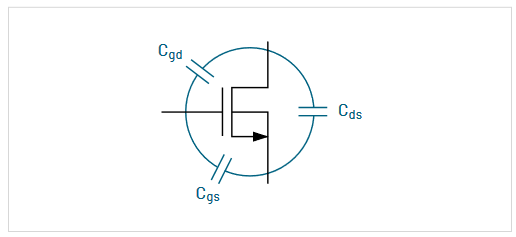
The switching speed of the power devices is controlled by the device’s capacitances. Figure 1 illustrates the capacitances between gate and drain (Cgd), gate and source (Cgs), and drain and source (Cds). Figure 2 shows the combination of these capacitances (Ciss, Coss, Crss) that characterizes the input and output transient performance. Ciss (Cin) is equal to Cgs plus Cgd. The Cin capacitance must be charged for the transistor to be switched on and it controls the speed of the turn-on switching. Coss (Cout) = Cds + Cdg is an output capacitance. It affects circuit resonance and dynamic behavior. Crss (Cgd) is the reverse transfer capacitance, sometimes called Miller capacitance. This capacitance controls turn-off timing.
The switching speed of the power devices is controlled by the device’s capacitances. This includes capacitances between gate and drain (Cgd), gate and source (Cgs), and drain and source (Cds). The combination of these capacitances (Ciss, Coss, Crss) characterizes input and output transient performance. Ciss (Cin) is equal to Cgs plus Cgd. The Cin capacitance must be charged for the transistor to be switched on and it controls the speed of the turn-on switching. Coss (Cout) = Cds + Cdg is an output capacitance. It affects circuit resonance and dynamic behavior. Crss (Cgd) is the reverse transfer capacitance, sometimes called Miller capacitance. This capacitance controls turn-off timing.
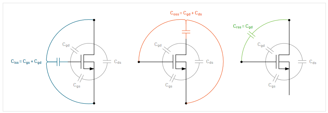
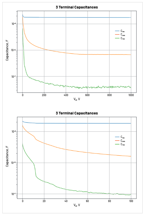
Figure 3 shows two graphs of Ciss, Coss, and Crss as a function of Vds, as measured by the S530-HV system. Ciss, Coss, and Crss are measured in the off state, when Vgs = 0, for different drain (Vds) biases.
Basics of C-V Measurements
Outline of measurement technology
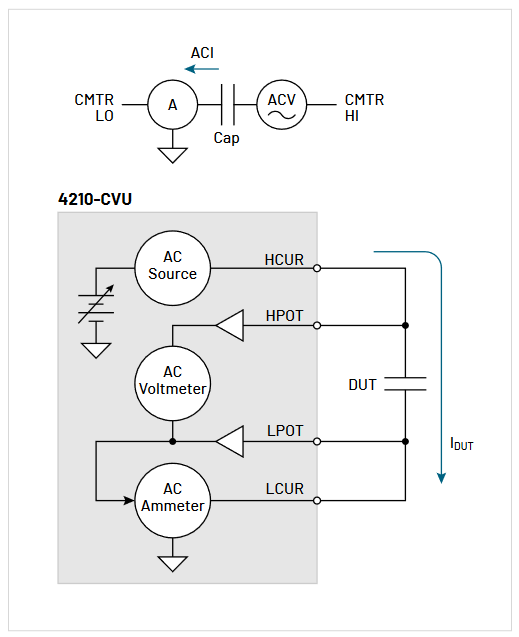
Figure 4 illustrates how AC impedance meters characterize capacitance. AC impedance meters are usually called C-meters (CMTR). These meters consist of two parts, the high side, CMTRH, and the low side, CMTRL. The high side is connected to one side of the device, and it forces AC voltage (ACV) of known amplitude and defined frequency. Common frequency values in a production environment are 100 kHz and 1 MHz. The low side tries to enforce 0 AC voltage by supplying the required AC current to balance the bridge.
By measuring the ratio and phase difference between forced ACV on the high side of the device to the induced AC current (ACI) measured on the low side of the device, the instrument calculates the complex impedance of the device.
Current Measurement
As previously mentioned, C-meters do not directly measure capacitance. Instead, they measure current, and by comparing the current to the voltage, they can characterize AC impedance. This impedance can be easily converted to the desired impedance vector pair. For example, it can be expressed as Cp and Gp, or Cs and D, or R and X.
The CVU can measure and display the following parameters:
- Impedance and phase angle (Z, Theta)
- Resistance and reactance (R + j X)
- Parallel capacitance and conductance (Cp–Gp)
- Series capacitance and resistance (Cs–Rs)
- Parallel capacitance and dissipation factor (Cp–D)
- Series capacitance and dissipation factor (Cs–D)
Cp (parallel model capacitance) is usually used to extract gate oxide thickness. For power devices, more complicated setup and models are used to extract Cgs, Cds, and Cgd.
S530 systems use a Keithley C-meter integrated within the 4200A-SCS Parametric Analyzer. Since 2021, all systems were integrated with the 4215-CVU Capacitance Voltage Unit. Previous models used the 4210-CVU.. The 4215-CVU supports a larger set of frequencies with a 1 kHz frequency step and can generate ACV up to 1 V. The 4210-CVU card is limited to 100 mV.
Both cards have the same three current measurement ranges, 1 µA, 30 µA, and 1 mA. The lower the range, the lower current it can measure. Meanwhile, the high current ranges are faster. The noise floor of each current range is five to six digits, depending on the PLC and filter settings.
Signal to Noise considerations
Impedance measurements have multiple controls that impact speed and accuracy. The most important parameter is the current range. Speed and accuracy are impacted by the frequency, ACV amplitude, integration time (power line cycles, PLC), and filter parameters. ‘Figure-of-merit’, or intrinsic performance, is controlled mostly by the current range, frequency, and ACV amplitude.
It is easy to estimate the accuracy of the C-V measurements for given conditions. For example, if the capacitance under test is C, then ACI will be equal to:
ACI = C * 2 * π * Frequency * ACV
or if C = 10 pF, Frequency = 1e5 kHz and ACV = 30 mV, then ACI ~1.9e-7 A
If the current range is 1e-3, and a low PLC is used, then the accuracy will be in the range of five significant digits, or about 1e-8 A, and the ratio of the noise current to the device current will be about 1e-8/1.9e-7 ~ 5%. That means that at these conditions, it is difficult to expect better accuracy than 5%. This accuracy can be improved by increasing the test frequency and ACV as well as by decreasing the current range.
PLC and filter settings can make measurements more accurate at the expense of the test time. This improvement has statistical origin, and the improvement of the signal-tonoise ratio is inversely proportional to the square root of the test time, and therefore is not very effective:
Signal/Noise = ~ 1/sqrt (test_time)
Square root dependency means that if you want to decrease noise by 10× by changing PLC or filtering—with no change to frequency, current range, or ACV amplitude—the test time has to be 100× longer, which is not practical. Other parameters like frequency, current range, or ACV amplitude should be used to improve signal-to-noise ratio.
With standard MOS silicon devices, you shouldn’t use Ac voltages higher than 30 mV. High ACV values change the shape of the C-V curve. For power devices, the capacitance is not highly dependent on the voltage, so higher ACV values improve the signal-to-noise ratio.
Bias tees
C-V characterization of a single MOS capacitor or characterization of a transistor requires the application of DC bias conditions across the device. This functionality is included in the CMTR circuitry. The impedance meter mixes AC and DC signals before applying a combined signal to the DUT. It is accomplished through the use of internal bias tees (Figure 5) integrated into the instrument.
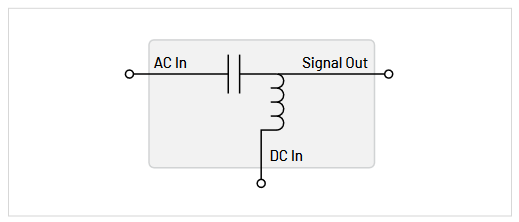
Keithley CVU cards integrated within the 4200A-SCS can supply up to ±30 V. This bias voltage can be applied to each of the C-V ports (both CMTR low and CMTR high). As a result, it is possible to have 60V across the capacitance in a differential setup. For power devices, this bias is not sufficient and external bias tees and power supply are needed.
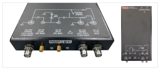
Keithley has developed a model of bias tee (S530-RBT-1KV), pictured in Figure 6, that can sustain bias voltage up to 1.1 kV. In the S530HV system, the bias voltage is provided by a Keithley 2470 Source Measure Unit (SMU) that has a maximum voltage of 1100 V. This bias tee also has two AC connections for “AC IN (CUR)” and for ‘AC IN (POT).” The bias tee also has two Kelvin connections to the DUT to maintain a four-wire connection up to a probe card. A diagram of a bias tee with Kelvin connections is shown in Figure 7.
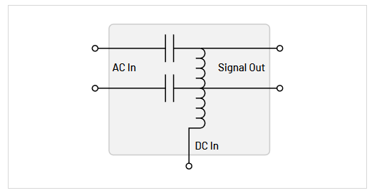
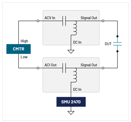
Figure 8 shows a diagram of testing a two-terminal capacitance with the use of two bias tees. The top bias tee take input from the high side of CMTR (ACV drive) and DC ground and delivers this mixed signal to the high side of the capacitor. The low bias tee provides HV DC bias to the DUT and provides a low AC impedance path to the low side of the CMTR, which is usually the sense-side of the CMTR, and measures ACI.
Connection setups for threeterminal measurements
C-V measurements on power devices are more complicated because you need to individually measure Cgs, Cds, and Cgd(Figure 1). These three measurements impact each other, make measurement difficult and decrease accuracy
Let’s consider the diagram in Figure 9 as a possible connection scheme to measure Cgs. Note that there is a parasitic path for AC from the source to the drain and then to the gate. This current can potentially be suppressed by providing a low AC impedance path of drain connection to the ground. However, in this case, the 2470 SMU is connected to the drain to provide drain voltage and does not represent a low AC impedance path to the ground. The drain in this case is not properly AC guarded. Therefore, we do not recommend similar connection setups to measure individually Cgs, Cds, and Cds. Instead, we suggest measuring Cin/Ciss, Cout/Coss, and Cgd/Crss (Figure 2).
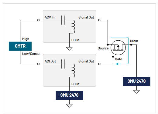
Measuring Cin
The diagram in Figure 10 shows the connection setup for the Cin (input capacitance) measurement. The setup allows independent control of Vgs and Vds (DC biases). ACV is applied to the drain and source and ACI is the measurement from the gate. This setup does not require AC guarding, but the measured value Ciss is equal to Cgd + Cgs. This measurement alone will not return all capacitance values (Cgs, Cgd, and Cds). Independent measurement of Cgd (described in the next section) will be needed to extract the capacitance between the gate and source (Cgs = Cin – Cgd).
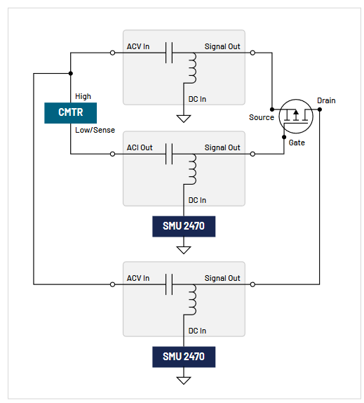
Measuring Cout
The diagram shown in Figure 11 is the recommended connection setup for Cout (output capacitance) measurement. It is very similar to the Cin setup, but the gate and drain’s connections are swapped. The setup allows independent control of Vgs and Vds (DC biases). ACV is applied to the gate and source and ACI is measured at the drain. The setup does not require AC guarding. The value Coss is equal to Cgd + Cds. This measurement alone will not return all capacitance values (Cgs, Cgd, and Cds). Independent measurement of Cgd (next section) has to be done to extract Cds from Cout as Cds = Cout - Cgd.
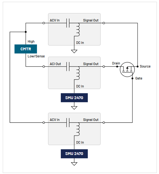
Measuring Cgd
Measurement of Cgd is the last measurement according to the suggested technique. This measurement allows calculation of Cgs and Cds from Cin and Cout. The same configuration of bias tees is used as shown in Figure 12. There is one important difference between the Cgd configuration and the Cin and Cout configuration: the source has to be AC guarded. AC guarding means the impedance between the device terminal connection (source) and the ground is low. The quality of AC guarding is important to suppress parasitic conductive paths around the source. For Cgd, this can be achieved because the source terminal can be directly grounded. However, precautions must be taken to ensure low resistance between the source and ground. This means you need low resistance cable connections and matrix connections, and you must minimize contact resistance to < 0.1 Ohm.
Three bias tees, the CMTR, and two 1 kV SMUs can be connected in a fixed configuration, which allows engineers to measure Cgs, Cds and Cgd without a connection change between the device, SMUs, and CMTR. All configuration changes can be done by changing the connection of the three bias tee output terminals between the ground and the three pins: gate, source, and drain. This connection change can be done automatically using a 1 kV switch matrix.
S530-HV 1 kV Test System
Architecture, matrix connection
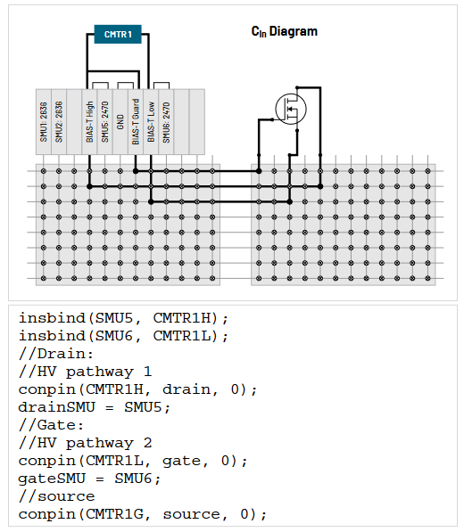
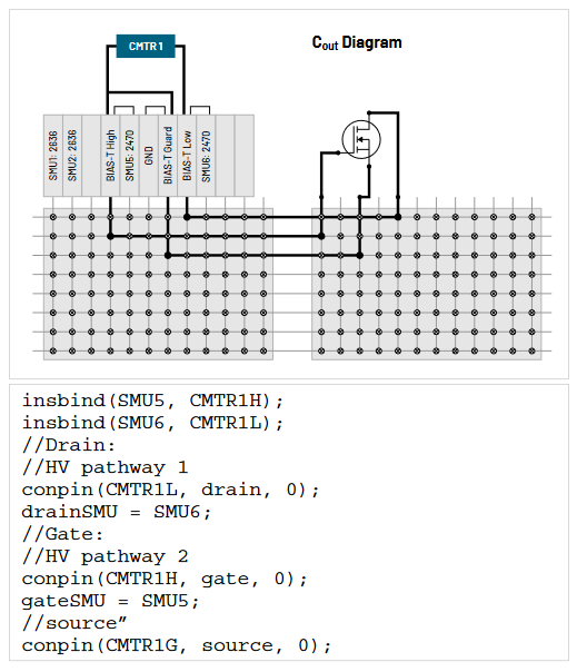
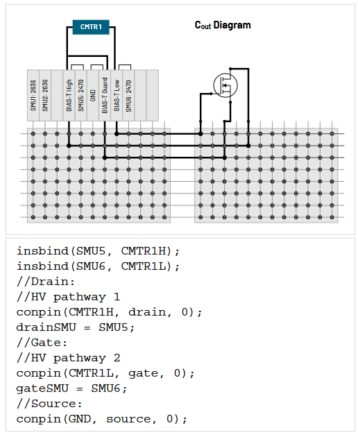
Figure 13: Matrix connections diagrams for Cin, Cout, and Crss.
In the above code standard LPT functions are used, including ‘insbind’. This ‘insbind’ function in the context of HV C-V performs the following actions:
- ‘binds’ CMTRL/CMTRH/CMTRG to the appropriate HV SMU, consistent with icconfig_QMO.ini definition. “bind” operation makes a single ‘instrument’ from appropriate SMU and CMTR.
- If different SMU is used, LPT generates an error
- Switches output of 2470 to the Front connection and allow DC signal to connect to bias-tees. Matrix connections of SMU are not used. Front connection changes automatically to Back connection after devint().
Here it is assumed that CMTR1 is High Voltage C-meter, and system also may have Low Voltage CMTR (CMTR2).
We have seen that switching from Cin to Cout and Cgd measurement setups only requires changing the connections of the three-terminal transistor to the output terminal of bias tees. Figure 13 shows how requirements of the connections described in Figures 10–12 are implemented by matrix connections and corresponding sample of code. Please note that the system configuration with the matrix includes the following aspects:
- Bias tee high, Bias tee low, and Bias tee guard are treated as separate instruments.
- CMTR is not connected to the matrix. Instead, it is connected directly to the AC inputs of the bias tee. The high side is connected to both bias tee high and bias tee guard. The low side of CMTR is connected to bias tee low.
- Bias tee high and bias tee low get DC voltage from a front connection of two 2470s, which are usually unused.
- The 2470 SMUs, by default, are connected to the matrix as regular system instruments using rear SMU outputs. Front outputs are used in HV C-V applications. The ‘insbind(SMU5, CMTR1H)’ command switches outputs to the front connections, which are hardwired to bias tee input DC terminals.
- Note that the bias tee high and bias tee low are using pathways 1 and 2 only. These top pathways are high voltage pathways. If these connections follow previous ‘conpin’ statement to other LV instruments, or gnd, high voltage pathways already will be used up, and software will generate an error. HV connection has to be done first.
- Here, bias tee guard gets its DC connection as a hard connection to the ground. As an alternative (it is not shown here), bias tee guard can be connected to one of the output pins of the matrix. Then, bias tee guard can be connected either to the system ground or to LV SMUs, such as the Keithley 2636B SMU. This configuration would provide more flexibility for DC biasing but will use one extra pin.
Architecture, alternative matrix connections (not recommended)
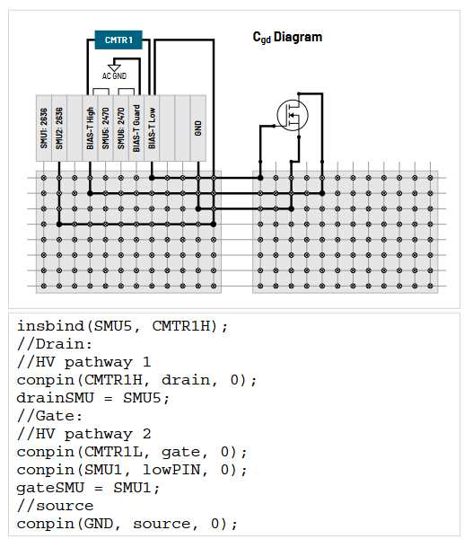
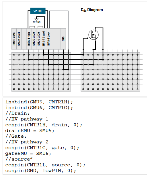
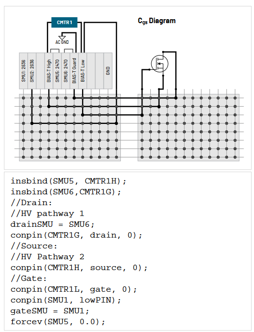
Figure 14: Matrix connections diagrams for Cgd, Cds, and Cgs.
This alternative system configuration is not recommended because it directly measures Cgs, Cds, and Cgd by AC guarding the third terminal. For example, to measure Cgs, the drain has to be connected to bias tee guard. And while this is an AC path to an AC ground, it is not a direct path to the ground.
Please note that in this configuration:
- Cgs, Cds, and Cgd are measured directly by AC guarding the third terminal.
- Bias tee high is connected to the 2470 SMU and CMTRH.
- Bias tee low is connected to CMTRL and one of the matrix pins, which supplies voltage below 200 V.
- Bias tee guard is connected to the 2470 and AC terminated to provide a low AC resistance path to the ground. AC resistance can be estimated approximately equal to a 160 nF capacitor.
- Bias tee high and bias tee guard use the first two HV pathways of the matrix.
Feasibility testing of three-terminal transistors, verifications
A three-terminal capacitance measurement is difficult to make, primarily because three capacitances are in one single circuit and it is impossible to break the circuit to characterize Cgs, Cds, Cgd individually. While it is possible to properly AC guard one of the terminals—such as the source terminal for Cgd measurements—it might not be very clear how effective the AC guarding is and how much AC current leaks through the parasitic path.
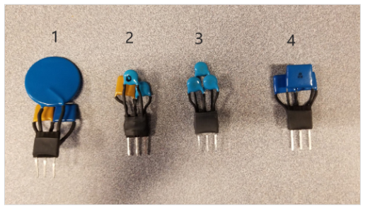
To address the problem, four sets of various capacitances were characterized before three-terminal C-V measurements were made with test parts (Figure 15) to determine the effectiveness of using three-terminal transistors. The experiment contained four different parts with values shown in Table 1.
| 100 kHz | Part #1 | Expected | Actual | Error | |
| Cgs | 9.730E-10 | Ciss | 9.838E-10 | 1.0218E-09 | 3.9% |
| Cds | 1.023E-10 | Coss | 1.132E-10 | 1.1811E-10 | 4.4% |
| Cgd | 1.081E-11 | Crss | 1.081E-11 | 1.1523E-11 | 6.6% |
| part #4 | |||||
| Cgs | 4.660E-09 | Ciss | 4.671E-09 | 4.8457E-09 | 3.7% |
| Cds | 1.086E-11 | Coss | 2.174E-11 | 2.3740E-11 | 9.2% |
| Cgd | 1.088E-11 | Crss | 1.088E-11 | 1.2298E-11 | 13.0% |
| part #3 | |||||
| Cgs | 9.316E-10 | Ciss | 1.863E-09 | 1.8790E-09 | 0.9% |
| Cds | 9.270E-10 | Coss | 1.858E-09 | 1.8885E-09 | 1.6% |
| Cgd | 9.310E-10 | Crss | 9.310E-10 | 9.3768E-10 | 0.7% |
| part #2 | |||||
| Cgs | 9.460E-10 | Ciss | 1.050E-09 | 1.0556E-09 | 0.6% |
| Cds | 9.390E-10 | Coss | 1.043E-09 | 1.0487E-09 | 0.6% |
| Cgd | 1.036E-10 | Crss | 1.036E-10 | 1.0694E-10 | 3.2% |
Table 1: Sample evaluation data for 100 kHz test frequency.
The second column contains the raw value of individual capacitances, Cgs, Cds, and Cgd, measured at 100 kHz. The ‘Expected’ column has values for combined capacitances, Ciss (Cout), Coss (Cout), and Crss (Cgd). The “Actual” column lists the measured values, and the “Error” column shows the difference between expected values and actual values. Part number 4 shows the highest error. It demonstrates the need for good AC guarding, which is especially important when small capacitances are measured in the presence of large capacitors, where it is much more difficult to provide sufficient AC guarding.
| Cap. Value | Part 4 | Measured Parameter | Expected | Actual | Error |
| Cgs | 4.660E-09 | Ciss | 4.671E-09 | 4.8457E-09 | 3.7% |
| Cds | 1.086E-11 | Coss | 2.174E-11 | 2.3740E-11 | 9.2% |
| Cgd | 1.088E-11 | Crss | 1.088E-11 | 1.2298E-11 | 13.0% |
Table 2: Part 4 components
For part 4, Cgs is about 400× larger than Cgd or Cgd, which makes AC guarding less effective.
Sample LPT code
2-Terminal Measurement
//CMTR setup
setmode(CMTR1, KI_CVU_ACV, ACV);
setmode(CMTR1, KI_CVU_FREQ, Freq);
setmode(CMTR1, KI_INTGPLC, PLC);
//2 is parallel CpG model, 3 is serial CsRS
setmode(CMTR1, KI_CVU_MODEL, 2);
insbind(SMU5, CMTR1H);
insbind(SMU6, CMTR1L);
//Connections:
conpin(CMTR1H, high_pin, 0);
conpin(CMTR1L, low_pin, 0);
//bias the dut
forcev(SMU5, biasV);
delay(200);
intgi(SMU5, iCurr);
intgcg(CMTR1, &CpDut, &GpDut);
forcev(SMU5, 0.0);
devint();
The code above can be used for two-terminal capacitance measurements. The first several lines configure CMTR to the required AC voltage, frequency, and PLC (power line circle) integration parameters, and calculates output parameters according to the requested model. ‘2’ corresponds to the parallel model.
S530 may use two CMTRs, one for low voltage (up to ±40 V on each terminal) and one for high voltage (up to 1100 V). DC voltage to high voltage CMTR is provided by integration 1 kV bias tees and a 2470 SMU.
NOTE: When using the 2470 SMU, do not apply more than a 1,300 V voltage differential between two SMUs. This may damage the matrix. The system is rated for 1,300 V. LPT code should protect against excessive voltage with an error message, but do not attempt to work around hardware limits.
Please also note the insbind command in the code, which binds the SMU5 and CMTR1H. This command enables the 2470 to switch the DC output voltage to front connections. By default, 2470 uses the back connections, which are connected to the matrix, for output voltage. Front connections are hard-wired to the bias tee connections.
The insbind command will generate an LPT error if it binds the wrong combination of instruments. The only valid pairs of instruments are: SMU5 or SMU6 with CMTR1H, CMTR1L, or CMTR1G. Any other combination will generate an error message.
Three-Terminal C-V Measurements
Below is the three-terminal code for Cin (Ciss) measurement using KTE LPT code:
insbind(SMU5, CMTR1H); //Must fail if bind is not between SMU5 and CMTR1H
insbind(SMU6,CMTR1L); //Must fail if bind is not between SMU6 and CMTR1L
conpin(CMTR1G, source, 0); //Connect to CV pathway
forcev(SMU5, 700.0);
forcev(SMU6, 10.0);
intgcg(CMTR1, &Cin, &Gin);
devint();
In the code, take notice of the following three instruments: CMTR1H, CMTR1L, and CMTR1G. CMTR1 is not connected to the matrix. Instead, it is hardwired to three bias tees. Terminals CMTR1H, CMTR1L, and CMTR1G represent three output terminals of bias tees. The actual CMTR1 high output is connected to CMTR1H and CMTR1G, and the low side of CMTR1 is connected to CMTR1L (Figure 13).
Also, it’s worth mentioning that with the new 1 kV C-V capability, Keithley will only be using the 4215-CVU for the CMTR, and not the 4210-CVU. There are several advantages of the 4215-CVU. First, it offers a large range of ACV, up to 1 V. This is especially important for HV devices as it significantly improves signal-to-noise ratio and resolution. It can also measure a large set of available frequencies with a 1 kHz frequency step.
Required minimum software version and changes to IC configuration file.
For 1 kV C-V functionality, the minimum KTE version must be 7.1. To enable the changes, icconfig.ini needs to be modified.
Below is the section of the code that needs to be added to icconfig_QMO.ini hardware configuration file to enable HV C-V capabilities:
[CMTR1]
MODEL=KI4210
LPT_MODEL=KI42CVU
UNIT_NAME=CMTR1
GROUP_ID=GROUP4
IP_ADDR=192.168.1.12
PORT=1225
CUR_HI=COLUMN07_MTRX1
POT_HI=COLUMN43_MTRX1
CUR_LO=COLUMN10_MTRX1
POT_LO=COLUMN46_MTRX1
CUR_GUARD=COLUMN08_MTRX1
POT_GUARD=COLUMN44_MTRX1
CMTR_LO_HV=TRUE
CMTR_HI_HV=TRUE
CMTR_GRD_HV=FALSE
CABLE_LEN=3.0
HIGH_VOLTAGE=TRUE
This block allocates columns 7/43,10/46, 8/44 to be used by CMTR1H, CMTR1L, CMTR1G (or CMTR1H, CMTR1L, CMTR1G).
Find more valuable resources at TEK.COM
Copyright © Tektronix. All rights reserved. Tektronix products are covered by U.S. and foreign patents, issued and pending. Information in this publication supersedes that in all previously published material. Specification and price change privileges reserved. TEKTRONIX and TEK are registered trademarks of Tektronix, Inc. All other trade names referenced are the service marks, trademarks or registered trademarks of their respective companies.
060524 1KW-73847-0