Compliance and troubleshooting measurements on serial devices, like most forms of electronic testing, require stimulus signals. For years, designers have relied almost exclusively on digital data generators to produce the binary signals for their serial tests. But new entries in the signal source realm are changing that. Direct synthesis tools are poised to help designers create signals with added realism and relevance. The term "direct synthesis" describes a means of producing waveforms. These can be used as stimulus signals for a variety of test and measurement applications. But the direct synthesis concept is not limited to measurement uses, nor is it new: it is similar to the process used to reproduce audio signals in a CD player (though CDs use encoded data). In a CD system, stored samples are read out of a memory (the CD itself) to reconstruct analog waveforms - the music you hear.
Direct synthesis is a sampling-based technology. Whereas an oscilloscope acquires sample points from analog waveforms, a direct synthesis signal source – also known as an arbitrary waveform generator (AWG) – creates analog waveforms from sample points. What is of interest here is the idea of using analog waveforms as digital data, as in a serial data bus. The sample points in an AWG's memory can define essentially any waveform, including digital pulses. Of course the normal limitations of physics and bandwidth still apply, but within its specified range, an AWG can produce a 6 Gb/s serial data packet just as readily as a 440 Hz piano note.
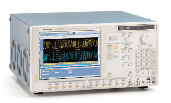
A new generation of AWGs (Figure 1), the first capable of delivering signals at the high data rates common in today's serial buses, have arrived. The new instruments offer sample rates up to 20 GS/s, with multiple outputs and ample memory to support long pattern sequences. This new development promises to transform serial measurements, particularly on the receiver side.
Why Analog?
Serial signals are made up entirely of simple ones and zeros – binary data. Why would one want to use analog waveforms to express digital data? It is because digital signals, underneath it all, are analog events. The zero rise time and the perfectly flat tops of textbook digital signals are fiction. Electronic environments have noise, jitter, crosstalk, distributed reactances, power supply variations, and other shortcomings. Each takes its toll on the signal. A real-world digital "square wave" rarely resembles its theoretical counterpart. An analog waveform source's strength is its ability to mimic analog imperfections.
Direct synthesis techniques allow engineers to create signals that embody the effects of propagation through a transmission line. Rise times, pulse shapes, delays, and aberrations all can be controlled. This is exactly what needs to be done for rigorous serial bus testing.
Intentionally-applied anomalies are not the only benefit of the direct synthesis AWG approach. The instrument can create multi-level signals containing high, low and idle states without the aid of external tools. It can produce data in any format with embedded jitter or noise, again without help from external modulators. Unlike other solutions, an AWG can originate a test signal with all the needed timing, amplitude, and distortion characteristics rather than producing a clean signal and degrading it after the fact.
Seeking the Best Solution for Worst-Case Signals
The common serial data receiver, an element used by the hundreds in digital systems of all kinds, poses one of the biggest challenges for designers who need to exercise and characterize emerging devices. The fundamental questions revolve around whether the receiver will work in the end-user application and what is the worst-case behavior.
These questions are important because signals traversing a transmission link tend to degrade in direct proportion to their clock and edge rates. Even the most carefully controlled link has more impact on, for example, a 6.0 Gb/s signal than a 500 Mb/s signal. Next-generation serial standards will see data rates escalate to 6.0 Gb/s and beyond, with no end in sight. Serial data signals are demanding more and more of the circuit elements that deliver them.
Equally important, real-world applications often stray from the ideal of a controlled-impedance signal path with minimal length and minimal disruptions. Practical manufacturing economies dictate the use of relatively lossy media such as FR-4 epoxy circuit boards. Packaging requirements rather than electrical considerations drive circuit layouts. And massproduced cables and connectors routinely trade off signal fidelity in favor of cost-effective simplicity. System designers knowingly balance transmission path integrity against the realities of cost and competition.
Consider just one effect of these choices, the impact of a lossy medium on the signals that pass through it. At high data rates the pulse amplitude decreases steadily over the length of the path, potentially reaching a level too low to guarantee accurate threshold decisions at the receiving end. In addition, effects such as edge degradation and overshoot (also shown) play a role in compromising the signal's intelligibility at the receiving input.
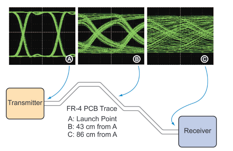
What is the cause of these losses? A high-frequency signal that propagates through a long PCB trace experiences dramatic degradation due to the loss tangent of the circuit board's dielectric material. A high loss tangent relates to high dielectric absorption, which increases attenuation at high frequencies. While Figure 2 does not denote the performance of a specific medium, its underlying message is that signals will suffer in proportion to the lossy characteristics of the medium.
Figure 2 shows what happens to a serial data signal as it passes through an FR-4 circuit board environment. At test point "A" we see an eye diagram of the transmitter output. The eye is open and robust, with full amplitude and plenty of clearance around the decision points.
At test point "B," halfway through the trip to the receiver input, the signal is already showing some wear and tear. The eye is closing and jitter is increasing, causing the edge placements to "blur." Only a very generous mask tolerance would allow this eye diagram to pass the compliance test.
At point "C," the signal is all but unintelligible. The eye opening is a tiny area somewhere near the center of the image. It would be very difficult for the receiver to respond correctly to the data transitions in this signal.
In the computing and communications industries, designers have searched for ways to improve signal transmission. Various forms of equalization, de-emphasis, and encoding have been adopted, and the gross distortions seen in Figure 2 have been tamed to some extent. But ultimately these behaviors are a result of the physics of materials, electricity, and radiation. They will always be present to a degree. For this reason, it will always be necessary to test components and systems with degraded signals – a job ideal for direct synthesis signal sources.
Direct Synthesis Approach Simplifies Receiver Jitter Tolerance Tests
Jitter is a phenomenon that can have drastic effects on circuit behavior. Data generator (DG) platforms, also known as timing/pattern generators, have long been a mainstay of serial measurements including receiver jitter tolerance tests. The following explanation will contrast the DG and pattern generator method with an emerging alternative that uses a direct synthesis toolset.
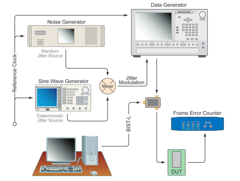
Jitter tends to "smear" edge placements and narrow the eye opening. Figure 3 depicts a typical test setup for jitter measurements on a receiver (actually a transceiver in most instances, but the receiver is the element of interest here). The figure illustrates the equipment required to deliver data patterns bearing both random and deterministic jitter. For the sake of clarity here and in subsequent illustrations, each paired differential connection to and from the DUT is shown as a single path.
This approach requires adjusting the jitter and noise content to introduce specific amounts of total jitter to the DUT until it starts sending frame or bit errors. The jitter amplitude is measured to determine whether the device meets its specifications. The goal of the equipment configuration is to stand in for real-world system components, producing any type of jitter the DUT can be expected to encounter in its end-user applications.
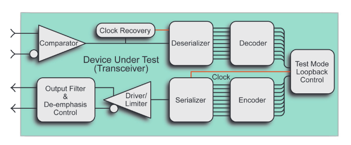
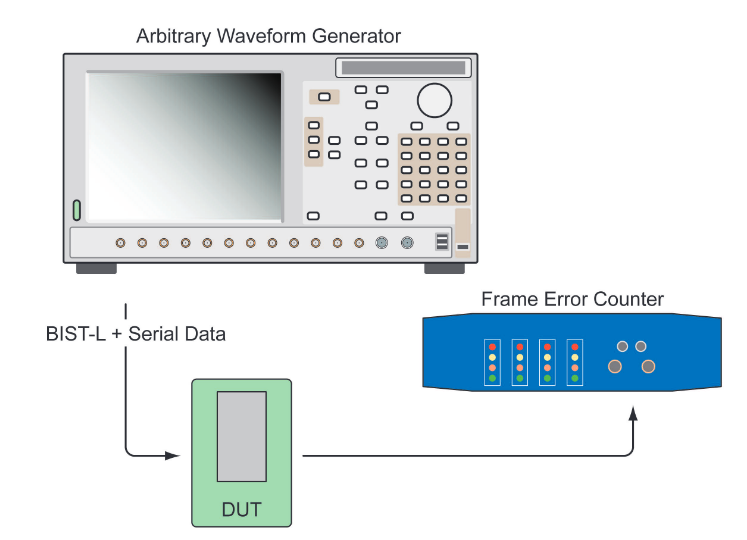
Testing a receiver for jitter tolerance is complicated by the receiver's fundamental architecture. Compliance tests such as SATA gen I and II require the DUT to follow Built-In Self Test (BIST) instructions delivered with a specific Frame Information Structure (FIS). Serial transceivers (with transmitter, receiver, and SERDES elements) are designed to go into a special loopback mode when they receive a specific sequence of BIST-L (loopback) frames. When the device is in this mode, the transmitter echoes the signal that has been received. This approach is necessary because the entire transceiver is usually implemented on one silicon chip, making the internal signal paths inaccessible. There is simply no way to probe the signals after they enter the comparator element on the receiver side of the device. A block diagram of a typical transceiver is shown in Figure 4.
Historically, BIST instructions have been provided by an external PC running an application designed for the purpose. Unfortunately, most transceivers switch out of the loopback mode and return to normal operation as soon as the BIST source is disconnected. This makes it impossible to run the tests!
The usual solution for this challenge is to feed the BIST commands to the DUT through a power combiner. The other input of the power combiner is connected to the signal generator that will provide the test data stream as shown in Figure 4. With the power combiner in the test circuit, the data generator can begin driving the test data to the DUT as soon as the loopback mode is activated, with no disconnection required.
The power combiner is a workable solution, but it is not without its tradeoffs. Clearly it adds a level of complexity and another opportunity for misconnections, poor electrical contact, and other mechanical problems. It also necessitates calibrating all of the input sources to ensure that the jitter components are introduced correctly. Most importantly, the power combiner attenuates the data signal voltage by up to 50%. Often this can be counteracted by increasing the data generator's output amplitude, but there are always limits to the instrument's performance; moreover, increasing the amplitude inevitably increases noise and potentially, distortion.
Still, the power combiner approach has been the conventional methodology for most receiver jitter testing until recently. It uses proven tools and delivers satisfactory results when the equipment and procedures are properly set up. A data generator-based setup can deliver a fixed jitter profile that meets the needs of many applications.
Another Approach to Jitter Generation
An alternative method is emerging, however. Using AWG direct synthesis techniques, it is possible to eliminate the external elements required to modify and modulate DG or pattern generator-produced signals. With a suitable direct synthesis AWG, jitter in any form can be merged into the test signal itself. The effects of both random and deterministic jitter can be modeled. The AWG's ability to vary imposed effects such as jitter in both quantitative and qualitative terms is also valuable, and easy to accomplish with software tools.
There is another significant advantage to the AWG direct synthesis approach: the instrument can incorporate the BIST-FIS instructions as part of the data. In other words, the AWG's output is one contiguous stream containing first the BIST-FIS commands and then the jittered data, with no unwanted interruptions between the two. There is no need for the power combiner or the PC running the BIST-FIS application. Figure 5 shows an AWG-based jitter measurement system made up of just two instruments: one to produce the input and one to read the output. The AWG's memory doesn't distinguish between BIST-FIS data, out-of-band signals, clock signals, or the actual data stream and its anomalies. The memory simply stores sample points that can reconstruct any waveform.
Direct Synthesis Has an Answer for De-Emphasis Measurements
Like the jitter measurements just described, there are at least two approaches for dealing with de-emphasis, a signal conditioning step designed to reduce inter-symbol interference (ISI).In this section we will again contrast the alternatives.
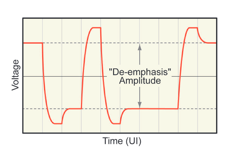
ISI can occur when a group of successive serial bits of the same state cause a buildup of energy in transmission components, with the result that pulses begin to spread in time and even overlap. Eventually the receiver has difficulty distinguishing changes of state. ISI began to plague serial bus transmission channels as bit rates accelerated into the gigabit range. Detecting and eliminating ISI has been the focus of a tremendous amount of research effort.
The accepted cure for ISI is de-emphasis. The de-emphasis technique assumes that, for any series of bits having the same binary state, the first bit (known as the transition bit) must have a greater amplitude than the bits that follow it to compensate for the frequency characteristics of the transmission line and improve signal fidelity at the receiver input. By making the transition bit higher in amplitude than the subsequent bits, the signal will arrive at the receiver pins with an "open eye." The concept is illustrated in Figure 6.
Like any other treatment that affects signal amplitude and wave shape, an emerging serial device's response to de-emphasis must be evaluated thoroughly during the design phase. Moreover, de-emphasis measurements are part of most compliance test regimes, including those for PCI Express II, Ethernet, XAUI and more.
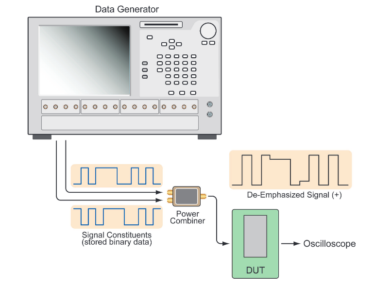
The Data Generator is the traditional solution for de-emphasis evaluation. Although the DG requires two differential output channels to deliver one signal with de-emphasis, a modern multi-output DG can be equipped with more than enough outputs to do the job. A typical DG configuration might have 8 channels – sufficient for four "lanes" of a serial bus such as PCI Express. With the growing importance of multi-lane serial architectures (the PCI Express standard encompasses variants having up to 16 lanes) as a solution for maximizing data throughput, the DG's future in de-emphasis testing is assured.
De-emphasis testing with a DG requires an external power combiner to mix two constituent data streams, offset from one another in time, and produce a single composite output – the de-emphasis signal. The test setup is shown in Figure 7. Here again, each single path in the illustration represents a differential pair. The constituent data is stored within the DG as individual binary bits that are read in each operational cycle, such that a "1" in the DG memory becomes a single "1" in the pattern.
The AWG Way to Produce De-Emphasis Signals
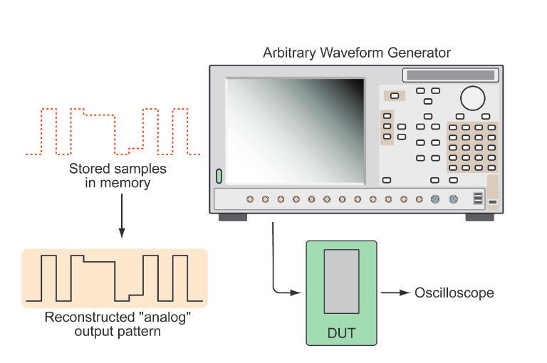
The direct synthesis method of producing the de-emphasis signal is entirely different from that of the DG, although the resulting signal applied to the DUT is identical.
The AWG's stored signal incorporates the de-emphasis. There is no need to generate and externally combine two constituent data streams to make a composite signal. As Figure 8 shows, this is a simpler arrangement than that of the DG-based configuration.
AWG Merges Spread Spectrum Clock (SSC) Into Serial Data Stream
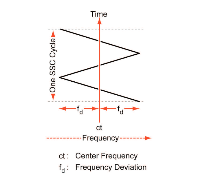
Spread-spectrum clocking is an effective way to minimize radiated EMI from clock sources in high-speed systems. Increasingly, serial standards are implementing SSC, with the result that SSC has become a compliance issue. In effect, the clock rate of the data is modulated such that the clock frequency is constantly varying. The modulation frequency is usually in the range of tens of kHz. Figure 9 illustrates the SSC concept.
While generating a compliant SSC signal can be a challenge, it is well within the capability of direct synthesis signal generation tools. Most importantly, the SSC can be embedded in the original data, just as it would be in a real serial system. The AWG output, a data stream containing SSC clock modulation, can be applied directly to the DUT with no external signal modifiers needed. This configuration can be seen in Figure 5.
Out-Of-Band Compliance Tests Need Analog Signals
Multi-level signals with at least three states – high, low and idle – are common in out-of-band (OOB) operations such as Serial ATA COMWAKE. This is an inter-device communication signal with bursts of data separated by an idle bus condition. The signaling occurs at lower frequencies than those encountered in the data path. The idle condition is essentially a tri-state level that falls between the true binary "1" and "0" values.
The idle state is exactly the sort of signal characteristic that brings out the strengths of direct synthesis. An AWG can generate discrete amplitude levels that closely approximate the idle condition, no matter what its actual voltage level might be. In doing so, it creates an OOB sequence the DUT can recognize, after which the DUT sends its own response signature. The test involves adjusting the AWG's output amplitude to determine the point at which the DUT stops responding. Once this point is established, a quick amplitude measurement with an oscilloscope can confirm the device's compliance with specifications.
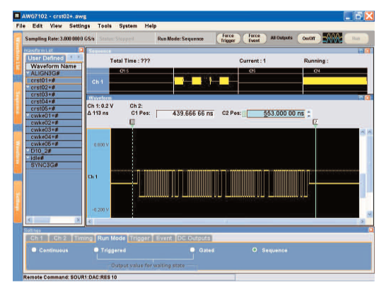
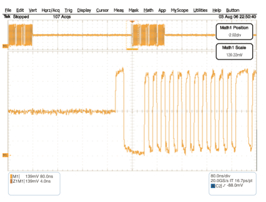
By eliminating the need for external signal modifiers such as power combiners, the AWG can create an accurate tri-state voltage value just as easily as the binary pattern values that surround it. Figure 10 is an AWG control screen showing the ComWake sequence. Figure 11 is an oscilloscope screen view showing an OOB signal that results when the AWG executes the commands on the Figure 11 screen.
Where Do Waveforms Come From?
The value of building up analog waveforms to produce digital signals cannot be overstated. The technique provides unsurpassed flexibility to design not only the basic pulse shapes, but also the modifications, imperfections and stresses that really test a new design's functionality.
Where do all these signals come from? Is it necessary to manually position every sample point?
Not at all. Today's waveform generation platforms offer a variety of methods for "authoring" signal formats. Some instruments have built-in editors; others offer sequencers that can loop, jump, and repeat segments to produce waveforms.
Some new AWG tools run on an integral PC with the Windows® operating system, enabling users to run powerful custom software applications on the instrument itself. These tools can take advantage of jitter generation, preset and custom algorithms, and other resources to create complex waveforms. The self-contained PC platform makes it easy to maintain libraries of waveforms and to network the instrument to servers housing waveform archives.
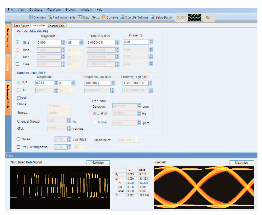
Figure 12 shows SerialXpress® custom application that runs directly on the AWG or on on an external PC. This Tektronix tool enables users to easily add jitter and channel artifacts such as random noise and deterministic jitter components to the data pattern. With SerialXpress® software it is also possible to add de-emphasis, SSC, and other effects routinely required in serial testing.
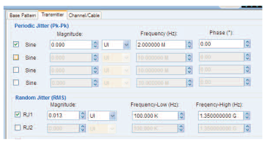
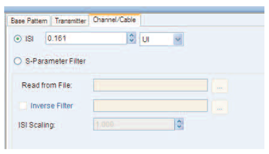
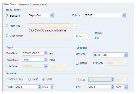
SerialXpress® software simplifies the task of designing a waveform with embedded Periodic and Random Jitter components, see Figure 13, but its capabilities do not end there. Other menu choices allow the user to enable ISI, see Figure 14, to specify the pattern type, and to define the rising and falling edge characteristics independently, see Figure 15.
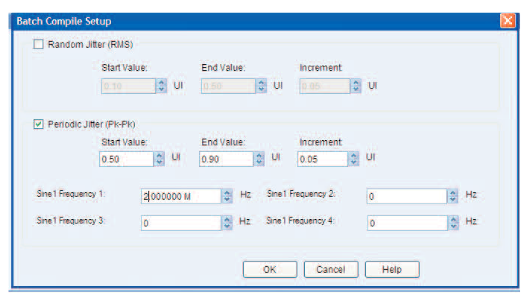
SerialXpress® also allows the user to create a series of waveforms that can be used to characterize devices through a range of specific jitter values. See Figure 16. This waveform development tool illustrates the innate flexibility of an AWG and direct synthesis generation operating within a full-featured PC environment
Working from the entered values, the application compiles and creates the AWG file that is automatically loaded into a Tektronix AWG7000 Series arbitrary waveform generator. The AWG7000 Series, due to its up to 20 Gs/s sampling rate and analog bandwidth of 5.8 GHz can accurately generate serial data streams up to 6 Gb/s using the direct synthesis approach. The 6 Gb/s is a theoretical limit derived from the maximum sample rate with adequate over-sampling to accurately recreate the required jitter for the specific compliance test. Its 64 Megasample memory depth is more than enough to support long, detailed patterns for eye diagram analysis. The AWG7000 Series AWGs can also provide up to 128M of memory when using its interleave mode.
Particularly when preparing for compliance testing, it is wise to check one's work; to acquire the AWG's output and verify its RJ, DJ, and ISI content with a high-performance oscilloscope. SerialXpress® software simplifies this calibration feature.
Capturing the Waveform
Sometimes the best way to emulate a real-world environment is simply to reproduce an actual real-world signal. SerialXpress® software also makes it possible to import acquired waveforms directly from compatible oscilloscopes or other AWGs. The AWG records a waveform that embodies exactly the amplitude, timing, and aberrations found in the source. In addition to playing back a captured signal, the software can add anomalies to the waveform for stress testing.
AWG's Digital Outputs Add Flexibility
Some AWG platforms provide up to four differential digital outputs in addition to their analog ports. These binary signals are known "markers," designed to deliver high-quality digital pulses with programmable timing and amplitude. These signal attributes are controlled independently of the AWG's main analog output. The marker outputs can be used wherever a digital signal is required but is not expected to stress the device with analog effects. In fact, these signals are so useful that many designers have purchased AWGs strictly for the marker outputs, finding them to be a cost-effective digital signal source.
The markers can be used for serial amplitude sensitivity testing and as a tool to test timing skew between serial data lanes. The marker outputs deliver data rates up to 10 Gs/s and provide testing up to 10Gb/s data rates with exceptionally low jitter. This is important because it minimizes the AWG's jitter contribution to the measurement.
Conclusion
Direct synthesis tools like SerialXpress® software are earning a place on the serial designer's bench. They have the ability to create signals with all the characteristics needed for compliance measurements, stress testing, and troubleshooting. These characteristics range from simple SSC clock modulation to complex jitter and signal distortions.
Direct synthesis platforms – arbitrary waveform generators – have only recently entered the arena of gigabit data rates. But emerging high-bandwidth (10 GS/s) AWG products are uniquely positioned to solve some long-standing problems for the serial designer. They will enable serial measurement solutions that are simpler and faster to use, while being almost infinitely flexible.