Contactez-nous
Chat en direct avec un représentant Tek. Service disponible de 9 h à 17 h, CET jours ouvrables.
Appelez-nous au
Disponible de 9 h à 17 h CET jours ouvrables.
Télécharger
Télécharger des manuels, des fiches techniques, des logiciels, etc. :
Feedback
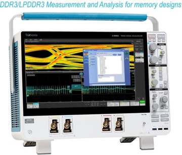
DDR3 and LPDDR3 Measurement and Analysis
6 Series MSO Option 6-CMDDR3 and Option 6-DBDDR3 Application Datasheet
Plus d’informations
- Oscilloscope à signaux mixtes MSO 64B, 66B, et 68B
- Découvrez d'autres modèles Logiciel pour oscilloscopes, produits keithley, et RF
Lire en ligne :
Key features
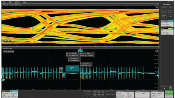
- Complete test coverage and fully automated conformance testing of DDR3 and LPDDR3 measurements as per the specification, including Eye diagram test on data and clock.
- Ability to simultaneously define Read and Write searches and perform specific DDR measurements on the qualified bursts over long record lengths.
- Ability to set voltage threshold levels per measurement as per the specification.
- Intuitive user interface and workflow to configure and perform DDR electrical validation.
- Easily switch from Conformance test environment to Debug environment on the scope to get deeper insights into test failures.
- Optionally save setup files in Conformance test suite, to be able to recall the scope state post-execution.
- Automated report generation saves measurements, test results, and waveform images in .MHT, .CSV or .PDF file format. CSV format helps to parse and customize the test reports as per your needs.
Supports a wide range of interposers for different memory standards, along with best-in-class probes, to meet signal integrity requirements.
DDR3/LPDDR3 automated testing with Opt 6-CMDDR3
Opt. 6-CMDDR3 solution lets you to perform automated DDR3 and LPDDR3 conformance testing. This solution works in conjunction with Opt. 6-DBDDR3 to add specific measurements, configure these measurements, and fetch the results post-analysis. This helps you to avoid manually saving and recalling scope setup files. The Python sequencer enables the fast execution of 100+ measurements and ensures that test validation is completed quickly.
In the DUT panel where you can choose the device type and device profile which includes the speed grade supported by the DDR device and configure the Vdd and Vref settings.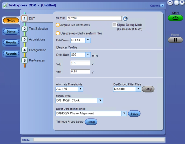
You can choose to optionally provide the filter files (.flt) relative to the hardware components used in the signal path, which will be de-embedded from the captured signal prior to analysis using the scope MATH subsystem.
DDR signal is bursty in nature and one of the first steps when it comes to DDR testing is to separate and qualify valid Read and Write bursts. The measurements are then performed on these qualified bursts.
The DUT panel provides you with a choice of several burst detection methods. Depending on the probing mechanism, you can choose the signal type settings, which help configure the signal sources accordingly during execution. By using probe mode, you can change the probe configurations.
Opt. 6-CMDDR3 supports the Signal Debug mode in the DUT panel. This mode allows you to configure the scope settings manually without the settings being overridden by the automation software. In this mode, you can provide channels, references, or MATHs as inputs to the software.
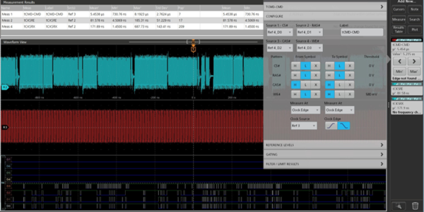
The test selection panel lists the DDR measurements as logical groups depending on the signal type selection in the DUT panel. This helps you complete the automated measurements with no manual intervention. Eye diagram tests on data and clock signals are enabled beyond the conformance requirement, so you gain deeper insight into the memory designs.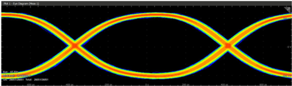
Once the execution is completed, the software generates a detailed test report with setup information, test summary, and detailed results with pass/fail status, limits, and test specific images.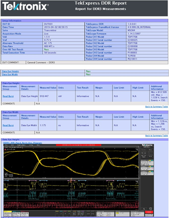
To debug test failures, Tektronix offers 6-DBDDR3 measurement package integrated into the scope measurement subsystem, which helps you to easily configure and test their memory designs.
DDR3 debug with Opt 6-DBDDR3
Opt.6-DBDDR3 lets you capture long records, automatically separate Read and Write bursts based on selected measurements, and perform measurements over multiple Read or Write bursts. You can define multiple Read and Write searches and continuously run the DDR3/LPDDR3 measurements on the qualified searches and perform statistical analysis on the results.
DDR3 electrical testing and timing analysis requires a 6 Series MSO oscilloscope with a recommended bandwidth of 8 GHz to cover entire range of DDR3 speed grades. However, for signal integrity testing and debug, a minimum bandwidth of 4 GHz would suffice most of your needs.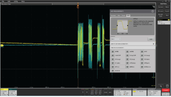
Automated read and write burst detection
Some JEDEC conformance measurements require isolating the events of interest such as read or write bursts on the memory bus, which is automatically handed by the Conformance solution.
For debug, it may be necessary to further isolate certain events by a particular rank or bank, or to isolate certain data patterns for analysis of signal-integrity issues such as data-dependent jitter, timing, or noise problems. The simplest way to achieve this is to use the DQS (Data Strobe signal) to identify the start of a read or write burst. For example, DDR3 always asserts DQS high at the start of a write, or low at the start of a read.
The Visual Trigger feature on the 6 Series MSO oscilloscope lets you further condition traditional triggers for more versatile DQS burst capture capability. Visual Trigger lets you create mask-like areas directly on the waveform display, where the boundaries of the areas help define trigger events for a DQS or Data Strobe signal.
Making the complex easier
The JEDEC specifications for each memory technology specifies an array of conformance measurements. These measurements include clock jitter, setup and hold timing, transition voltages, signal overshoot and undershoot, slew rate and other electrical-quality tests. These tests are complex to measure using general-purpose tools.
Because the JEDEC-specified measurement methods require reference levels, pass/fail limits, and more, it is extremely valuable to have an application-specific measurement utility for DDR testing. Opt. 6-CMDDR3 is designed to correctly set up DDR measurements for specified devices. The broad set of measurements available in 6-CMDDR3 conforms to the JEDEC specifications. You can also leverage Opt. 6-DBDDR3 to customize settings to measure non-standard devices or system implementations.
Option 6-CMDDR3 works with option 6-DJA (Advanced Jitter Analysis) to provide Jitter and Eye Diagram Analysis Tools. These two utilities work together to create a powerful, flexible, and easy-to-use test suite for DDR testing and debug.
DDR search feature
The DDR search feature lets you search an entire waveform acquisition for specific signal conditions, such as DDR Read/Write, and mark the waveform where the conditions are met. In addition to using these marks for visual analysis, the oscilloscope can apply the marks as qualifiers for DDR-specific measurements, so that the measurements occur only on the appropriate portion of the data stream. The search algorithms in DDR search make use of the fact that DDR phase relationships are different for read and write bursts; DQ and DQS are in-phase for reads, and 90 degrees out-of-phase for writes. It also supports burst identification based on Chip Select (CS) signal and digital signals (Chip Select-CS, Row Access Strobe-RAS, Column Access Strobe-CAS, and Write Enable source-WE).
Steps to debug failures
The first step in memory debugging is to define a search. This can be done by clicking on the Search button on the scope and defining a DDR search on Read or Write bursts. The next step is to add the measurement from DDR tab and configure these measurements. The configuration involves providing search as an input to the measurement and defining signal sources. Since there are multitude of measurements to be configured, it is recommended to configure the measurements manually one time and save the scope setup file. When you want to debug next time, it is easy to recall the scope setup file, which brings back all the configured measurements on the scope and make edits as necessary.
Once the setup is complete and you select <Run> (or <Single>), the oscilloscope acquires the signals of interest, identifies and marks qualified data bursts, and updates the results for the selected measurements.
The factory setup files supplied with 6-DBDDR3 package are built with industry-standard measurement settings, you may need to modify the settings one time and save them if your test setup is different than the default setup files.
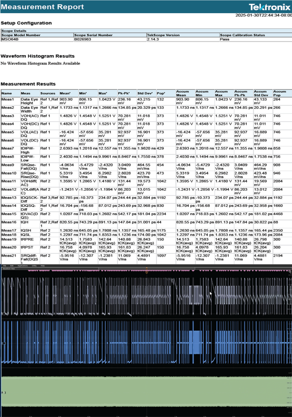
You can view results in table format by clicking on Results Table button on the scope screen. The results table displays all measurement results with their statistical population, sources and other relevant data. You can generate a report, with an option to save the waveform data that is used to make these measurements.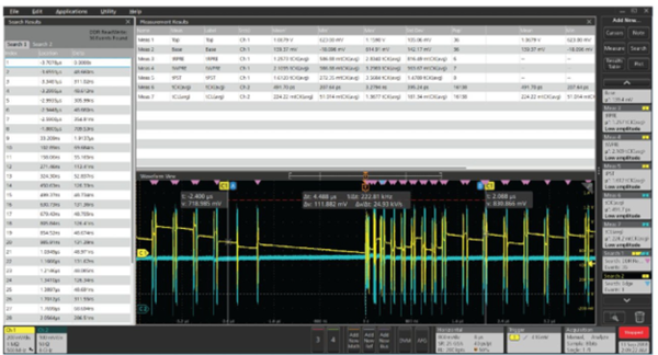
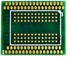
DDR3 Main memory interposers
Gaining access to signal test points on a memory chip is a significant challenge in DDR testing. The JEDEC standards requires that measurements should be taken at the Ball Grid Array (BGA) ballouts of the memory component, connections that are very difficult to access.
Tektronix, in partnership with Nexus Technology 1, offers probing options such as BGA interposers that supports different memory devices in a variety of form factors. The interposer includes an embedded tip resistor placed close to the BGA pad. The DDR3 main memory is available in standard BGA component packages as well as dual-inline-memorymodules of DIMM and SODIMM.
Standard BGA packages are soldered directly to the Printed Circuit Board (PCB) while modules comprise a series of packages in a standard PCB format with standard connections between the DIMM and the main board. Interposers are available for both component packages and DIMM and SODIMM modules.
Introduction of an interposer and an oscilloscope probe may change the characteristics of the signal. Apply de-embedding filters to remove the effect of the interposer and a probe in the signal path to get an accurate representation of the signal at the probe point.
EdgeProbe interposer
The Nexus Technology patented EdgeProbe™ interposer is available for DDR3, LPDDR3, and other new memory products. It has a small mechanical footprint as the probe points are on the edge of the interposer. The probes can attach directly to the target device to provide access to the clock, command bus, data, strobe, and address signals.
The EdgeProbe design removes mechanical clearance issues as the interposers are the size of the memory components. Embedded resistors within the interposers place the oscilloscope probe tip resistor extremely close to the BGA pad, by providing an integrated oscilloscope probe on all the signals.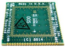
Socketed interposer
A socketed interposer typically provides access to all component signals and elevates the interposer above adjacent components for mechanical clearance. This solution offers a custom socket that is installed on the target and has an interposer that is installed by pressing it into the socket. Retention is designed into the solution since the interposer can be removed by pulling an unsecured interposer from the target socket.
The interposer can have the memory component soldered directly to it or optionally have a socket on the interposer. The socket on the interposer allows for memory components to be manually inserted and removed to easily evaluate different vendor memory components. When testing is completed, the interposer can be removed and the memory device inserted directly into the custom socket on the target, removing the effect of the interposer.
Direct attach interposer
The direct attach interposer enables probing of all signals and is installed directly onto the target. The target must have mechanical clearance for the interposer. The use of the direct attach interposers is common for Package on Package (PoP) components.
| Technology | Package / Form factor |
|---|---|
| DDR3 | Socketed – 78 Ball / 96 Ball Edge Probe – 78 Ball / 96 Ball Solder-down – 78 Ball / 96 Ball DIMM and SODIMM Interposer for MSO |
| LPDDR3 | Socketed – 216 Ball / 211 Ball Solder-down – 178 Ball / 211 Ball |
TDP7700 series TriMode probes for DDR3 measurements
The Tektronix TDP7700 Series TriMode probes are designed to meet DDR3 measurement challenges. The TDP7700 works with the 6 Series MSO, with full AC calibration of the probe and tip signal path, to provide the highest probe fidelity available for real-time oscilloscopes. The innovative new probe design uses SiGe technology to provide the bandwidth and fidelity needed today and in the future.
TriMode probing lets one probe setup take differential, single ended, and common mode measurements accurately, increasing your efficiency. This unique capability lets you switch between differential, single ended and common mode measurements on the oscilloscope without moving the probe connection point.
A key TDP7700 connectivity innovation is using solder-down probe tips with the probe input buffer mounted only a few millimeters from the tip. This approach provides unmatched usability for connecting to DDR3 circuits.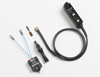
Other TDP7700 Series probe characteristics include:
- Excellent step response and low insertion loss up to 20 GHz
- Low-DUT loading with 100 kΩ (DC) and 0.4 pF (AC) performance
- High Common-Mode Rejection Ratio (CMRR)
- Low noise
TLP058 FlexChannel® logic probe for digital measurements
The 6 Series MSO provides digital channel capabilities to perform full protocol analysis of the entire memory bus. The TLP058 FlexChannel® logic probe connects the Tektronix 6 Series MSO to digital buses and signals on the device under test (DUT). The probe contains eight data channels and connects the TLP058 logic probe to any FlexChannel oscilloscope input channel.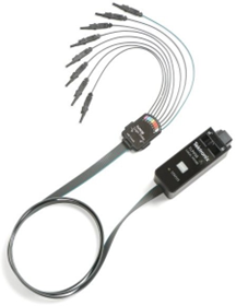
Specification
Timing measurements
- tRPRE measures the width of the Read burst preamble. This is measured from the exit of tristate to the first driving edge of the differential strobe.
- tWPRE measures the width of the Write burst preamble. It is measured from the exit of tristate to the first driving edge of the differential strobe.
- tPST measures the width of Read or Write burst postamble. It is measured from the last falling edge crossing the mid reference level to the start of an undriven state(as measured by a rising trend per JEDEC specification).
- Hold Diff measures the elapsed time between the designated edge of the single-ended waveform and the designated edge of a differential waveform. The measurement uses the closest single-ended waveform edge to the differential waveform edge that falls within the range limits.
- Setup Diff measures the elapsed time between the designated edge of a single-ended waveform and when the differential waveform crosses its own voltage reference level. The measurement uses the closest single-ended waveform edge to the differential waveform edge that falls within the range limits.
- tCH(avg) measures the average high pulse width calculated across a sliding 200 cycle window of consecutive high pulses.
- tCK(avg) measures the average clock period across a sliding 200-cycle window.
- tCL(avg) measures the average low pulse width calculated across a sliding 200 cycle window of consecutive low pulses.
- tCH(abs) measures the high pulse width of the differential clock signal. It is the amount of time the waveform remains above the mid reference voltage level.
- tCL(abs) measures the low pulse width of the differential clock signal. It is the amount of time the waveform remains below the mid reference voltage level.
- tJIT(duty) measures the largest elapsed time between tCH and tCH(avg) or tCL and tCL(avg) for a 200-cycle window.
- tJIT(per) measures the largest elapsed time between tCK and tCK(avg) for a 200-cycle sliding window.
- tJIT(cc) measures the absolute difference in clock period between two consecutive clock cycles.
- tERR(n) measures the cumulative error across multiple consecutive cycles from tCK(avg). It measures the time difference between the sum of clock period for a 200-cycle window to n times tCK(avg).
- tERR(m-n) measures the cumulative error across multiple consecutive cycles from tCK(avg). It measures the time difference between the sum of clock periods for a 200-cycle window to n times tCK(avg).
- tDQSCK measures the strobe output access time from differential clock. It is measured between the rising edge of clock before or after the differential strobe Read preamble time. The edge locations are determined by the mid-reference voltage levels.
- tCMD-CMD measures the elapsed time between two logic states.
- tCKSRE measures the valid clock cycles required after Self Refresh Entry (SRE) command. Changing the input clock frequency or the supply voltage is permissible only after tCKSRE time when the SRE command is registered.
- tCKSRX measures the valid clock cycles required before the Self Refresh Exit (SRX) command. Changing the input clock frequency or the supply voltage is permissible provided the new clock frequency or supply voltage is stable for the tCKSRX time prior to SRX command.
Amplitude measurements
- AOS measures the total area of the signal above the specified reference level.
- AUS measures the total area of the signal below the specified reference level.
- Vix(ac) measures the differential input cross-point voltage measured from the actual crossover voltage and its complement signal to a designated reference voltage. This is measured on a single-ended signal.
- AOS Per tCK measures the total area of the signal that crosses the specified reference level calculated over consecutive periods. It is applicable to clock and address/command waveforms only.
- AUS Per tCK measures the total area of the signal that crosses the specified reference level calculated over consecutive periods. It is applicable to clock and address/command waveforms only.
- AOS Per UI measures the total area of the signal that crosses the specified reference level calculated over consecutive unit intervals. It is applicable to data and data strobe waveforms only.
- AUS Per UI measures the total area of the signal that crosses the specified reference level calculated over consecutive unit intervals. It is applicable to data and data strobe waveforms only.
| Details | DDR3 | LPDDR3 |
|---|---|---|
| Speed (MT/s) | 800, 1066, 1333, 1600, 1866, and 2133 | 333, 800, 1066, 1200, 1333, 1466, 1600, 1866, and 2133 |
| Max slew rate | 10 V/ns | 8 V/ns |
| Typical V swing | 1 V | 0.6 V |
| 20-80 risetime | 60 ps | 45 ps |
| Report HTML | and PDF format | |
| Source | support Live analog signals, reference waveforms, and math waveforms. | |
| De-embedding | support Filter file using math subsystem. | |
Ordering information
Required hardware
| Oscilloscope | 6/6B Series MSO oscilloscope with minimum bandwidth of 4 GHz (6-BW-4000) for debug and a recommended bandwidth of 8 GHz (6-BW-8000) for DDR3/LPDDR3 automated conformance testing. |
| Operating system | 6-WIN (removable SSD with Microsoft Windows 10 operating system).Optional - Required only for DDR3/LPDDR3 automated conformance testing |
Required software
| Application | Options | License type |
|---|---|---|
| DDR3 and LPDDR3 Automated Compliance Solution for 6/6B Series MSO 2 | 6-CMDDR3 | New instrument license |
| SUP6-CMDDR3 | Upgrade license | |
| SUP6-CMDDR3-FL | Floating license 3 | |
| DDR3 and LPDDR3 Analysis and Debug Solution for 6/6B Series MSO 4 | 6-DBDDR3 | New instrument license |
| SUP6-DBDDR3 | Upgrade | |
| SUP6-DBDDR3-FL | Floating license3 |
Recommended probes and accessories
| Accessory type | Quantity |
|---|---|
| TDP7708 Tri-mode probe with P77STFLXB adapters | Two probes are required for testing a DUT with DQ and DQS. Three probes are required for testing a DUT with DQ, DQS, and clock. |
| TLP058 | One probe is required for probing CS, RAS, CAS, and WE lines. |
| TDP3500 | One probe is required for CS as Analog signal. |
| Accessory type | Vendor |
|---|---|
| DDR3: x4, x8, 16 socketed, solder-down and direct attach interposers | Sold through Tektronix and Nexus Technologies4 |
| LPDDR3: BGA and PoP interposers |
1 For a detailed list of interposers, visit nexustechnology.com
2 DDR3 and LPDDR3 Automated Compliance Solution for 6/6B Series MSO requires 6-DBDDR3 and 6-DJA as a pre-requisite for running DDR and Eye diagram measurements.
3 Floating licenses are transferrable from any 6 Series MSO to any other 6 Series MSO, for use of one instrument at a time.
4 Contact your local Tektronix representative for details.

Tektronix is ISO 14001:2015 and ISO 9001:2015 certified by DEKRA. Product(s) complies with IEEE Standard 488.1-1987, RS-232-C, and with Tektronix Standard Codes and Formats. Bluetooth is a registered trademark of Bluetooth SIG, Inc. LTE is a trademark of ETSI. 55W-61470-3


