Contactez-nous
Chat en direct avec un représentant Tek. Service disponible de 9 h à 17 h, CET jours ouvrables.
Appelez-nous au
Disponible de 9 h à 17 h CET jours ouvrables.
Télécharger
Télécharger des manuels, des fiches techniques, des logiciels, etc. :
Feedback
Simple, Expert, Rapide.
Tektronix complète votre équipe en assurant des solutions de service d'étalonnage qui permettent de gagner du temps, faire des économies et garantir la précision des équipements électroniques de test et de mesure. Nous travaillons en concertation avec vous pour vous aider à prendre les meilleures décisions d'augmentation ou d'externalisation des équipements complexes de test et de mesure. Tous les jours, des milliers d'entreprises font confiance à Tektronix pour réaliser un étalonnage de qualité OEM à un prix compétitif.
- Service couvrant les équipements de marque Tektronix, Keithley, Fluke, Keysight, Rohde & Schwartz, Agilent et plus de 9 000 autres marques d'équipements de test et de mesure
- Programme personnalisé : sur site, centre local, expédition en usine
- Temps de traitement rapide et fiable
- Gamme complète d'étalonnages accrédités Z540 et ISO 17025
- Techniciens certifiés A2LA
Lean Manufacturing
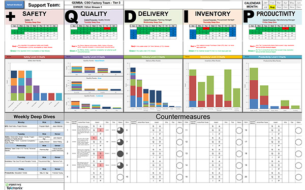
Tektronix Component Solutions applies lean manufacturing principles throughout our facility and is focused on continuous improvement to remove waste, streamline processes and ensure that assembly activities are providing value to our customers. To support this goal, our manufacturing lean cells are constantly evaluated on strict standards of safety, quality, delivery, inventory and productivity (+QDIP). +QDIP metrics are clearly communicated at each cell by a visual management system, allowing managers and operators to quickly assess performance at any given time. With these metrics as a guide, our manufacturing team consistently seeks to pro-actively enhance the design and flow of lean cells to improve performance (e.g. takt time, yield, throughput). This focus on continuous improvement helps to proactively reduce risk and ensure quality and consistent delivery.
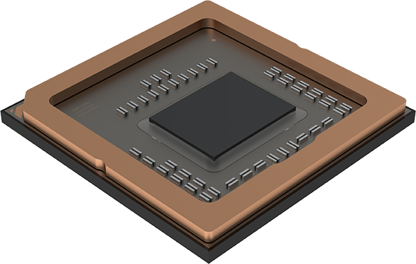
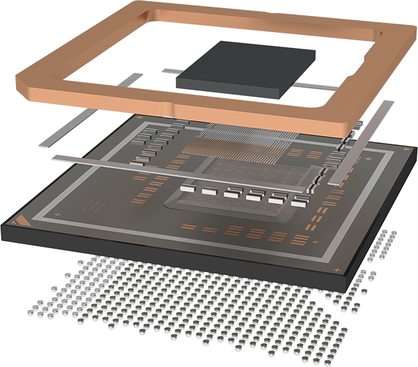
As a proven US-based, ITAR-registered supplier to a variety of defense programs and companies, Tektronix Component Solutions is an ideal partner for defense applications requiring high-performance, mission-critical microelectronics. Offering services and products that include wafer test, IC packaging assembly and test, 2.5/3D packaging, and design & simulation, Tektronix Component Solutions has the expertise and capabilities to meet your requirements for high-reliability microelectronics.
With more than 40 years of experience, Tektronix Component Solutions is the stable supplier that you can trust to deliver on long-term military programs.
Trusted, ITAR-Registered Supplier
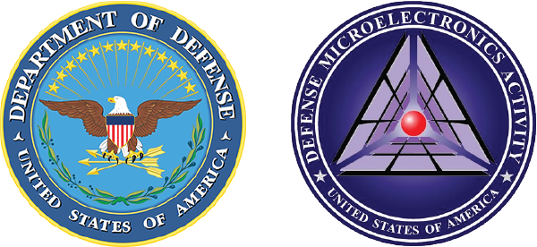
Tektronix Component Solutions has been accredited by the U.S. Department of Defense (DOD), Defense Microelectronics Agency (DMEA) as a Category 1A microelectronics Trusted Source for IC packaging/assembly and test services – the highest designation awarded by the U.S. Department of Defense. This enables Tektronix Component Solutions to serve U.S. defense customers with classified program requirements. The accreditation certifies that Tektronix Component Solutions meets stringent product control and security standards in providing trusted microelectronic services. Tektronix Component Solutions also holds certifications in ISO9001/ISO14001 and AS9100D and meets all ITAR requirements.
As an on-shore, ITAR-registered supplier, Tektronix Component Solutions has stringent standards in-place to protect and control sensitive information related to defense programs. With many years of experience supporting defense customers and programs, we recognize and adhere to the added level of responsibility in providing microelectronic engineering and manufacturing services to the military.
High-Performance Products and Services
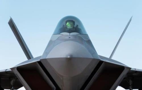
Our military experience spans a variety of critical applications, including communications, avionics, radar, propulsion control, and guidance systems. Tektronix Component Solutions has supplied high-performance and high-reliability products to defense programs such as the F-22 Raptor and F-35 Lightning II (Joint Strike Fighter) with a focus on continual C-SWaP (cost, size, weight and power) improvements.
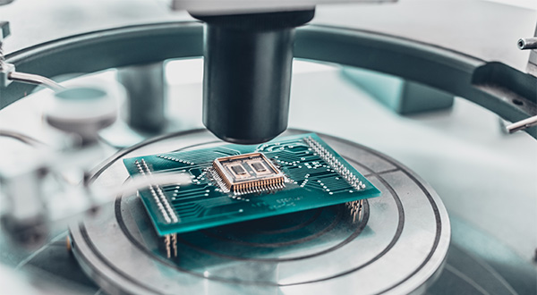
Having served military and commercial aerospace customers for many years, Tektronix Component Solutions has a deep understanding of the high-reliability requirements of those applications. As such, we fully utilize our unique strength in test to deliver fully-tested parts that have proven to operate successfully in mission-critical environments.